Low-Temperature Deposition of Transparent Conducting Films Applied to Flexible Electrochromic Devices

1
Department of Materials Science and Engineering, National Cheng Kung University, Tainan 70101, Taiwan
2
Division of Physics, Institute of Nuclear Energy Research, Taoyuan City 32546, Taiwan
*
Author to whom correspondence should be addressed.
Materials 2021, 14(17), 4959; https://doi.org/10.3390/ma14174959
Submission received: 19 July 2021
/
Revised: 23 August 2021
/
Accepted: 23 August 2021
/
Published: 31 August 2021
(This article belongs to the Section Thin Films and Interfaces)
Abstract
:Here, we compare two different transparent conducting oxides (TCOs), namely indium tin oxide (ITO) and indium zinc tin oxide (IZTO), fabricated as transparent conducting films using processes that require different temperatures. ITO and IZTO films were prepared at 230 °C and at room temperature, respectively, on glass and polyethylene terephthalate (PET) substrates using reactive magnetron sputtering. Electrochromic WO3 films deposited on ITO-based and IZTO-based ECDs using vacuum cathodic arc plasma (CAP) were investigated. IZTO-based ECDs have higher optical transmittance modulation, ΔT = 63% [from Tbleaching (90.01%) to Tcoloration (28.51%)], than ITO-based ECDs, ΔT = 59%. ECDs consisted of a working electrochromic electrode (WO3/IZTO/PET) and a counter-electrode (Pt mesh) in a 0.2 M LiClO4/perchlorate (LiClO4/PC) liquid electrolyte solution with an active area of 3 cm × 4 cm a calculated bleaching time tc of 21.01 s and a coloration time tb of 4.7 s with varying potential from −1.3 V (coloration potential, Vc) to 0.3 V (bleaching potential, Vb).
1. Introduction
The optical properties (transmittance, reflectance, and absorption) of electrochromic devices (ECDs) can be changed using a dc pulsed voltage [1]. Electrochromism is associated with double injection/extraction of positive ions (lithium or proton) and electrons into/out of electrochromic materials [2]. A wide variety of electrochromic materials have been developed, including metal oxides [3,4,5], small organic molecules [6], and conductive polymer thin films [7,8,9]. In recent years, electrochromic devices (ECDs) have attracted tremendous attention due to their potential applications, such as in smart windows [10,11], optical displays [12] and rear-view mirrors [13]. Smart windows based on electrochromic (EC) materials allow easy control of indoor sunlight and solar heat and can be used to effectively reduce the heating or cooling loads of building interiors [2,14]. Flexible electrochromic devices (FECDs) have become an important demand, and hold new possibilities for the application of ECDs, for example, for thermal control of satellites [15], potentially flexible hidden message displays and wearable smart clothes applications [16,17].
In addition, FECDs are very thin and lightweight, which makes their use more flexible than rigid ECDs. The conventional application of FECDs is seriously restricted by fabrication techniques and electrochromic materials such as flexible transparent conductive films and electrochromic (EC) materials with the desired photoelectrical properties and durability [15,17,18], which is a key point developed in FECDs. Traditional deposition techniques used to fabricate FECDs include magnetron sputtering, plasma-enhanced chemical vapor deposition, electrodeposition and lithography. The advantages of FECDs include the potential to reduce production costs using roll-to-roll deposition [19]. In general, FECDs are composed of anodic and cathodic coloring materials in a five-layer structure [20]. A pair of transparent conducting layers sandwich an ionic conduction layer (electrolyte) in contact with an electrochromic (EC) layer and an ion storage (complementary) layer—TCO/EC/IC/CE/TCO, where TCO, IC and CE are the transparent conducting oxide, the ion conducting layer (electrolyte) and the counter electrode, respectively [20,21]. Tungsten oxide (WO3) is known as one of the most popular cathodic coloration materials and nickel oxide (NiO) is a typical anodic coloration material that has been intensively investigated. A popular TCO is indium tin oxide (ITO)—the most widely used material as a transparent conducting film for electrochromic devices. However, ITO films exhibit excellent characteristics only in crystalline forms, and have to be deposited at high temperatures at least above 200 °C to be crystallized [22]. Further, its brittleness and high-temperature processing requirements limit its use in flexible devices [23,24]. Low-temperature deposition of amorphous TCOs (α-TCOs) typically occurs via overlaps of empty isotropic ns orbitals of their heavy metal cations in the electronic configuration (n − 1)d10ns0 (n ≥ 4) [25], with excellent characteristics that are comparable with that of crystalline TCOs, and thus this is a promising a new trend in optoelectronic devices. α-TCOs have been found to possess good electrical conductivity, high transmittance, high mobility [26,27,28], high thermal/chemical stability, low deposition temperatures and lower roughness. In recent years, IZTOs film have received much attention as new candidates for transparent conducting films. In this study, we compare ITO and IZTO films as transparent electrodes in ECDs using different deposition processing temperatures. FECD performance was studied as a function of the grain size of the WO3 particles deposited on the two different TCO electrodes. We applied ITO and IZTO films to FECDs consisting of a working electrode (WO3 electrode film deposited on ITO/glass and IZTO/PET) and a counter electrode (Pt mesh) in a 0.2 M LiClO4/perchlorate (LiClO4/PC) solution.
2. Experimental Methods
2.1. Methods
The typical structure of Pt mesh/electrolyte layer/EC layer/TCO substrates for coloration state indicates the movement of an injection of positive ions (lithium) and electrons into electrochromic materials as shown in Figure 1. The PET and glass substrates used were thoroughly cleaned beforehand through an ultrasonic bath sequence in acetone, ethanol, and deionized water for 15 min each and were then subsequently dried using high-purity N2 gas and loaded into the sputter chamber and the distance between the target and substrate was set at approximately 90 mm. The deposition chamber is then evacuated to a high-vacuum base pressure set to less than 9.33 × 10⁻⁴ Pa. The working pressure, set at 0.13 Pa, was kept with an argon (Ar) gas flow of 30 sccm. IZTO films were fabricated without substrate heating, while ITO films were fabricated with the substrate heated to 230 °C in the deposition process, and the target was pre-sputtered for 3 min. The individual ITO (90 at.% In2O3 + 10 at.% SnO2) and IZTO (70 at.% In2O3 + 10 at.% SnO2 + 20 at.% ZnO) films were then deposited on the substrates using DC magnetron sputtering of 100 W to achieve a final thickness of approximately 800 nm. The deposition process of TCO films is listed in Table 1. On the finished TCO/glass substrate samples, a WO3 electrode film (220 nm) layer was deposited using cathodic arc plasma (CAP) deposition with a high-purity tungsten (W)-metal target (76 mm in diameter and 12 mm in thickness) at room temperature. The base chamber pressure was set at than 1.33 × 10⁻³ Pa using a turbo pump. In this study, we used an oxygen mass flow of 375 sccm and an argon mass flow of 75 sccm for the reactive gases. The WO3 films were fabricated on individual TCOs/glass as electrochromic layers, which are listed in Table 2.
2.2. Characterization
The crystal structural properties of the TCO films were analyzed by Grazing Incidence X-ray diffraction (GI-XRD). The electrical properties of TCO films were characterized using a Hall effect measurement system at room temperature. We used a UV–vis spectrometer (USB 4000, Ocean Optics, Inc., 830 Douglas Ave. Dunedin, FL, USA) to measure the optical properties of TCO films in the wavelength range of 200–2000 nm. Using Scanning Electron Microscopy (SEM), we observed the surface morphologies of WO3 nanoparticles on the different TCO thin films (WO3/TCO/PET and WO3/TCO/glass). Electrochemical characterization was carried out using chronoamperometry (CA) and electrochemical impedance spectroscopy (EIS) (Autolab, model PGSTAT 30) of WO3/TCO/PET or WO3/TCO/glass, which were systematically discussed. In the electrolyte system, we used a liquid electrolyte composed of lithium perchlorate (LiClO4, Mw = 106.39, Sigma-Aldrich, Darmstadt, Germany) and propylene carbonate (PC, C4H6O3, Sigma-Aldrich), and the resulting weight ratio was 0.053 (LiClO4/PC = 10.6 g/200 mL). An active area of 2 × 3 cm2 was used in our case for ECDs. The Alpha-Step D-500 stylus profiler is measured with each layer of thickness. In situ optical transmittance was carried out with a U–vis spectrometer. Electrochemical impedance spectroscopy (EIS) of all ECDs was measured with the frequency range set from 1 mHz to 1 MHz.
3. Results and Discussion
Figure 2 displays the GI-XRD patterns of ITO/glass and IZTO/PET using DC magnetron sputtering power at 100 W. The GI-XRD patterns of ITO film deposited on glass at 230 °C which exhibited polycrystalline indexed at (211), (222), (400), (440), and (622). The high-intensity peak at 2θ of 35° indicates the crystalline nature of film with (222) as the preferred plane orientation. The GI-XRD patterns of ITZO film deposited on PET substrates at room temperature and exhibited a lone, broad peak at 2θ of 33°, indicating an amorphous structure.
Figure 3 exhibits the optical transmittance of ITO/glass and IZTO/PET in the wavelength range of 300–2000 nm measured with UV–vis spectrometry. The samples of ITO/glass and IZTO/PET were measured with average transmittance, sheet resistance (Ω/□), electrical resistivity(ρ), mobility (μ), carrier concentration (n) and figure of merit (ΦTC). The average transmittance of ITO/glass and IZTO/PET was calculated to be approximately 86.8% and 88.4% in the wavelength range of 400–800 nm. The mobility of IZTO was higher than ITO due to poor electron–phonon scattering because of the amorphous structures. The carrier concentration of IZTO film was lower than the ITO film due to carrier compensation. According to Haacke’s relation, in order to qualify the performance of TCO [24], figure-of-merit ΦTC can be explored by Equation (1):
where the T(λ) is the optical transmittance, Rs is the sheet resistance, and ΦTC is displayed in Table 3; the higher value of ΦTC is 40 × 10−3 for the ITO thin films fabricated with substrate heating of 230 °C than 31.1 × 10⁻³ for the IZTO films fabricated at room temperature.
ΦTC = T(λ)10/Rs,
Figure 4 shows the SEM images of WO3 films deposited on ITO/glass and IZTO/PET. From SEM images, we find that the WO3 particle of the IZTO-based ECD is smaller than the ITO-based ECD. Patrick et al. [29] suggested that the rough surface raises the local supersaturation in the solution, thus leading to another mechanism of enhanced nucleation rate. The IZTO film was featureless and smooth without defects such as pinholes, cracks, and protrusion [30] that could control the WO3 particle size in furthering the process.
We sought to elucidate the electrochemical properties of the WO3/ITO/glass and WO3/IZTO/PET by constructing three electrode cells, which comprised a working electrode (WO3 film on TCO substrate), a counter-electrode (Pt mesh) and a reference electrode (Ag/AgCl) in a 0.2 M LiClO4/PC solution [31,32].
Figure 5 displays the CA curves at a voltage of 0.3 V (bleaching state) to −1.3 V (coloring coloration state) with a pulsed time interval of 30 s for the coloration and bleaching states of the optical transmittance spectra of WO3/ITO/glass and WO3/IZTO/PET in the range from 300 to 1000 nm. Optical transmittance modulation (∆T = Tbleaching − Tcoloration) of IZTO-based ECD and ITO-based ECD varied at 63% and 59%. The transmittance optical modulation, ∆T = 63% between coloration and bleaching states, with IZTO-based ECDs higher than ITO-based ECDs at a fixed wavelength of 633 nm due to relevant surface electrochromic materials (WO3/ITO/glass and WO3/IZTO/PET) for particle size discussed in detail below.
FECDs involved the double injection/extraction of positive ions (lithium or proton) and electrons into/out of the host WO3 lattice in the transition from W5+ to W6+. This follows the electrochemical reaction:
during applying the negative voltage, the reduction of W ions W6+ to W5+ led to the coloration state, and the reverse voltage the oxidation of W5+ to W6+ to the bleaching state.
WO3 (bleaching state) + x (Li+ + e−) → LixWO3 (coloration state),
To clarify the outstanding optical transmittance difference of IZTO-based ECD and ITO-based ECD, the behaviors of Li+ ions and electrons in the transport process were considered. Figure 6 shows the bleaching state for electron and Li+ ions extraction transport in electrochromic WO3 films when applying the positive voltage. Li+ ions and electrons can extract a distance of d out LixWO3 (where d represents the maximum electron and Li+ ions from the interior of LixWO3, R1 and R2 represent the radius of LixWO3 particle for ITO-based and IZTO-based ECDs, respectively.) It presumes R2 (the radius of LixWO3 particle for IZTO-based ECDs) is smaller than d (the distance of Li+ ions and electrons can extract), which can explain electron and Li+ ions can be extracted from the interior of LixWO3 for IZTO-based ECDs. However, R1 (the radius of LixWO3 particle for ITO-based ECDs) is larger than d (the distance of Li+ ions and electrons can extract), and this means electron and Li+ ions cannot be extracted to the electrolyte from the LixWO3 particle completely, indicating the LixWO3 particles have some residual W5+ ions in the process of fading oxidation that W5+ cannot completely convert to W6+, leading to poor optical transmittance modulation [31,32].
Figure 7 shows CA curves with varying potential from −1.3 V to 0.3 V for 30 s and the corresponding in situ transmittance response of IZTO-based ECD and ITO-based ECD at a fixed wavelength of 633 nm. Furthermore, the switching response times of the coloration and bleaching states are defined as reaching 90% of the full transmittance modulation investigated in detail in Table 4 [33]. In this study, IZTO-based ECD and ITO-based ECDs were calculated as a tc of 21.01 s and 20.13 s, and as tb of 4.7 s and 22.32 s, respectively. In general, the bleached response time presented faster coloration kinetics than coloration due to the lower conductivities of the bleached-state forms than those of the colored-state forms [33]. The bleaching time is determined by the dispersion coefficient of ions and the length of dispersing channels [34,35]. The fast bleaching time of IZTO-based ECDs is associated with the WO3 particle size due to the shorter dispersing channels.
Figure 8 shows a schematic of the electrochemical reaction for the Pt mesh/electrolyte layer/EC layer/TCO substrate at the coloration state, which can be expressed as the sum of the following [36]
R = Rs (electrolyte) + Rct (LixWO3) + R (WO3) + R (TCO/WO3) + R (TCO)
The ions for the intercalation process are supplied using an Electro-Chemical Impedance spectroscopy (EIS) tool to analyze the ion charge transfer properties of IZTO-based and ITO-based ECDs. Further, we compare the charge transport kinetics of the two TCO electrodes based on ECDs via a Nyquist curve analysis.
Figure 9 shows that there are three processes involved in the intercalation of ions into electrochromic WO3 films. First, the left point of the semi-circle, in the high-frequency region, indicates the migration of ions at the electrode–electrolyte interface. Secondly, the middle of the semicircle, in the middle-frequency region, corresponds to the charge-transfer process. Third, the right part of the semi-circle, in the low-frequency region, indicates the migration of ions at the electrode–electrolyte interface. Electrolyte solution resistance Rs was found in the high-frequency region in intercept of the semi-circle real impedance axis on the Nyquist curve [37]. The Rs value of IZTO-based ECD was approximately 4.9 Ω, which is similar to the ITO-based ECD (4.5 Ω). The semicircle in the middle frequency region can be ascribed to the charge-transfer interphase resistance Rct of the Li+ ions dependent on the diameter of the semicircle across the interphase electrolyte and WO3 films. The results show that the ITO-based ECD reveals a larger semi-circle with approximately 9.5 Ω resistance that was smaller than the IZTO-based ECD of 13.5 Ω, and is demonstrating a smaller charge carrier interphase resistance. The inclined line indicates the diffusion of the Li+ ions into the WO3, associated with Warburg impedance, Zw corresponding to the inclined straight line in the low-frequency region in the Nyquist plot [37,38,39,40]. The fast coloration time of ITO-based ECD is associated with sheer resistance and charge-transfer interphase resistance due to the smaller Li+ ions and electron diffusion barrier.
The coloration efficiency (CE) is a very important electrochromic property of ECDs and it is associated with the optical density (ΔOD) and the intercalated charges (Qin) [39]. It can be obtained by Equation (4).
where the ΔOD is the optical density variation between the transmittance values in the bleached and colored states at 633 nm. The amount of charge intercalated (Qin) when a negative potential is applied is integrated by CA measurement. A high CE value (cm2 C−1) is achieved when a large change in optical density is driven by a low amount of inserted charge. Figure 10a,c show the coloration and bleaching states of the optical transmittance spectra of WO3/IZTO/PET and WO3/ITO/glass in the range from 300 to 900 nm using varying voltage from 0.2 V (bleaching state) to −1.0 V (coloration state) with a pulsed time interval of 60 s. Figure b,d show the dependence of ΔOD on intercalated charges density at a wavelength of 633 nm. The calculated CE result for the IZTO-based ECD is 40.61 cm2 C−1, higher than ITO-based ECD (29.03 cm2 C−1) because of the smaller WO3 particle size to provide larger optical transmittance modulation.
CE = ΔOD/Qin
ΔOD = log10 (Tbleached/Tcolored)
The cyclic durability of IZTO-based ECDs was also studied by a CA, measured applying 0.2 V to −1.0 V with a pulsed time interval of 30 s. The transmittance spectra in Figure 11 show the 450 coloration–bleaching cycles, which vary as a function of time within 9000 s for the IZTO-based ECD. As shown in Figure 11, the IZTO-based ECD has a stable electrochromic performance from the first cycle to 450 cycles.
4. Conclusions
In conclusion, electrochromic WO3 films were deposited by CAP on ITO/glass prepared by heating the substrate and the IZTO/PET fabricated at room temperature. First, WO3/IZTO/PET shows a smaller grain size on the amorphous IZTO compared with crystal ITO for WO3/ITO/glass and was found to present wider optical modulation in the visible light region (~63% at 633 nm) and higher coloration efficiency (40.61 cm2 C−1) than ITO-based ECDs. Second, amorphous IZTO is a suitable alternative to other TCOs prepared using higher-temperature processes. CE for IZTO-based ECD is 40.61 cm2 C−1, higher than ITO-based ECD (29.03 cm2 C−1) because of the smaller WO3 particle sizes to provide larger optical transmittance modulation. IZTO-based ECDs have stable electrochromic performance from the first cycle to 450 cycles.
Author Contributions
This study was written by K.-D.L. and reviewed by P.-W.C.; the data collection and analysis for WO3 film/IZTO film were conducted by K.-D.L. and P.-W.C. The manuscript was prepared by P.-W.C. and K.-S.C. All authors have read and agreed to the published version of the manuscript.
Funding
This research was funded by Division of Physics, Institute of Nuclear Energy Research (INER), Taiwan, under Grant Nos. 107-2001-INER-022.
Institutional Review Board Statement
Not applicable.
Informed Consent Statement
Not applicable.
Data Availability Statement
The data presented in this study are available on request from the corresponding author. The data are not publicly available due to privacy.
Acknowledgments
PWC would also like to acknowledge support from Division of Physics, Institute of Nuclear Energy Research, Taiwan.
Conflicts of Interest
The authors declare no conflict of interest.
References
- Granqvist, C.G.; Arvizu, M.A.; Pehlivan, I.B.; Qu, H.Y.; Wen, R.T.; Niklasson, G.A. Electrochromic materials and devices for energy efficiency and human comfort in buildings: A critical review. Electrochim. Acta 2018, 259, 1170. [Google Scholar] [CrossRef] [Green Version]
- Sami, O.; Cedric, G.G.; Christophe, D.; Cedric, D.; Raphael, S. All inorganic thin film electrochromic device using LiPON as the ion conductor. Sol. Energy Mater. Sol. Cells 2016, 145, 2. [Google Scholar]
- Corrente, G.A.; Cospito, S.; Capodilupo, A.L.; Beneduci, A. Mixed-Valence Compounds as a New Route for Electrochromic Devices with High Coloration Efficiency in the Whole Vis-NIR Region. Appl. Sci. 2020, 10, 8372. [Google Scholar] [CrossRef]
- Vidotti, M.; Cordoba de Torresi, S.I. Electrostatic layer-by-layer and electrophoretic depositions as methods for electrochromic nanoparticle immobilization. Electrochim. Acta 2009, 54, 2800–2804. [Google Scholar] [CrossRef]
- Bouessay, I.; Rougier, A.; Poizot, P.; Moscovici, J.; Michalowicz, A.; Tarascon, J.-M. Electrochromic degradation in nickel oxide thin film: A self-discharge and dissolution phenomenon. Electrochim. Acta 2005, 50, 3737–3745. [Google Scholar] [CrossRef]
- Watanabe, Y.; Imaizumi, K.; Nakamura, K.; Kobayashi, N. Effect of counter electrode reaction on coloration properties of phthalate-based electrochromic cell. Sol. Energy Mater. Sol. Cells 2011, 99, 88–94. [Google Scholar] [CrossRef]
- Kobayashi, T.; Yoneyama, H.; Tamura, H. Polyaniline film-coated electrodes as electrochromic display devices. J. Electroanal. Chem. 1984, 161, 419–423. [Google Scholar] [CrossRef]
- Silva, A.J.C.; Ferreira, S.M.; Santos, D.D.P.; Navarro, M.; Tonholo, J.; Ribeiro, A.S. A multielectrochromic copolymer based on pyrrole and thiophene derivatives. Sol. Energy Mater. Sol. Cells 2012, 103, 108–113. [Google Scholar] [CrossRef]
- Augusto, T.; Neto, É.T.; Neto, Â.A.T.; Vichessi, R.; Vidotti, M.; de Torresi, S.I.C. Electrophoretic deposition of Au@PEDOT nanoparticles towards the construction of high-performance electrochromic electrodes. Sol. Energy Mater. Sol. Cells 2013, 118, 72–80. [Google Scholar] [CrossRef]
- Granqvist, C.G. Electrochromics for smart windows: Oxide-based thin films and devices. Thin Solid Films 2014, 564, 1. [Google Scholar] [CrossRef]
- Phan, G.T.; Pham, D.V.; Patil, R.A.; Tsai, C.H.; Lai, C.C.; Yeh, W.C.; Liou, Y.; Ma, Y.R. Fast-switching electrochromic smart windows based on NiO-nanorods counter electrode. Sol. Energy Mater. Sol. Cells 2021, 231, 111306. [Google Scholar] [CrossRef]
- Zhang, W.; Li, H.; Yu, W.W.; Elezzabi, A.Y. Excitonic complexes and optical gain in two-dimensional molybdenum ditelluride well below the Mott transition. Light Sci. Appl. 2020, 9, 121. [Google Scholar] [CrossRef]
- Lee, C.; Oh, Y.; Yoon, I.S.; Kim, S.H.; Ju, B.K.; Hong, J.M. Flash-induced nanowelding of silver nanowire networks for transparent stretchable electrochromic devices. Sci. Rep. 2018, 8, 2763. [Google Scholar] [CrossRef] [Green Version]
- Cai, G.; Darmawan, P.; Cui, M.; Chen, J.; Wang, X.; Eh, A.L.S.; Magdassi, S.; Lee, P.S. Inkjet-printed all solid-state electrochromic devices based on NiO/WO3 nanoparticle complementary electrodes. Nanoscale 2016, 8, 348. [Google Scholar] [CrossRef]
- Teissier, A.; Dubon, J.P.; Aubert, P.H.; Vidal, F.; Remaury, S.; Crouzet, J.; Chevrot, C. Feasibility of conducting semi-IPN with variable electro-emissivity: A promising way for spacecraft thermal control. Sol. Energy Mater. Sol. Cells 2012, 99, 116. [Google Scholar] [CrossRef]
- Yan, C.; Kang, W.; Wang, J.; Cui, M.; Wang, X.; Foo, C.Y.; Chee, K.J.; Lee, P.S. Stretchable and wearable electrochromic devices. ACS Nano 2014, 8, 316. [Google Scholar] [CrossRef]
- Danine, A.; Cojocaru, L.; Faure, C.; Olivier, C.; Toupance, T.; Campet, G.; Rougier, A. Room Temperature UV treated WO3 thin films for electrochromic devices on paper substrate. Electrochim. Acta 2014, 129, 113. [Google Scholar] [CrossRef]
- Liu, Y.; Lv, Y.; Tang, Z.; He, L.; Liu, X. Highly stable and flexible ITO-free electrochromic films with bi-functional stacked MoO3/Ag/MoO3 structures. Electrochim. Acta 2016, 189, 184. [Google Scholar] [CrossRef]
- Macher, S.; Schott, M.; Sassi, M.; Facchinetti, I.; Ruffo, R.; Patriarca, G.; Beverina, L.; Posset, U.; Giffin, G.A.; Löbmann, P. New roll-to-roll processable PEDOT-based polymer with colorless bleached state for flexible electrochromic devices. Adv. Funct. Mater. 2020, 30, 1906254. [Google Scholar] [CrossRef]
- Li, X.; Perera, K.; He, J.; Gumyusenge, A.; Mei, J. Solution-processable electrochromic materials and devices: Roadblocks and strategies towards large-scale applications. J. Mater. Chem. C 2019, 7, 12761. [Google Scholar] [CrossRef]
- Chang, C.C.; Chi, P.W.; Chandan, P.; Lin, C.K. Electrochemistry and rapid electrochromism control of MoO3/V2O5 hybrid nanobilayers. Nat. Mater. 2019, 12, 2475. [Google Scholar] [CrossRef] [Green Version]
- Wu, W.F.; Chiou, B.S. Properties of radio-frequency magnetron sputtered ITO films without in-situ substrate heating and post-deposition annealing. Thin Solid Films 1994, 247, 201. [Google Scholar] [CrossRef]
- Yu, W.; Shen, L.; Meng, F.; Long, Y.; Ruan, S.; Chen, W. Effects of the optical microcavity on the performance of ITO-free polymer solar cells with WO3/Ag/WO3 transparent electrode. Sol. Energy Mater. Sol. Cells 2012, 100, 226. [Google Scholar] [CrossRef]
- Seo, S.J.; Choi, C.G.; Hwang, Y.H.; Bae, B.S. High performance solution-processed amorphous zinc tin oxide thin film transistor. J. Phys. D Appl. Phys. 2009, 42, 035106. [Google Scholar] [CrossRef]
- Arai, T. Oxide-TFT technologies for next-generation AMOLED displays. J. Soc. Inf. Disp. 2012, 20, 156. [Google Scholar] [CrossRef]
- Ko, Y.D.; Kim, Y.S. Room temperature deposition of IZTO transparent anode films for organic light-emitting diodes. Mater. Res. Bull. 2012, 47, 2800. [Google Scholar] [CrossRef]
- Choi, K.H.; Jeong, J.A.; Kim, H.K. Dependence of electrical, optical, and structural properties on the thickness of IZTO thin films grown by linear facing target sputtering for organic solar cells. Sol. Energy Mater. Sol. Cells 2010, 94, 1822. [Google Scholar] [CrossRef]
- Liu, Q.; Dong, G.; Xiao, Y.; Gao, F.; Wang, M.; Wang, Q.; Wang, S.; Zuo, H.; Diao, X. An all-thin-film inorganic electrochromic device monolithically fabricated on flexible PET/ITO substrate by magnetron sputtering. Mater. Lett. 2015, 142, 232. [Google Scholar] [CrossRef]
- Grosfil, P.; Lutsko, J.F. Impact of Surface Roughness on Crystal Nucleation. Crystals 2021, 11, 4. [Google Scholar] [CrossRef]
- Bae, J.H.; Moon, J.M.; Jeong, S.W.; Kim, J.J.; Kang, J.W.; Kim, D.G.; Kim, J.K.; Park, J.W.; Kim, H.K. Transparent conducting indium zinc tin oxide anode for highly efficient phosphorescent organic light emitting diodes. J. Electrochem. Soc. 2008, 155, J1. [Google Scholar] [CrossRef]
- Chen, P.W.; Chang, C.T.; Ko, T.F.; Hsu, S.C.; Li, K.D.; Wu, J.Y. Fast response of complementary electrochromic device based on WO 3 /NiO electrodes. Sci. Rep. 2020, 10, 8430. [Google Scholar] [CrossRef]
- Li, K.D.; Chen, P.W.; Chang, K.S.; Hsu, S.C.; Jan, D.J. Indium-Zinc-Tin-Oxide Film Prepared by Reactive Magnetron Sputtering for Electrochromic Applications. Materials 2018, 11, 2221. [Google Scholar] [CrossRef] [Green Version]
- Wang, M.; Barnabé, A.; Thimont, Y.; Wang, J.; He, Y.; Liu, Q.; Zhong, X.; Dong, G.; Yang, J.; Diao, X. Optimized properties of innovative electrochromic device using ITO/Ag/ITO electrodes. Electrochim. Acta 2019, 301, 200. [Google Scholar] [CrossRef] [Green Version]
- Lee, S.H.; Cheong, H.M.; Tracy, C.E.; Mascarenhas, A. Alternating current impedance and Raman spectroscopic study on electrochromic a-WO3 Films. Appl. Phys. Lett. 2000, 76, 3908–3910. [Google Scholar] [CrossRef]
- Lee, S.H.; Deshpande, R.; Parilla, P.; Jones, K.; To, B.; Mahan, A.; Dillon, A.C. Crystalline WO3 Nanoparticles for Highly Improved Electrochromic Applications. Adv. Mater. 2006, 18, 763–766. [Google Scholar] [CrossRef]
- Ding, J.; Abbas, S.A.; Hanmandlu, C.; Lin, L.; Lai, C.S.; Wang, P.C.; Li, L.J.; Chu, C.W.; Chang, C.C. Facile synthesis of carbon/MoO3 nanocomposites as stable battery anodes. J. Power Sources 2017, 348, 270. [Google Scholar] [CrossRef]
- Cai, G.F.; Tu, J.P.; Gu, C.D.; Zhang, J.H.; Chen, J.; Zhou, D.; Shi, S.J.; Wang, X.L. One-step fabrication of nanostructured NiO films from deep eutectic solvent with enhanced electrochromic performance. J. Mater. Chem. A 2013, 1, 4286. [Google Scholar] [CrossRef]
- SAbbas, A.; Ibrahem, M.A.; Hu, L.H.; Lin, C.N.; Fang, J.; Boopathi, K.M.; Wang, P.C.; Li, L.J.; Chu, C.W. Bifunctional separator as a polysulfide mediator for highly stable Li–S batteries. J. Mater. Chem. A 2016, 4, 9661. [Google Scholar]
- Liang, L.; Zhang, J.; Zhou, Y.; Xie, J.; Zhang, X.; Guan, M.; Pan, B.; Xie, Y. High-performance flexible electrochromic device based on facile semiconductor-to-metal transition realized by WO3 2H2O ultrathin nanosheets. Sci. Rep. 2013, 3, 1936. [Google Scholar] [CrossRef] [Green Version]
- Chen, P.W.; Chang, C.T.; Ali, M.M.; Wu, J.Y.; Li, Y.C.; Chen, M.H.; Jen, D.J.; Yuan, C.T. Tantalum oxide film deposited by vacuum cathodic arc plasma with improved electrochromic performance. Sol. Energy Mater. Sol. Cells 2018, 182, 188. [Google Scholar] [CrossRef]
Figure 1.
The typical structure of the electrochromic device for coloration states.
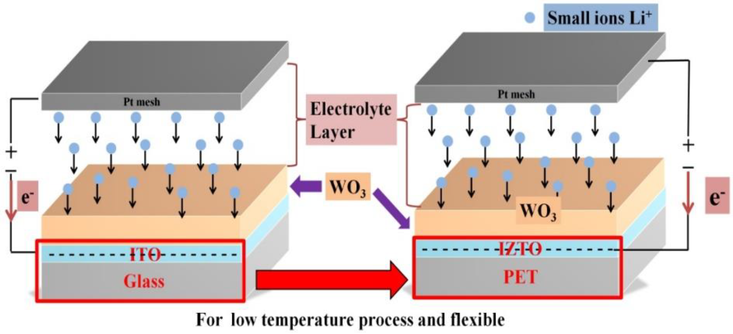
Figure 2.
The XRD patterns of the different TCO films.
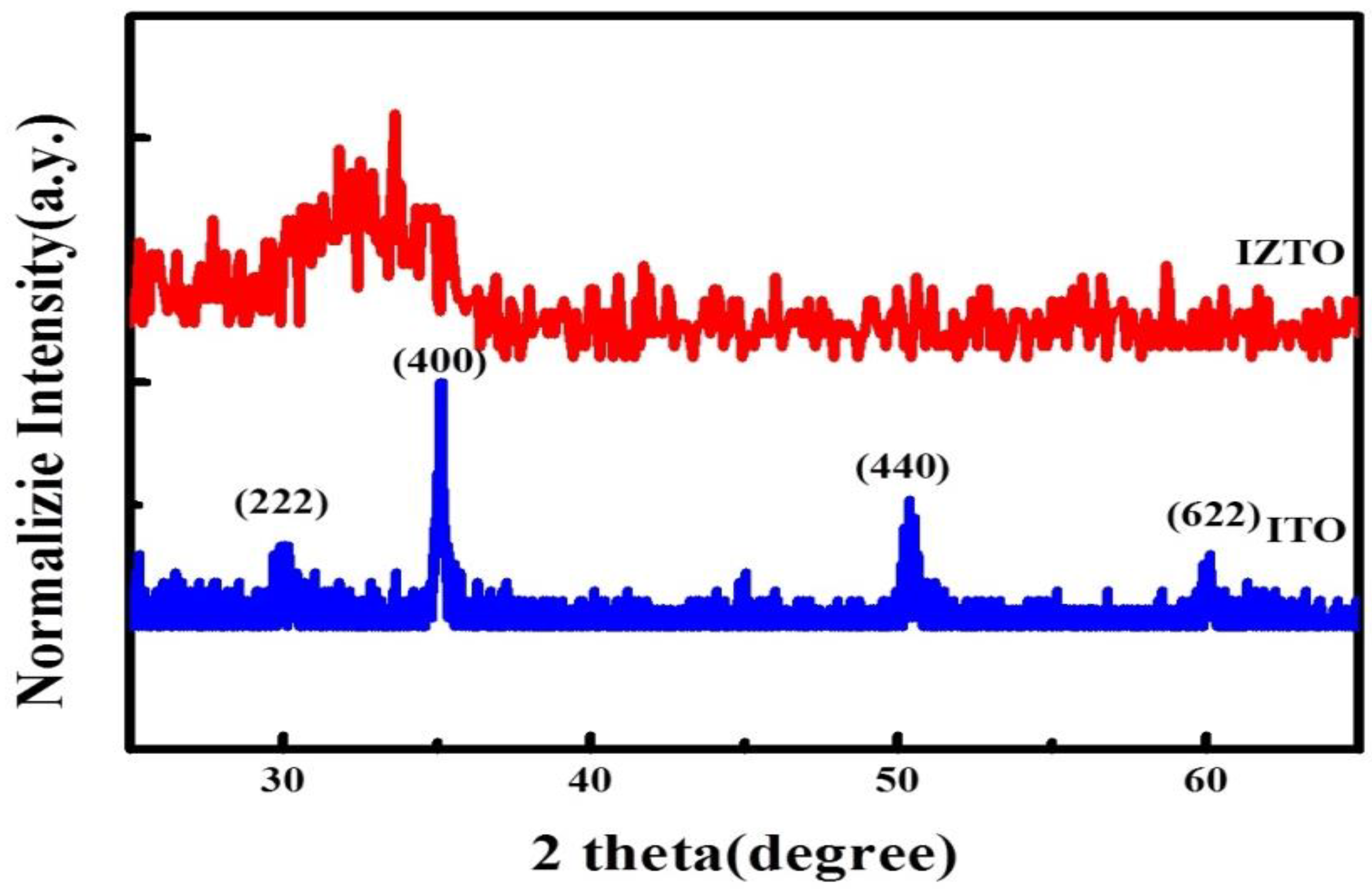
Figure 3.
The optical transmittance spectra of the different TCO films.

Figure 4.
(A) SEM images of WO3/IZTO/glass and (B) SEM images of WO3/ITO films.
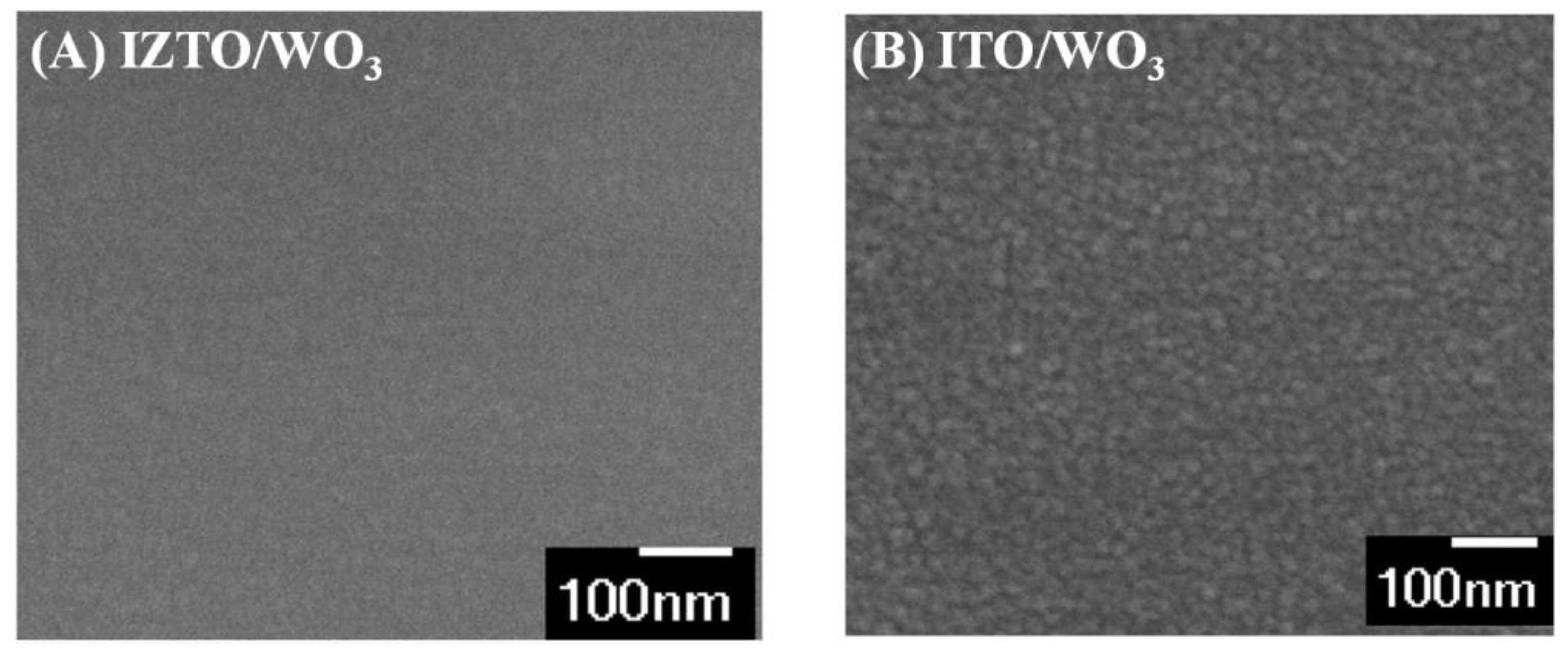
Figure 5.
The transmittance of IZTO-based and ITO-based ECDs for bleaching and coloration states.
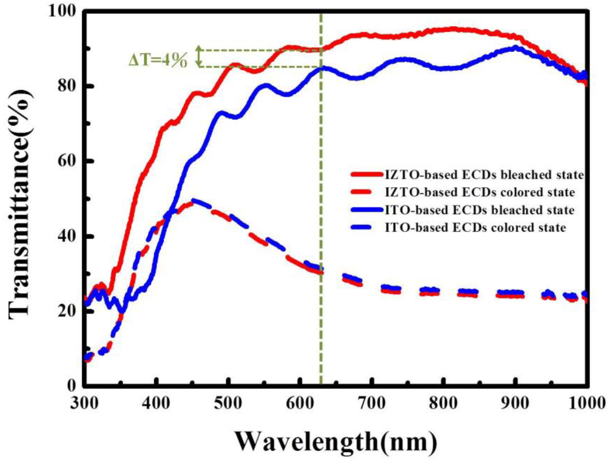
Figure 6.
Schematic diagram of electron and Li+ ions transport in the ECDs. The schematics of Li ions path through surface morphology with different grain type (a1) ITO based ECDs (a2) IZTO based ECDs. (b1,b2) Li+ ions and electrons can extract a distance of d out LixWO3, and R1 and R2 rep-resent the radius of LixWO3 particle for ITO-based and IZTO-based ECDs.
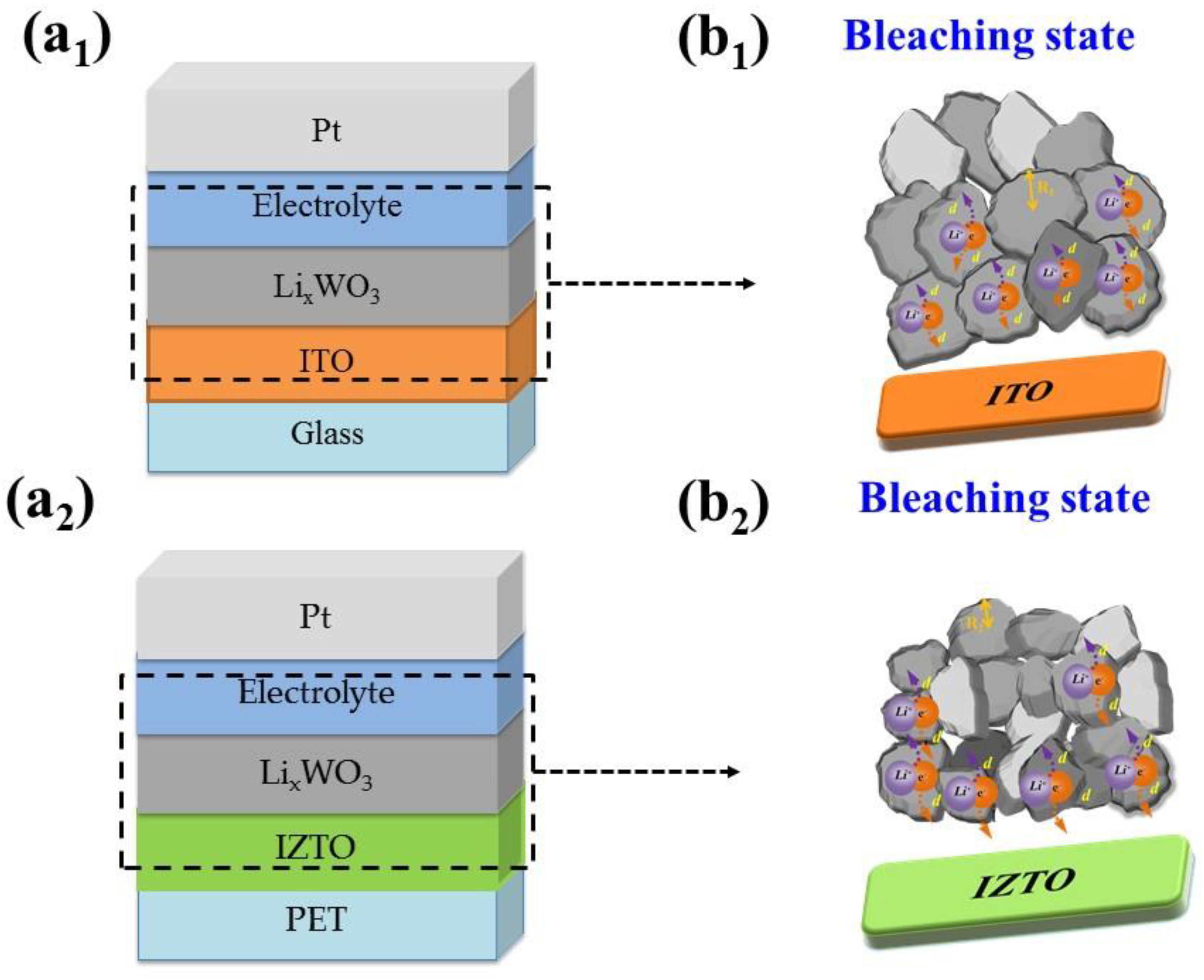
Figure 7.
(a) The current density; (b) the variation in the optical transmittance at 633 nm for IZTO-based and ITO-based ECDs.
Figure 7.
(a) The current density; (b) the variation in the optical transmittance at 633 nm for IZTO-based and ITO-based ECDs.
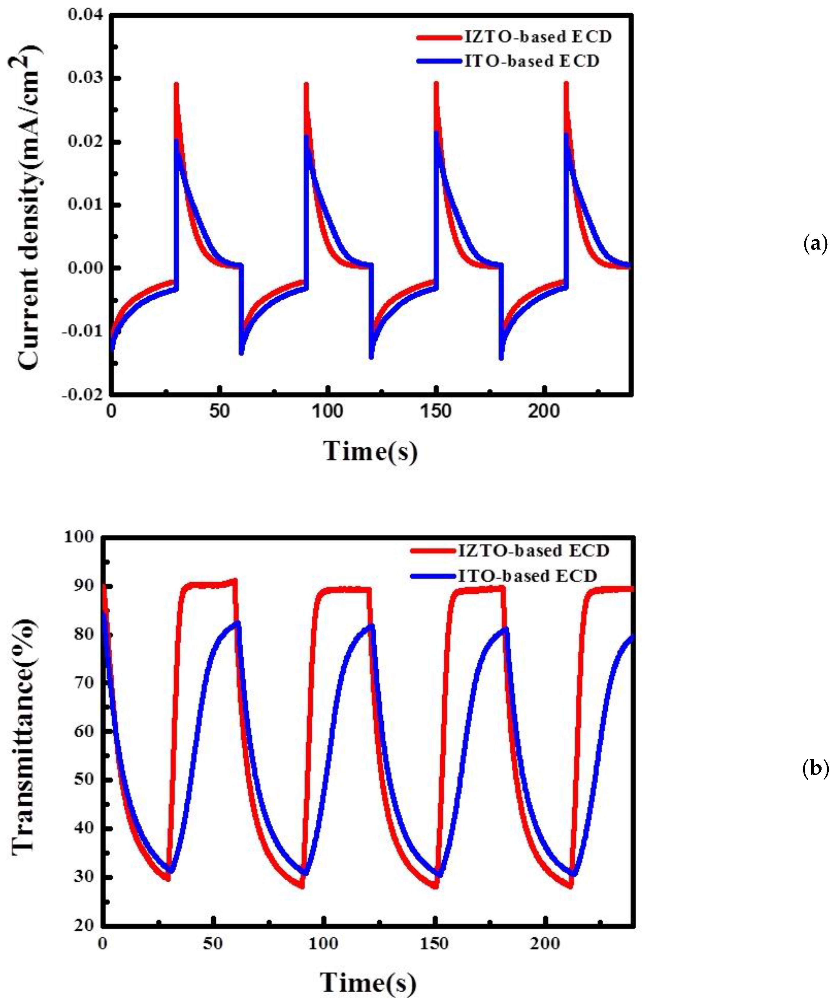
Figure 8.
A schematic of the electrochemical reaction for WO3 films in an electrolyte which is conductive by applying potential.
Figure 8.
A schematic of the electrochemical reaction for WO3 films in an electrolyte which is conductive by applying potential.
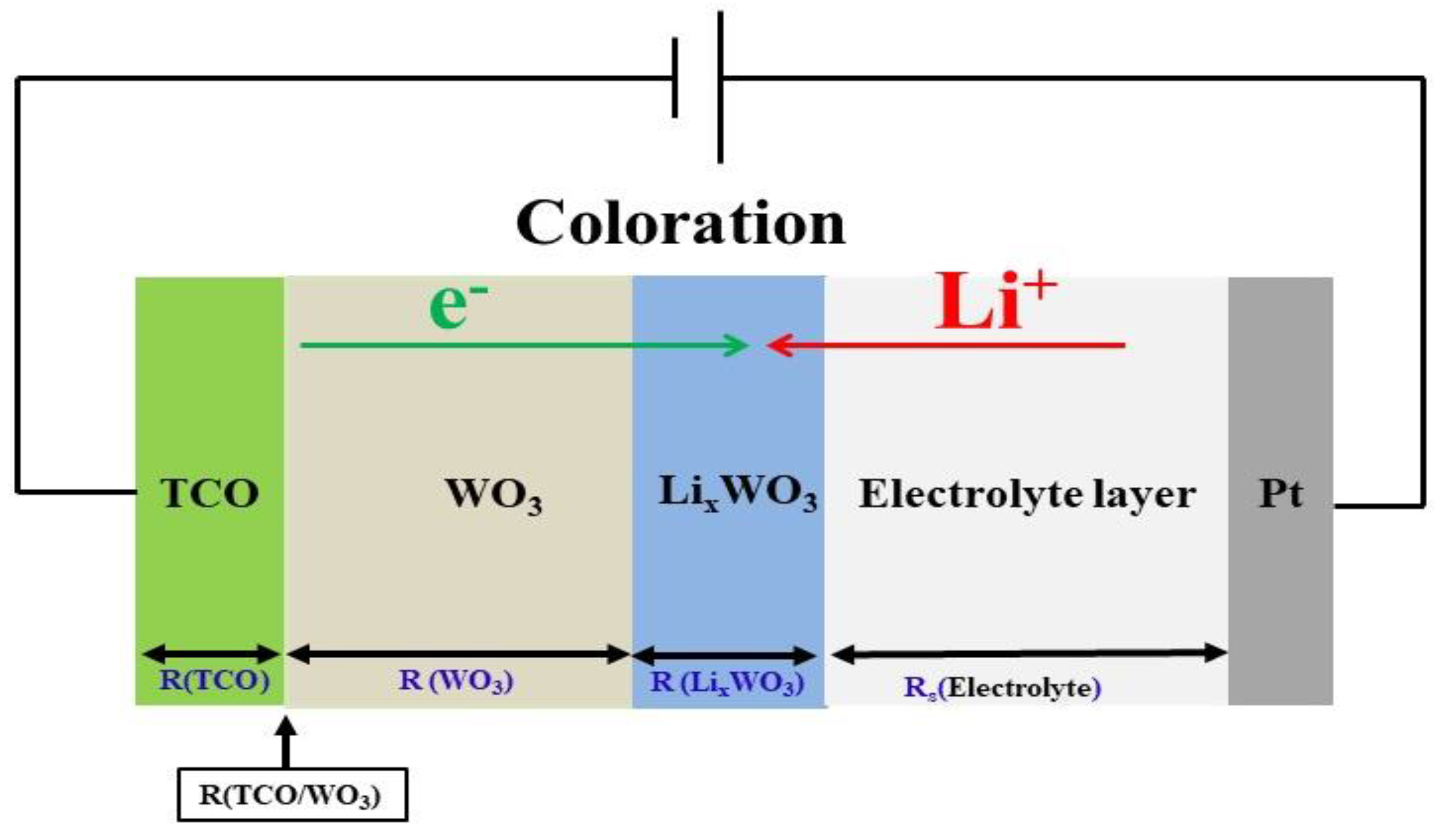
Figure 9.
Nyquist plots of IZTO-based and ITO-based ECDs.

Figure 10.
(a,c) The transmittance spectra of IZTO-based and ITO-based ECDs in the range from 300 to 900 nm using varying voltage from 0.2 V to −1.0 V. (b,d) ΔOD versus charge density at 633 nm of IZTO−based and ITO−based ECDs.
Figure 10.
(a,c) The transmittance spectra of IZTO-based and ITO-based ECDs in the range from 300 to 900 nm using varying voltage from 0.2 V to −1.0 V. (b,d) ΔOD versus charge density at 633 nm of IZTO−based and ITO−based ECDs.
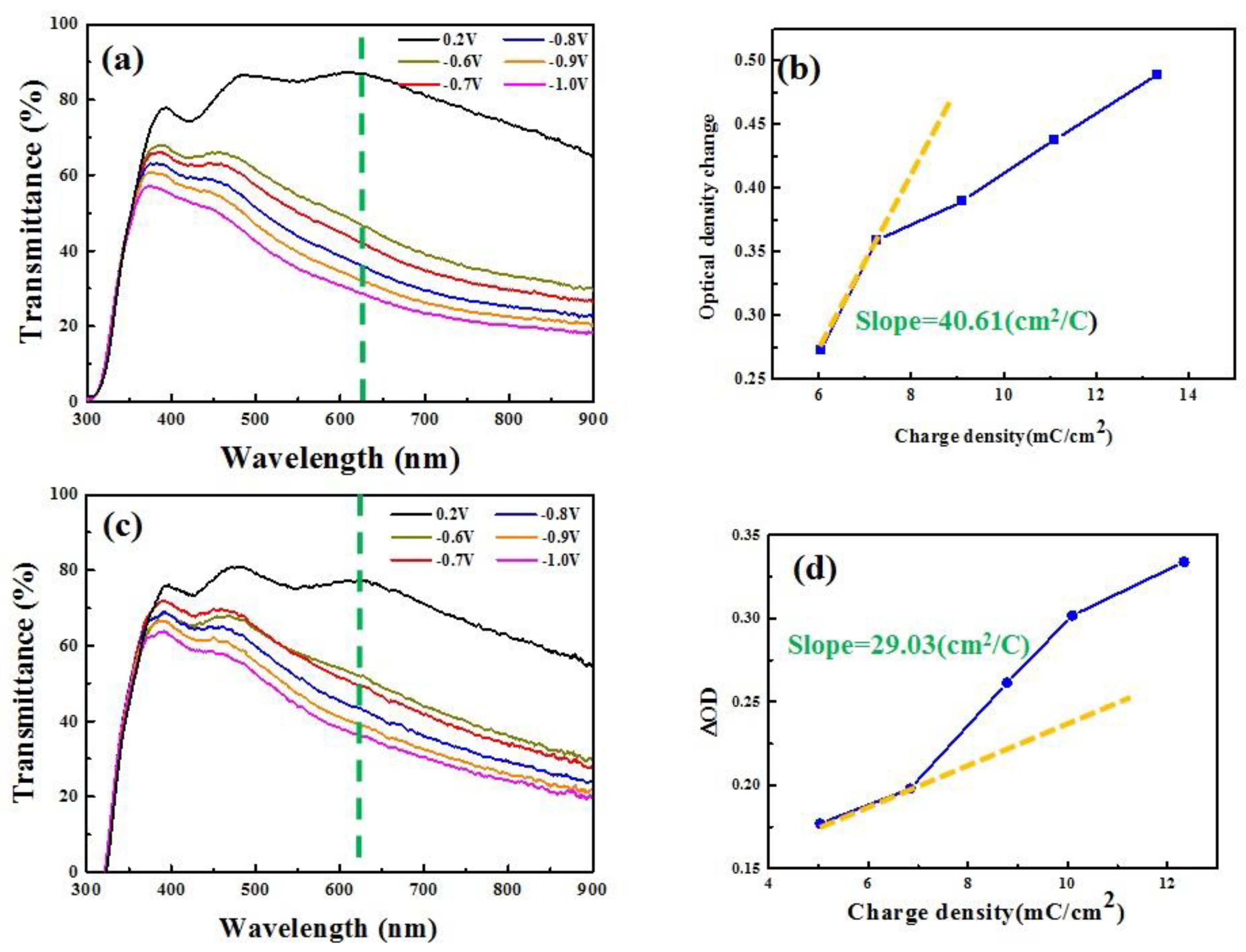
Figure 11.
Life cycle measurements for the IZTO-based ECDs by CA measurements under 0.2 V~−1.0 V for 30 s.
Figure 11.
Life cycle measurements for the IZTO-based ECDs by CA measurements under 0.2 V~−1.0 V for 30 s.


Table 1.
Details of the parameters of IZTO and ITO films.
| Processing | Working Pres. (Pa) | Base Pres. (Pa) | Ar (sccm) | DC Power (W) | Thickness (nm) | Deposition Temp. (°C) |
|---|---|---|---|---|---|---|
| IZTO | 0.13 | 9.33 × 10⁻⁴ | 30 | 100 | 800 | RT |
| ITO | 0.13 | 9.33 × 10⁻⁴ | 30 | 100 | 800 | 230 |
Table 2.
Deposition parameters of the WO3 films.
| Target | Working Pres. (Pa) | Base Pres. (Pa) | Ar/O2 (sccm) | Power (W) | Thickness (nm) | Deposition Temp. (°C) | Deposition Rate (nm/min) |
|---|---|---|---|---|---|---|---|
| Metal W | 2.7 | 1.3 × 10⁻³ | 0.2 | 1350 | 220 | RT | 14.67 |
Table 3.
The comparison of Hall measurement results, transmittance, and ΦTC values of the different TCO films.
Table 3.
The comparison of Hall measurement results, transmittance, and ΦTC values of the different TCO films.
| Processing | Transmittance (%) | Sheet Resistance (Ω/□) | Electrical Resistivity (Ω·cm) | Mobility (cm2·V−1) | Carrier Concentration (cm−3) | Figure of Merit (Ω−1) |
|---|---|---|---|---|---|---|
| IZTO | 86.8 | 7.8 | 6.2 × 10⁻⁴ | 6.622 | 8.40 × 10²⁰ | 31.1 × 10⁻³ |
| ITO | 88.4 | 7.2 | 5.7 × 10⁻⁴ | 2.95 | 2.08 × 10²¹ | 40 × 10−3 |
Table 4.
The switching response times of the coloration and bleaching states for IZTO-based and ITO-based ECDs.
Table 4.
The switching response times of the coloration and bleaching states for IZTO-based and ITO-based ECDs.
| Samples | Bleaching Time, tb (s) | Coloration Time, tc (s) |
|---|---|---|
| ITO based ECDs | 22.32 | 20.13 |
| IZTO based ECDs | 4.7 | 21.01 |
Publisher’s Note: MDPI stays neutral with regard to jurisdictional claims in published maps and institutional affiliations. |
© 2021 by the authors. Licensee MDPI, Basel, Switzerland. This article is an open access article distributed under the terms and conditions of the Creative Commons Attribution (CC BY) license (https://creativecommons.org/licenses/by/4.0/).
Share and Cite
MDPI and ACS Style
Li, K.-D.; Chen, P.-W.; Chang, K.-S. Low-Temperature Deposition of Transparent Conducting Films Applied to Flexible Electrochromic Devices. Materials 2021, 14, 4959. https://doi.org/10.3390/ma14174959
AMA Style
Li K-D, Chen P-W, Chang K-S. Low-Temperature Deposition of Transparent Conducting Films Applied to Flexible Electrochromic Devices. Materials. 2021; 14(17):4959. https://doi.org/10.3390/ma14174959
Chicago/Turabian StyleLi, Ke-Ding, Po-Wen Chen, and Kao-Shuo Chang. 2021. "Low-Temperature Deposition of Transparent Conducting Films Applied to Flexible Electrochromic Devices" Materials 14, no. 17: 4959. https://doi.org/10.3390/ma14174959
Note that from the first issue of 2016, this journal uses article numbers instead of page numbers. See further details here.