
Interface Engineering for Perovskite Solar Cells Based on 2D-Materials: A Physics Point of View


1
Department of ChiBioFarAm, University of Messina, 98166 Messina, Italy
2
C.H.O.S.E. (Centre for Hybrid and Organic Solar Energy), Department of Electronic Engineering, University of Rome Tor Vergata, 00133 Rome, Italy
3
Department of Mathematical and Computer Science, Physical Sciences and Earth Sciences (MIFT), University of Messina, 98166 Messina, Italy
*
Authors to whom correspondence should be addressed.
Materials 2021, 14(19), 5843; https://doi.org/10.3390/ma14195843
Submission received: 30 August 2021
/
Revised: 24 September 2021
/
Accepted: 29 September 2021
/
Published: 6 October 2021
(This article belongs to the Special Issue Two-Dimensional Materials in Solar Cells)
Abstract
:The last decade has witnessed the advance of metal halide perovskites as a promising low-cost and efficient class of light harvesters used in solar cells (SCs). Remarkably, the efficiency of lab-scale perovskite solar cells (PSCs) reached a power conversion efficiency of 25.5% in just ~10 years of research, rivalling the current record of 26.1% for Si-based PVs. To further boost the performances of PSCs, the use of 2D materials (such as graphene, transition metal dichalcogenides and transition metal carbides, nitrides and carbonitrides) has been proposed, thanks to their remarkable optoelectronic properties (that can be tuned with proper chemical composition engineering) and chemical stability. In particular, 2D materials have been demonstrated as promising candidates for (i) accelerating hot carrier transfer across the interfaces between the perovskite and the charge extraction layers; (ii) improving the crystallization of the perovskite layers (when used as additives in the precursor solution); (iii) favoring electronic bands alignment through tuning of the work function. In this mini-review, we discuss the physical mechanisms underlying the increased efficiency of 2D material-based PSCs, focusing on the three aforementioned effects.
1. Introduction
In the last few decades, concerns about the depletion of fossil fuels, environmental pollution and climate changes have encouraged the transition to an economy based on sustainable and renewable sources. Among these, sunlight, with a potential of 23,000 TWy/y (y = year), is the main environmental friendly source capable of meeting the current (~17.6 TWy for 2020) [1] and future (27 TWy by 2050) energy demand [2]. Nowadays, photovoltaic (PV) systems represent the most promising and mature technological solution to harness and convert solar energy into electricity. In this context, metal halide perovskites emerged as promising and outstanding PV light-harvesters for the fabrication of solar cells (SCs) because of panchromatic absorption of the visible spectrum (absorption coefficient >105 cm−1) [3,4], high charge carrier diffusion lengths (in the µm range) [3], good charge carrier mobility (24–105 cm2 V−1s−1 for MAPbI3) [3,5] and the possibility to realise thin films with low cost processing of solution precursors [6,7]. The rapid development of perovskite-based materials has its roots in the intensive research performed at the beginning of 90′s, when researchers at IBM T.J. Watson Research Center (Yorktown Heights, NY, USA) explored the optoelectronic properties of halide perovskites for commercial applications in light-emitting devices [8]. After a long silence, these materials came back on to the scene in 2009, when Kojima et al. prepared methyl ammonium lead halide (MAPbX3; where MA = CH3NH3+, X = halide anion) perovskites and investigated their optoelectronic properties [9]. Moreover, the same authors fabricated dye-sensitized SCs using MAPbX3 visible light sensitizer demonstrating good power conversion efficiency (PCE) of ~3.8%. The first report of a solid-state perovskite-based SC (PSC) appeared in 2012 with a PCE of 9.7% and 500 h stability [10]. Afterwards, the performances of PSCs increased exponentially reaching PCE of 25.5% in ~10 research years [11]. This represents a remarkable result, considering that comparable performances are shown by the well-established Si and GaAs technologies (current records of 26.1% and 27.8%, respectively) [11]. Thus, PSCs are a disruptive technology in photovoltaics due to their superb performance and potentially cheap fabrication that has pushed the PV scientific community in developing stable perovskite ink, suitable for low-cost printing techniques [6]. As the matter of fact, understanding of precursor solution chemistry is helpful to prepare high-quality perovskite films and eventually high-efficiency devices. Moreover, even if organic–inorganic perovskites are known to be defect tolerant, defect engineering at interfaces and in the bulk is important for hysteresis-free, stable and high-efficiency PSCs. In addition, a PSC is usually realized by employing a sandwiched structure composed of several components: a transparent conductive electrode (such as fluorine tin oxide—FTO or indium tin oxide—ITO), an electron transporting layer (ETL), a perovskite absorbing layer, a hole-transporting layer (HTL) and a metal contact (such as Ag, Au) [6,12]. The engineering of such a complex structure requires the development of a comprehensive knowledge of chemistry, electronic engineering, material science and physics leading to an astonishing increase in publications per year in the last decade (from 21 documents in 2012 to about 4000 in 2020, Scopus sources). Depending on the order in which the ETL and the HTL are arranged, the architecture of a PSC can be categorized as direct (n-i-p) or inverted (p-i-n) [13]. In the n-i-p configuration, titanium dioxide (TiO2) and tin dioxide (SnO2) are the most used ETL while 2,2(7,7)-tetrakis-(N,N-dipmethoxyphenylamine)9,9(-spirobifluorene)—spiro-OMeTAD—and poly[bis(4-phenil) (2,4,6,-trimethylphenyl) amine] (PTAA) represent the most common HTLs [4,12]. In the inverted p-i-n PSC, PTAA is commonly used as HTL while [6,6]-phenyl-c61-butyric acid methyl ester (PCBM) and C60 fullerene are the typical ETLs [4,12]. Furthermore, depending on the structure of the ETL, PSCs can be further classified into planar and mesoporous [13]. Specifically, the mesoporous configuration differs from the planar one for the presence of a mesoporous metal oxide layer (usually m-TiO2) between the compact hole-blocking layer (usually a compact TiO2 –cTiO2- realized by a high temperature spry pyrolysis process) or HTL and the perovskite layer [4,12].
In SCs, further PCE improvements can be realised through an optimal charge carrier transport and collection, an improved crystal growth of the layers and an optimal energy-level alignment at the interfaces. Within this context, the use of two-dimensional (2D) materials has been demonstrated as a successful strategy because of their peculiar opto-electronic properties arising from quantum-confinement effects [14]. In 2004, Geim and Novoselov isolated experimentally for the first time the forefather of 2D materials, graphene. It consists of a single layer of C atoms arranged in a honey-comb structure, characterised by a semi-metallic electronic behaviour (i.e., its band gap is 0, Table 1) and an electronic dispersion curve responsible for a relativistic-like transport of charge carriers (resulting in high charge carrier mobilities, Table 1) [15,16].
In principle, all layered crystals (i.e., characterised by strong intra-layer covalent bonds and weak inter-layer van der Waals interactions) can be easily cleaved in the corresponding 2D form [28]. Thus, through the years several 2D materials have been discovered and characterised. Among them, transition metal dichalcogenides (TMDCs) and transition metal carbides, nitrides and carbonitrides (all known as MXenes) are at the forefront of current research efforts because of their chemical stability, good charge carrier mobility (Table 1) and the possibility to tune their band gaps by varying their chemical composition [29,30]. Furthermore, several techniques are being exploited and improved for the production of high quality 2D materials, paving the way for their large scale production. Some examples are chemical vapor deposition (CVD), growth on SiC, molecular beam epitaxy, mechanical and liquid phase exfoliation, etc. [31,32].
In this work, we will present some representative results concerning the use of 2D materials in PSCs. Since this is a very hot topic in the current research trends, we do not aim to discuss the literature results (which has been reviewed by several interesting papers) in depth [33,34,35,36], but to highlight some physical mechanisms behind the successful implementation of 2D materials within the PSCs structure. In particular, the discussion will cover the effects on: (i) hot-carriers; (ii) crystallization of the perovskite layer and (iii) tuning of energy levels. Thus, our work will give a first idea of the promises and advantages in synergistically using such technologies for improved PV performance.
2. The Family of 2D Materials
Graphene, the first 2D material isolated in 2004 by Geim and Novoselov, consists of a single layer of sp2 hybridized C atoms arranged in a honeycomb crystal lattice (Figure 1a).
The quantum nature of 2D materials leads to peculiar physico-chemical properties. For example, graphene is a zero-bandgap semi-metal (its valence and conduction bands meet at the Dirac point) with an ambipolar electrical transport behaviour showing charge carrier mobilities as high as 2∙104 cm2 V−1 s−1. A graphene single layer exhibits a high transparency (97.7% in the visible range) [40,41] resulting in a promising material for the replacement of transparent conductive materials such as ITO and FTO. In addition, graphene has an elastic limit of ~20% and a weight of only 0.77 mg m−2, making it a suitable material for the realisation of flexible and light devices [42,43]. Finally, it is worth mentioning that graphene’s properties can be changed by chemical functionalization with oxygen-containing groups. For example, pristine graphene is hydrophobic (thus it cannot be well dispersed in water) [44], however the oxidation of graphene to graphene oxide (GO) permits uniform dispersion in aqueous solutions thanks to the introduction of many functional hydrophilic groups (like epoxide and hydroxyl groups on the planar surface and carboxylic groups at the edges) [45]. However, because of the distortion of the sp2 conjugation of the hexagonal graphene lattice induced by the presence of covalent C–O bonds, GO is an insulator [46]. Nevertheless, after chemical reduction processes GO is transformed into reduced graphene oxide (rGO) that is characterized by high conductivity and transparency resulting in an attractive and promising material for optoelectronic applications [47]. Figure 1b,c schematically represents the crystal structure of GO and rGO, respectively. The TMDCs are a large family of 2D materials with chemical formula MX2, where M is a transition metal atom (such as Mo, W, Ta, Nb, etc.) and X is a chalcogen atom (for example S, Se or Te) [48]. Specifically, a TMDC single layer consists of a plane of metal atoms sandwiched between two layers of chalcogen atoms. The intralayer M–X bonds are covalent, while adjacent layers of TMDs (in bulk form) are weakly bonded to each other by Van der Walls interactions forces, enabling exfoliation into single layers [48]. Depending on the specific chemical composition, 2D-TMDCs can exist in two different structural phases, the octahedral (1T) and trigonal prismatic (2H) ones (Figure 1d–f). In the notation 2H and 1T, the number indicates the X-M-X units (i.e., the number of layers in the unit cell) while the letter denotes the hexagonal (H) and trigonal (T) symmetries [30,48,49]. According to the chemical composition and depending on the progressive filling of the orbitals, TMDCs can have different opto-electronic behaviour: semiconductors (i.e., MoS2, WS2), metals (i.e., NbS2, VSe2), semimetals (i.e., WTe2, TiSe2) and insulators (i.e., HfS2) [30,48,49]. In particular, the TMDCs formed by group-VI transition metals (i.e., MoS2, MoSe2, WS2 and WSe2) are widely used for electronic and opto-electronic devices thanks to their charge carrier mobilities (up to 500 cm2 V−1 s−1 in WSe2) [17] and bandgaps (ranging from the near-infrared to the visible electromagnetic spectrum) [50,51,52]. Finally, another interesting group of 2D materials is represented by MXenes. Their 3D precursors are characterised by the chemical formula Mn+1AXn (where M is a transition metal, A is mainly an element of the 13 or 14 group of the periodic table, X is a C and/or N atom, n+1 and n are the numbers of M and X layers, respectively, with n = 1–3); the associated structure is reported in Figure 1g. The 2D form of these materials are produced by etching the A layers [53,54]. After the etching process, the A layers are replaced by surface terminations (indicated with Tx) such as OH, O and F and so MXenes with chemical formula Mn+1XnTx are synthesized [53,54]. Interestingly, MXenes offer the possibility to tune their optoelectronic properties by choosing properly their chemical composition. For example, their functionalization causes variations of the electrostatic potential near the surfaces, affecting the electronic structure and work function (WF) from 1.6 eV (for OH termination) to 6.25 eV (for O termination) [29,34,55]. These features make MXenes very interesting for the production of SCs; as demonstrated by the Ti3C2Tx,the most used material within this family, showing exceptional properties such as high electronic conductivity (6500 S cm−1), modest mobility (0.9 cm2 V−1 s−1), and high charge carrier density (3.1∙1022 cm−3) [56].
3. Effects of 2D Materials on Hot Carriers
In PV devices, charge carriers are produced after absorption of photons with energies equal to or far above the bandgap of the light harvester. In the latter case, the photo-generated electrons and holes will populate states above the conduction band minimum (CBM) and below the valence band maximum (VBM), respectively, which are referred to as hot carriers (HCs) [57]. If such HCs can be collected before bringing themselves to thermal equilibrium with the lattice, it is possible to push the PCE of a SC to ~66% (exceeding the Shockley–Quiesser limit of 33% for a single junction SC) [57]. The main issue for the practical realization of HCs based SCs is that HCs relax in an ultrafast timescale, losing the excess energy through two mechanisms: thermalization and cooling [58]. The thermalization process, which occurs within 100 fs, consists in the exchange of energy between carrier–carrier scattering until the HCs reach an equilibrium condition (according to the Fermi–Dirac distribution) with a characteristic temperature TC [58,59]. In the cooling process, which occurs within 1 ps, the HCs reach thermal equilibrium with the lattice via carrier–phonon scattering [58]. It is worth emphasizing that the HC cooling is one of the main causes for the PCE loss in a SCs (for example ~25% for a MAPbI3-based PSCs) [58]. Interestingly, perovskites emerged as promising absorbing material for the realization of HC-based SCs because of the higher HC cooling lifetime (<6 ps for MAPbI3, 37 ps for CsPbIBr2, 71 ps for MAPbBr3 and 305 ps for FAPbI3) [60] with respect to other semiconductors (1.4 ps for InN and 2 ps for GaAs) [61,62]. However, it should be mentioned that in addition to large HC cooling lifetimes, energy-selective contacts are necessary for the extraction of the HCs [59]. These energy-selective contacts act as energy filters extracting only carriers with a narrow range of energies and preventing cold carriers (from the external contacts) from cooling HCs [59,63]. In the last few years, 2D materials and particularly graphene rose as potential candidate for the production of energy-selective contacts for efficient charge carrier collection, including HCs [64,65,66].
For example, O’Keeffe et al. [64] demonstrated that the incorporation of graphene flakes in the m-TiO2 based ETL of a PSC is advantageous for the extraction of the HCs allowing the stability and the PCE of mesoporous-based devices to be improved (Figure 2a shows the whole investigated architecture).
In particular, the authors used transient absorption spectroscopy (TAS) to study the dynamics of the carriers within PSCs before and after 1 week of aging. Figure 2b displays the false colour map of the TA spectra as a function of the probe energy and pump-probe time delay for the as-prepared graphene-based PSC (PSC-G). The TA map presents two positive regions ascribed to the photoinduced absorption (PIA1 and PIA2) of MAPbI3 and two negative regions attributed to photobleaching (PB1 and PB2). Figure 2c shows the comparison of the TAS characterization, in the PB1 region, performed on as-prepared PSC-G and reference sample (i.e., without any graphene—PSC-NoG); while Figure 2d reports the spectra measured after aging of the same samples. The focus on the PB1 contribution is due to the fact that it represents the only one providing information about the occurring physico-chemical processes (indeed the other regions show only slight variations of the optical density). A more detailed analysis of Figure 2c,d reveals that there are two distinct peaks in the PB1 region, which the authors assigned to the absorption bleaching of large perovskite crystals (of the absorbing layer, PB1A centred at 1.64 eV) and in small perovskite crystals (infiltrated within the m-TiO2 layer, PB1B at 1.66 eV). Moreover, it is worth noting that the relative intensities of the PB1A and PB1B peaks of the PSC-G sample are the same for the as-prepared device and after aging. By contrast, for the aged PSC-NoG an evident reduction of the relative intensities of PB1A and PB1B is observed with respect to the as-prepared sample. According to the authors, these results suggest that the use of graphene in the m-TiO2 layer hinders the degradation of small crystals by avoiding the iodine diffusion from the perovskite in the ETL. Furthermore, as observed in Figure 2d, the photobleaching signal of the PSC-G is wider compared to that of the PSC-NoG. In order to explain this behaviour, it should be mentioned that the shape of the high-energy tail (of Figure 2c,d) is linked to the TC. In particular, TC values can be obtained from the TA spectra by fitting the high energy tails with a Maxwell–Boltzman distribution. The TC as functions of the time delay for the as-prepared and aged PSC-NoG and PSC-G samples are shown in Figure 2e,f. Figure 2e reveals a two-component exponential decay of TC for both as-prepared PSC-NoG and PSC-G, characterised by a comparable starting TC (1650 and 1800 K, respectively) and decay lifetimes (the authors obtained, for both samples, values of ~400 fs and 15–20 ps for the two exponential components). Thus, the use of graphene gives only slight variations to the starting HC temperature and decay lifetimes, for the as-prepared samples. On the contrary, Figure 2f shows that PSC-NoG and PSC-G exhibit different starting TC (1300 K and ~1800 K, respectively) after 1 week of aging but similar two-components decay dynamics with respect to the as-prepared counterparts (~480 fs and 23 ps for the PSC-NoG case, ~420 fs and 15 ps for the PSC-G case). For this reason, the authors propose that graphene acts as a shield for the starting TC preserving small perovskite crystals (in the m-TiO2 layer) from degradation, while in the absence of graphene this contribution is lost (thus charge-carriers suffer from a faster thermalization).
A very interesting study was reported by Hong et al. [65], who performed tunable two-colour pump-probe TAS measurements in combination with theoretical calculations to investigate the HCs dynamics on MAPbI3 perovskites grown onto a graphene layer. Interestingly, the authors prepared a clean graphene layer through chemical vapour deposition (CVD), without the need of any polymer-based transfer procedure. Afterwards, a very thin (~10 nm) MAPbI3 crystal was grown on top of the clean graphene through a one-step solution process (i.e., by putting in contact the graphene surface with a solution of CH3NH3I and PbI2 salts). The 2D map of the TAS signal of the clean graphene/MAPbI3 interface, at different probe wavelengths and pump–probe delay times, is shown in Figure 3a, revealing an absorption peak centred at 680 nm.
The vertical cut of the 2D map at 680 nm (Figure 3b) provides the decay of the bleaching signal. Figure 3c shows a restricted range of Figure 3b, together with a measurement performed on a dirty graphene/MAPbI3 interface (i.e., graphene grown by CVD and transferred by using a polymer). According to these results, the rising part of such spectra indicates a faster charge carrier collection for the clean graphene/MAPbI3 interface (~100 fs) with respect to the dirty graphene/MAPbI3 one (~530 fs). However, it is fundamental to assess the charge carrier collection efficiency (η) to exclude that charge carriers suffer from trapping phenomena in such hetero-structure. For this reason, the authors performed time-resolved photoluminescence spectroscopy measurements on pristine MAPbI3 and on the hetero-structures formed with clean and dirty graphene (Figure 3d), obtaining η = 98.7% for the clean graphene/MAPbI3 case and 97.7% for dirty graphene/MAPbI3 sample. Although these results are quite similar, it should be emphasised that the efficient collection of HCs must be realised in the ps time-scale, so slight variations of η can make a remarkable difference. Indeed, comparisons of TAS measurements performed on clean graphene, MAPbI3 and clean graphene/MAPbI3 interface (Figure 3e) reveal the superior HCs collection of the hetero-structure since the peak observed in this characterization is six times higher with respect to the pristine graphene case. Finally, the authors performed time-dependent density functional theory calculations of the charge collection time of carriers at different energies, observing a good agreement with their experimental data (Figure 3f).
In a following work, the same group conducted further studies on an identical heterostructure with the aim to shed light on the HCs dynamics [66]. Figure 4a–c illustrate the schematic representation of the three possible pathways proposed by the authors to describe the HCs dynamics at MAPbI3/graphene heterostructure.
In the first case (pathway1, Figure 4a) the hot electrons (HEs) on the MAPbI3 layer relax to the CBM and then diffuse to graphene. For the second process (pathway 2, Figure 4b) firstly, the hot electrons transfer from MAPbI3 to graphene and then relax to the graphene Dirac point. Finally, there is an additional process (pathway 3, Figure 4c) in which the hot electrons follow a zigzag walk between the two layers (perovskite and graphene) that form the heterostructure. To identify the pathway followed by HCs, the authors performed a direct non adiabatic analysis and studied the dynamics of HEs with energies of 2.9 and 3.2 eV above the Fermi level of the heterostructure. As shown in Figure 4d, firstly the HEs transfer to graphene in less than 20 fs (the population at graphene of excited HEs increases). After that, the HEs travel back to MAPbI3 (there is a drop of the charge population on graphene) on a time scale of ~75 fs (a similar behaviour was already observed in graphene/WS2 heterostructure) [67]. Finally, the HEs diffuse from MAPbI3 to graphene causing an increase of the population on graphene to 86%. These results indicate that the dynamics of the HCs at MAPbI3/graphene interface is described by pathway 3. The overall process takes place on a time scale of ~400 fs that is in good agreement with previous experimental observations that predicted an ultrafast charge collection time of ~100 fs at the graphene/MAPbI3 interface [65].
The presented results, although very interesting, concern a very particular case: the interface between CVD graphene and a thin (~10 nm) perovskite crystal. However, in practical devices, perovskite layers usually reach a thickness of hundreds or thousands of nm, thus the straightforward translation of these results into a realistic scenario is not trivial. Further research on this field is fundamental to assess the practical implementation of such a strategy for the realization of HC-based PSCs.
4. The Role of 2D Materials in the Growth of High Crystalline Quality Perovskite Films
The crystalline and morphological quality of a perovskite film plays a key role for the realization of PV devices with high performance [68]. Specifically, in order to fabricate a PSC with a high PCE and a good stability, it is important to grow a perovskite layer that is uniform and smooth with a low amount of defects (to avoid the presence of a large number of recombination centres and loss of voltage) and large grain size (that favours an efficient transport of charge carriers to the electrodes) [69,70,71,72,73]. With the aim to improve the perovskite film quality, that depends on the preparation method used (such as one or two step solution process, co-evaporation or spin coating) [74,75,76] and other factors (for example the choice of the solvent or the precursor composition and annealing treatment) [77,78,79], several approaches including new deposition technologies [80,81], post-treatment [82] and additive engineering [83,84] have been proposed. In particular, the use of 2D materials within the perovskite precursor solution represents a promising route to control the nucleation and growth processes of perovskite films.
For instance, Gidey et al. used chlorine functionalized GO (Cl-GO) as additive into a MAPbI3 precursor solution, resulting in high quality of the perovskite layer and leading to improved PCE of the device compared to the pristine MAPbI3 based PSC [85]. To study the structure and the morphology of MAPbI3 with different amounts of Cl-GO (1.0 vol%, 2.0 vol%, 5.0 vol% and 7.5 vol%) the authors performed X-ray diffraction (XRD) and scanning electron microscopy (SEM) measurements and compared the results with that of pristine MAPbI3. The XRD results (Figure 5a) show two main characteristic peaks at 14.2° and 28.4°, corresponding to the crystallographic planes (110) and (220). Remarkably, for all the samples there is no shift of the peaks positions, indicating that both pristine MAPbI3 and MAPbI3-Cl-GO films share the same crystalline structure, however several variations in the shape and intensity of the pattern are observed (underlying different crystallite dimensions, in accordance with Sherrer’s relation). In fact, Figure 5b-f report the SEM images of both pristine MAPbI3 and MAPbI3 films prepared with different amounts of Cl-GO, confirming that grain size increases with the addition of Cl-GO up to 5.0 vol% concentrations. However, with higher Cl-GO concentration (7.5 vol%) the perovskite film was subjected to the formation of cracks within the grain boundaries that has a negative impact on the performances of the PSC. Indeed, the PCE of the devices fabricated by the authors is boosted from 12.81% to 15.14% by increasing the amount of Cl-GO from 0.0% to 5.0% and decreases to 14.16% in the case of MAPbI3-Cl-GO 7.5 vol% based PSC. Thus, these results reveal that the proper addition of Cl-GO has a beneficial impact on the nucleation and crystal growth processes of metal halide perovskites.
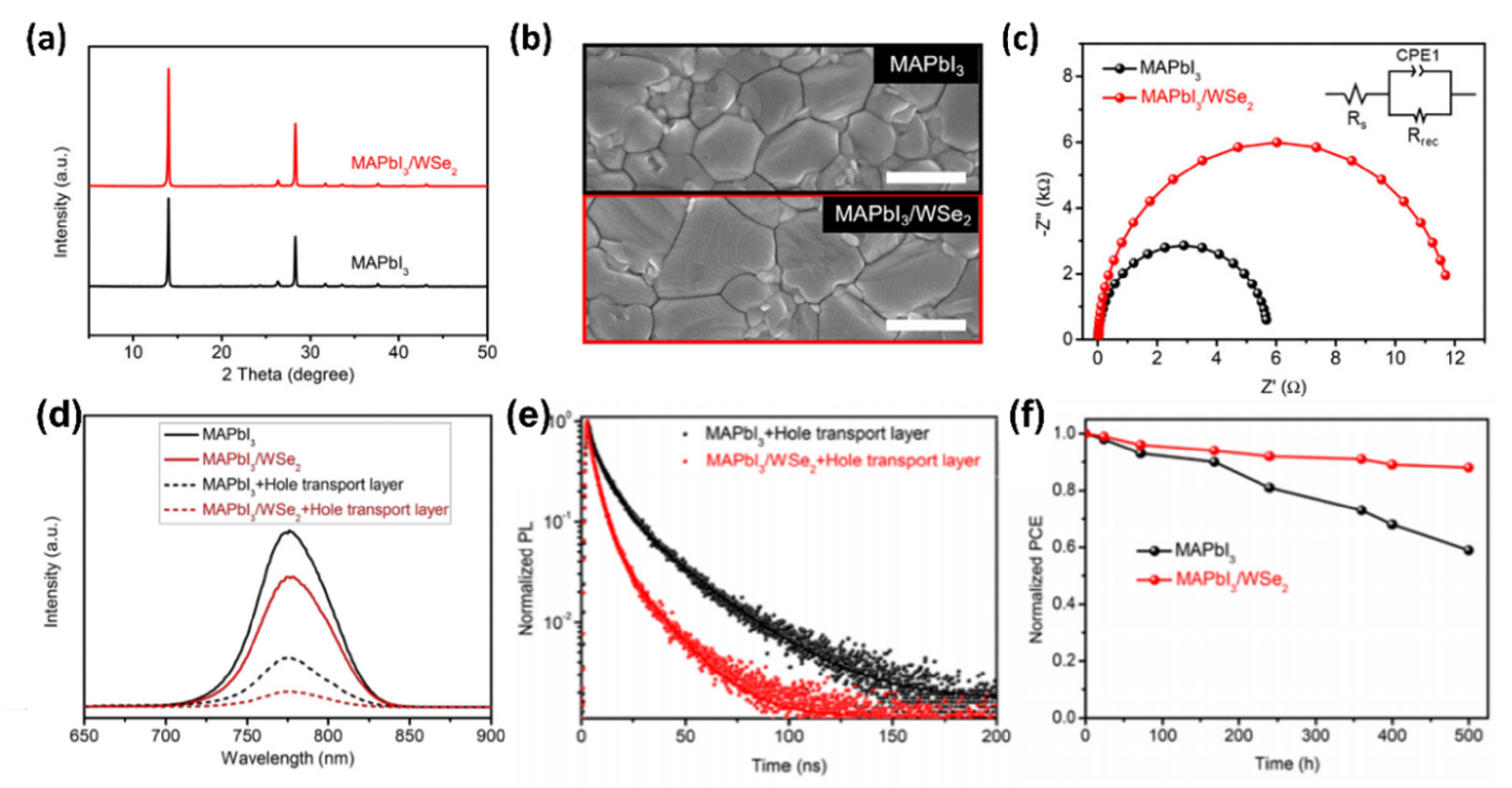
Similar results in the improvement of the crystallization process to obtain high-quality perovskite films with uniform morphology and large average grain size were obtained by Qin et al. [86] through the addition of quasi-monolayer WSe2 nanosheets into MAPbI3 precursor solution. The average thickness of the quasi-monolayer WSe2 nanosheets (synthesized by liquid phase exfoliation) is ~0.8 nm (the same thickness values are reported for a monolayer of WSe2). Specifically the role of WSe2 in the growth of MAPbI3 film was investigated by using XRD and SEM techniques (Figure 6a,b).
In particular, as shown in Figure 6a, the MAPbI3-WSe2 film displays the same XRD features, ascribed to MAPbI3 crystals (with the main peaks located at 14.2° and 28.4°) [85]. Furthermore, in both XRD spectra no relevant shift of the position of the peaks is observed, indicating that after the introduction of WSe2 into the MAPbI3 precursor solution the crystal structure of the perovskite is not altered. Significantly, the relative intensities of the peaks of the MAPbI3/WSe2 layer are higher compared to those of the pristine MAPbI3 film, suggesting an enhanced crystalline quality. Figure 6b presents the SEM images of the MAPbI3 and MAPbI3/WSe2 films, respectively. The average crystal size is larger for the MAPbI3/WSe2 sample, confirming that WSe2 is an effective additive for controlled nucleation and growth of perovskite films. Moreover, to truly understand the charge carrier transport and recombination behaviour, the authors conducted electrochemical impedance spectroscopy (EIS) measurements. The Nyquist plots of the MAPbI3 and MAPbI3/WSe2-based PSCs are depicted in Figure 6c (in the inset the equivalent circuit model is represented). In these plots the semi-circles in the high and low frequency regions are assigned to the recombination resistance (Rrec) and series resistance (RS) respectively. In particular, by fitting the Nyquist plots, Rrec values of 12 kΩ and 6 kΩ were obtained for the MAPbI3/WSe2- and MAPbI3-based PSCs, implying that the WSe2 nanosheets suppressed the charge carrier recombination. In addition, the charge carrier extraction properties were analysed by both steady state PL and TRPL experiments. As shown in Figure 6d, the PL intensity of the MAPbI3/WSe2 layer with the HTL deposited on top is lower than that of the other structures examined, resulting in an improved hole extraction ability and confirming the reduced charge carrier recombination induced by the WSe2 nanosheets. This result is also supported by the trend of the TRPL decay curves of both MAPbI3+HTL and MAPbI3/WSe2+HTL structure (Figure 6f). Indeed, a faster decay is observed for the MAPbI3/WSe2+HTL sample underlying again the beneficial role that the WSe2 has in the hole transport. Finally, the stability of both MAPbI3 and MAPbI3-WSe2-based PSCs was investigated and the result is shown in Figure 6g. It is clear that the MAPbI3/WSe2-based PSC retains 91% of its initial PC) after storage in a N2 glovebox for 500 h under continuous illumination (100 mW cm−2 white LED), while the reference MAPbI3 based PSC suffers from severe degradation with a PCE retention of 60% under the same aging conditions. The enhanced stability of the MAPbI3/WSe2-based PSC is attributed by the authors to the passivation of Pb0 defect due to the formation of Pb-Se coordination bonds between WSe2 and MAPbI3.
5. The Role of 2D Materials for Electronic Energetics Tuning and Interface Engineering in Perovskite Solar Cells
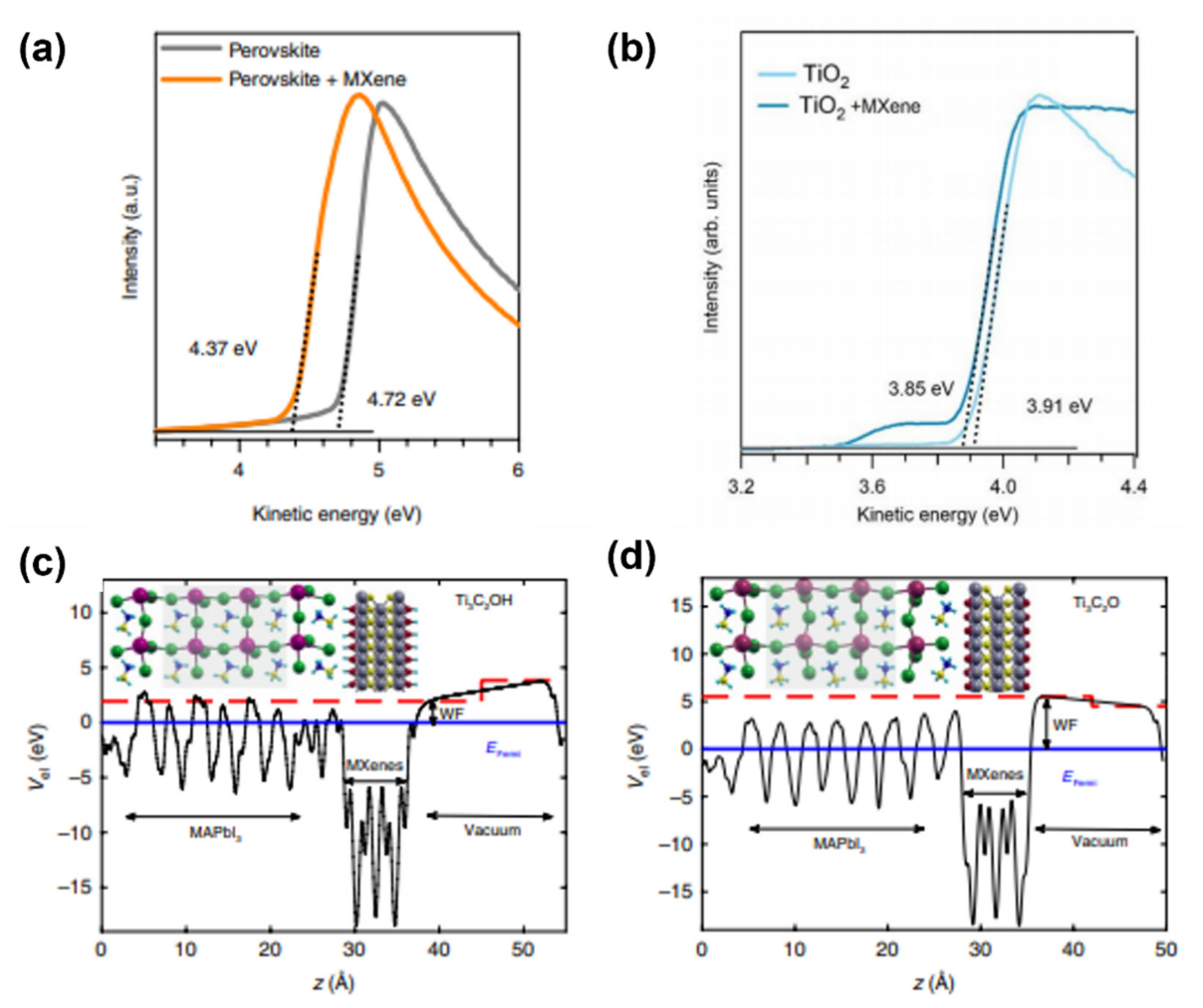
In a PSC, the absorbing layer is sandwiched between the ETL and the HTL, and thus one of the most important prerequisites to achieve high performance is the optimal alignment of the energy levels at the interfaces. Since 2D materials exhibit a tunable electronic structure by varying their chemical composition or functionalization, they hold great promises for engineering such interfaces. In this regard, Agresti et al. used Ti3C2Tx as an additive within a triple cation perovskite and TiO2, with the aim to tune the corresponding WFs. Ultraviolet photoemission spectroscopy (UPS) measurements (Figure 7a,b) reveal a shift of WF from 4.72 to 4.37 eV (for perovskites) and from 3.91 to 3.85 eV (for TiO2). In the case of the doped-TiO2, the slight WF variation is due to the partial oxidation of MXene during the annealing necessary for the TiO2 sintering process. To shed light on the mechanisms underlying the WF changes in the doped-triple cation perovskite, the authors performed density functional theory (DFT) calculations of a doped-MAPbI3 structure considering OH and O terminations. Calculations were performed by using MAPbI3 to make the computation feasible and because the same WF shift was also observed for such perovskite. The results are shown in Figure 7c,d that reveal the formation of a dipole at the MAPbI3/Ti3C2Tx interface, thus the WF tuning arises from electrostatic effects. The same result was obtained for simulated doped-FAPbI3, while for the case of doped- CsPbI3 the WF is expected to be higher because of the larger band gap of Cs-based perovskites. Thus, for the triple cation perovskite used by the authors, an overall reduction of the WF is expected (since Cs constitutes only the 5% of the overall inorganic cation concentration).
Due to the possibility to play with MXenes terminations during their chemical synthesis, theoretically the whole phase-space of F, OH, and/or O mixtures [87] could be explored in combination with different perovskite compositions, opening the way to a general approach for engineering optoelectronic devices based on a perovskite active layer. Moreover, the proposed strategy is suitable for different PSC structures. Indeed, when applied in mesoscopic n-i-p architecture, the reduction of perovskite WF mediated by the Ti3C2Tx MXenes was effective for reducing the valence band barrier at the perovskite/spiro-OMeTAD interface, leading to an increased open circuit voltage (VOC). A similar engineering strategy was recently reported for inverted p-i-n architecture where a MXene-doped MAPbI3 absorber was grown over a NiOx HTL and topped with a PCBM/BCP/Ag negative electrode [88]. Notably the same MXenes precursor was here used to dope both perovskite and PCBM layers, in order to engineer the energy level alignment at MAPbI3/PCBM interface while improving the charge dynamics within the whole device structure. Indeed, a Ti3C2Tx with the ratio ~1 between ‒OH to ‒O terminations was selected for achieving 4.35 eV WF value, suitable for inducing a negative shift in both MAPbI3 and PCBM materials, responsible for a remarkable enhancement in the photocurrent generation, considering the red-NIR part of the visible spectrum. The as-modified inverted PSC achieved efficiency above 19%, a remarkable result when considering the standard p-i-n architecture based on NiOx HTL and MAPbI3 without adding complexity to the cell fabrication process as in the case of additional interlayers or passivation steps. As a matter of fact, the interface engineering based on MXenes was demonstrated as an effective tool in boosting the performance of PSC employing a fully inorganic CsPbBr3 perovskite active layer and carbon electrode, aiming for a long lifetime under real working condition [89]. In particular, Ti3C2-MXenes were inserted as an interlayer between perovskite and carbon top electrode (FTO/TiO2/CsPbBr3/Ti3C2/carbon) for eliminating the energy level mismatch, by accelerating the hole extraction and reducing the recombination at the interface. Moreover, the nanosheets MXene functional groups such as ‒O also provide strong interactions between the MXenes and under-coordinated Pb atoms, which led to a remarkable reduction of the deep trap defect concentration in the CsPbBr3 films. Notably, the MXene-engineered carbon-based cell demonstrated long-term stability for over 1900 h in a moisture environment and more than 600 h under thermal conditions, by ensuring PCE above 9%.
Figure 7.
UPS spectra of (a) MAPbI3 and (b) TiO2 doped with Mxenes. Results of DFT calculations concerning the electrostatic potential of planes perpendicular to the (c) MAPbI3/Ti3C2(OH)2 and (d) MAPbI3/Ti3C2O2 interface. Data taken from ref. [90]. Copyright Springer Nature@2019.
Figure 7.
UPS spectra of (a) MAPbI3 and (b) TiO2 doped with Mxenes. Results of DFT calculations concerning the electrostatic potential of planes perpendicular to the (c) MAPbI3/Ti3C2(OH)2 and (d) MAPbI3/Ti3C2O2 interface. Data taken from ref. [90]. Copyright Springer Nature@2019.
6. Promises and Challenges for the Large-Scale Use of 2D Materials in PSCs
With these premises, the interface engineering strategy based on 2D materials could assume a pivotal role in the future in pushing the development of commercialization of perovskite-based solar cells, still hampered by the not unequivocally demonstrated device stability and difficult device scalability. Indeed, as main concern, the astonishing results in terms of PCE demonstrated over lab-scale devices are still far from being equalled by large-area modules, while stability under established stress test protocols [91] was not still fully addressed. To this extent, Agresti et al. [92] recently reported a valuable example of interface engineering strategy based on 2D materials and applied to a perovskite large area module [93,94]. More in detail, the easy tuning of 2D material optoelectronic properties is here exploited for shifting the MoS2 valence band edge that does not perfectly match with the perovskite highest occupied molecular orbital (HOMO) level and possibly forms an energy barrier for the hole extraction process. The MoS2 energy bands up-shift was obtained by linking the thiol group of 3-mercaptopropionic acid moieties to the MoS2 surface via S−S van der Waals physisorption and/or S-vacancy passivation. Once engineered in terms of energy band, the as-functionalized MoS2 (fMoS2) was inserted as interlayer at perovskite/HTL interface with the double role to improve the hole extraction process (by reducing the potential barrier at the perovskite/HTL interface), while restricting the undesired electron transfer from perovskite (since the conduction band edge of MoS2 above the LUMO level of the perovskite proves electron blocking properties). When fMoS2 was inserted as interlayer in a device structure employing even graphene-modified photo-electrode (FTO/cTiO2+G/mTiO2+G/perovskite/fMoS2/spiro-OMeTAD/Au), modules with 13.4% PCE were demonstrated with an active area larger than 108 cm2. Here, the rational use of 2D materials allows the PCE efficiency gap usually experienced when moving from small to large area devices to be reduced, by acting at the perovskite/charge transport layer interfaces where charge recombination has even more negative impact on the performance of the device, the larger the interface surfaces. As a feasible perspective, 2D material-based engineering, together with the use of a carbon/graphene-based electrode replacing the gold one [95], may finally ensure a way to (i) scale-up the perovskite-based devices without losses in PCE; (ii) keep the fabrication cost as low as possible thanks to the possibility to produce 2D materials in an easy, cheap and scalable way through solution processes, while using a roll2roll or sheet2sheet high-throughput production [96] thanks to the fully printable carbon-based device structure. Finally, it is worth mentioning that perovskites themselves show 2D phases, which are obtained by inserting hydrophobic cations within the perovskite structure [7]. This results in a higher environmental stability but in very different optoelectronic properties with respect to the 3D case. In particular, 2D perovskites have higher band-gaps and exciton binding energies (arising from quantum confinement effects) [7,97], thus SCs based on pure 2D perovskites usually exhibit lower PCEs, although further advancements are leading to very good improvements (for examples, some works have reported PCEs up to 18.5%) [98,99]. Quite differently, the combination of the high efficiency of 3D perovskites and the high stability of 2D perovskites, within the same SC, has been demonstrated as a successful strategy to guarantee long lifetime devices [100], making PSC technology competitive with Si-based PVs. We encourage the interested readers to consult the following reviews for a deeper understanding of this very interesting field of perovskite technologies [7,101,102,103].
7. Conclusions
Nowadays, perovskite solar cells (PSCs) have emerged as ideal candidates for solar energy conversion owing to their outstanding power conversion efficiency (PCE) of 25.5% and the possibility of fabrication through low-cost processes. Several strategies have been proposed to further enhance the PCEs of these devices, such as interface engineering, chemical functionalization, etc. In this context, two-dimensional (2D) materials including graphene and its derivatives, transition metal dichalcogenides (TMDCs such as MoS2, WS2), transition metal carbides, nitrides and carbonitrides (MXene, such as Ti3C2Tx) have attracted great interest due to their remarkable opto-electronic properties, chemical tuning and stability. This review provides a brief overview of some effects induced by the addition of 2D materials within PSCs. Firstly, it we emphasized the role of 2D materials for the efficient collection of hot carriers, paving the way for hot-carrier based solar cells (with a maximum theoretical PCE of ~66%). Moreover, when used as additives in the perovskite precursor solution, 2D materials help the formation of a perovskite layer with elevated crystalline quality (larger grain size). Finally, it was shown how 2D materials can be used to tune the work function of perovskites and charge-extracting layers thank to the formation of a dipole moment at the interface between such components. Thus, the exploitation of 2D materials represents a promising way to realize highly efficient and low-cost PSCs, and a feasible strategy to definitively push their commercialization through easy and cheap high-throughput production processes.
Funding
R.V. acknowledges funding from Dottorati FSE XXXVI ciclo Unime, CIP 2014.IT.05.SFOP.014/3/10.5/9.2.10/0002 CUP G47C20000190002. A.A. gratefully acknowledges funding from the European Union’s Horizon 2020 Research Innovation Program under grant agreement No GrapheneCore3 881603. V.R. thanks funding from PRIN 2017 MULTI-e ID# 20179337R7.
Institutional Review Board Statement
Not applicable.
Informed Consent Statement
Not applicable.
Data Availability Statement
Not applicable.
Conflicts of Interest
The authors declare no conflict of interest.
References
- BP Global. Statistical Review of World Energy. 2021. Available online: https://www.bp.com/content/dam/bp/business-sites/en/global/corporate/pdfs/energy-economics/statistical-review/bp-stats-review-2021-full-report.pdf (accessed on 6 October 2021).
- Perez, R.; Perez, M. A Fundamental Look at Supply Side Energy Reserves For The Planet. Int. Energy Agency SHC Program. Sol. Updat. 2015, 62, 4–6. [Google Scholar]
- Brenner, T.M.; Egger, D.A.; Kronik, L.; Hodes, G.; Cahen, D. Hybrid organic—Inorganic perovskites: Low-cost semiconductors with intriguing charge-transport properties. Nat. Rev. Mater. 2016, 1, 15007. [Google Scholar] [CrossRef]
- Correa-Baena, J.P.; Saliba, M.; Buonassisi, T.; Grätzel, M.; Abate, A.; Tress, W.; Hagfeldt, A. Promises and challenges of perovskite solar cells. Science 2017, 358, 739–744. [Google Scholar] [CrossRef] [PubMed] [Green Version]
- Herz, L.M. Charge-Carrier Mobilities in Metal Halide Perovskites: Fundamental Mechanisms and Limits. ACS Energy Lett. 2017, 2, 1539–1548. [Google Scholar] [CrossRef]
- Saliba, M.; Correa-Baena, J.P.; Grätzel, M.; Hagfeldt, A.; Abate, A. Perovskite Solar Cells: From the Atomic Level to Film Quality and Device Performance. Angew. Chem. Int. Ed. 2018, 57, 2554–2569. [Google Scholar] [CrossRef] [PubMed]
- Grancini, G.; Nazeeruddin, M.K. Dimensional tailoring of hybrid perovskites for photovoltaics. Nat. Rev. Mater. 2019, 4, 4–22. [Google Scholar] [CrossRef]
- Chondroudis, K.; Mitzi, D.B. Electroluminescence from an organic-inorganic perovskite incorporating a quaterthiophene dye within lead halide perovskite layers. Chem. Mater. 1999, 11, 3028–3030. [Google Scholar] [CrossRef]
- Kojima, A.; Teshima, K.; Shirai, Y.; Miyasaka, T. Organometal halide perovskites as visible-light sensitizers for photovoltaic cells. J. Am. Chem. Soc. 2009, 131, 6050–6051. [Google Scholar] [CrossRef] [PubMed]
- Kim, H.S.; Lee, C.R.; Im, J.H.; Lee, K.B.; Moehl, T.; Marchioro, A.; Moon, S.J.; Humphry-Baker, R.; Yum, J.H.; Moser, J.E.; et al. Lead iodide perovskite sensitized all-solid-state submicron thin film mesoscopic solar cell with efficiency exceeding 9%. Sci. Rep. 2012, 2, 1–7. [Google Scholar] [CrossRef] [Green Version]
- National Renewable Energy Laboratory. Best Research-Cell Efficiencies. Available online: https://www.nrel.gov/pv/assets/pdfs/best-research-cell-efficiencies-rev210726.pdf (accessed on 6 October 2021).
- Saliba, M.; Correa-Baena, J.P.; Wolff, C.M.; Stolterfoht, M.; Phung, N.; Albrecht, S.; Neher, D.; Abate, A. How to Make over 20% Efficient Perovskite Solar Cells in Regular (n-i-p) and Inverted (p-i-n) Architectures. Chem. Mater. 2018, 30, 4193–4201. [Google Scholar] [CrossRef]
- Rakstys, K.; Igci, C.; Nazeeruddin, M.K. Efficiency vs. stability: Dopant-free hole transporting materials towards stabilized perovskite solar cells. Chem. Sci. 2019, 10, 6748–6769. [Google Scholar] [CrossRef] [PubMed] [Green Version]
- Bellani, S.; Bartolotta, A.; Agresti, A.; Calogero, G.; Grancini, G.; Di Carlo, A.; Kymakis, E.; Bonaccorso, F. Solution-processed two-dimensional materials for next-generation photovoltaics. Chem. Soc. Rev. 2021. [Google Scholar] [CrossRef]
- Geim, A.K.; Novoselov, K.S. The rise of graphene. Nat. Mater. 2007, 6, 183–191. [Google Scholar] [CrossRef]
- Geim, A.K. Graphene: Status and prospects. Science 2009, 324, 1530–1534. [Google Scholar] [CrossRef] [Green Version]
- Batmunkh, M.; Bat-Erdene, M.; Shapter, J.G. Phosphorene and Phosphorene-Based Materials—Prospects for Future Applications. Adv. Mater. 2016, 28, 8586–8617. [Google Scholar] [CrossRef] [PubMed]
- Liu, X.; Hu, J.; Yue, C.; Della Fera, N.; Ling, Y.; Mao, Z.; Wei, J. High Performance Field-Effect Transistor Based on Multilayer Tungsten Disulfide. ACS Nano 2014, 8, 10396–10402. [Google Scholar] [CrossRef] [PubMed] [Green Version]
- Jo, S.; Ubrig, N.; Berger, H.; Kuzmenko, A.B.; Morpurgo, A.F. Mono- and Bilayer WS2 Light-Emitting Transistors. Nano Lett. 2014, 14, 2019–2025. [Google Scholar] [CrossRef] [Green Version]
- Ovchinnikov, D.; Allain, A.; Huang, Y.-S.; Dumcenco, D.; Kis, A. Electrical Transport Properties of Single-Layer WS2. ACS Nano 2014, 8, 8174–8181. [Google Scholar] [CrossRef]
- Huang, Y.; Sutter, E.; Sadowski, J.T.; Cotlet, M.; Monti, O.L.A.; Racke, D.A.; Neupane, M.R.; Wickramaratne, D.; Lake, R.K.; Parkinson, B.A.; et al. Tin Disulfide—An Emerging Layered Metal Dichalcogenide Semiconductor: Materials Properties and Device Characteristics. ACS Nano 2014, 8, 10743–10755. [Google Scholar] [CrossRef]
- Yu, J.; Xu, C.-Y.; Li, Y.; Zhou, F.; Chen, X.-S.; Hu, P.-A.; Zhen, L. Ternary SnS2–xSex Alloys Nanosheets and Nanosheet Assemblies with Tunable Chemical Compositions and Band Gaps for Photodetector Applications. Sci. Rep. 2015, 5, 1–10. [Google Scholar] [CrossRef] [Green Version]
- Hawkins, C.G.; Whittaker-Brooks, L. Controlling Sulfur Vacancies in TiS2–x Cathode Insertion Hosts via the Conversion of TiS3 Nanobelts for Energy-Storage Applications. ACS Appl. Nano Mater. 2018, 1, 851–859. [Google Scholar] [CrossRef]
- Wan, C.; Gu, X.; Dang, F.; Itoh, T.; Wang, Y.; Sasaki, H.; Kondo, M.; Koga, K.; Yabuki, K.; Snyder, G.J.; et al. Flexible n-type thermoelectric materials by organic intercalation of layered transition metal dichalcogenide TiS2. Nat. Mater. 2015, 14, 622–627. [Google Scholar] [CrossRef]
- Mir, S.H.; Yadav, V.K.; Singh, J.K. Recent advances in the carrier mobility of two-dimensional materials: A theoretical perspective. ACS Omega 2020, 5, 14203–14211. [Google Scholar] [CrossRef]
- Zhang, X.; Zhao, X.; Wu, D.; Jing, Y.; Zhou, Z. High and anisotropic carrier mobility in experimentally possible Ti2CO2 (MXene) monolayers and nanoribbons. Nanoscale 2015, 7, 16020–16025. [Google Scholar] [CrossRef] [PubMed]
- Guo, Z.; Zhou, J.; Zhu, L.; Sun, Z. MXene: A promising photocatalyst for water splitting. J. Mater. Chem. A 2016, 4, 11446–11452. [Google Scholar] [CrossRef]
- Nicolosi, V.; Chhowalla, M.; Kanatzidis, M.G.; Strano, M.S.; Coleman, J.N. Liquid Exfoliation of Layered Materials. Science 2013, 340, 1226419. [Google Scholar] [CrossRef] [Green Version]
- Khazaei, M.; Ranjbar, A.; Arai, M.; Sasaki, T.; Yunoki, S. Electronic properties and applications of MXenes: A theoretical review. J. Mater. Chem. C 2017, 5, 2488–2503. [Google Scholar] [CrossRef] [Green Version]
- Chhowalla, M.; Shin, H.S.; Eda, G.; Li, L.J.; Loh, K.P.; Zhang, H. The chemistry of two-dimensional layered transition metal dichalcogenide nanosheets. Nat. Chem. 2013, 5, 263–275. [Google Scholar] [CrossRef] [PubMed]
- Bonaccorso, F.; Lombardo, A.; Hasan, T.; Sun, Z.; Colombo, L.; Ferrari, A.C. Production and processing of graphene and 2d crystals. Mater. Today 2012, 15, 564–589. [Google Scholar] [CrossRef]
- Backes, C.; Alonso, C. Production and processing of graphene and related materials. 2D Mater. 2020, 7, 022001. [Google Scholar] [CrossRef]
- Bati, A.S.R.; Batmunkh, M.; Shapter, J.G. Emerging 2D Layered Materials for Perovskite Solar Cells. Adv. Energy Mater. 2019, 1902253, 1–21. [Google Scholar] [CrossRef]
- Di Carlo, A.; Agresti, A.; Brunetti, F.; Pescetelli, S. Two-dimensional materials in perovskite solar cells. J. Phys. Energy 2020, 2, 031003. [Google Scholar] [CrossRef]
- You, P.; Tang, G.; Yan, F. Two-dimensional materials in perovskite solar cells. Mater. Today Energy 2019, 11, 128–158. [Google Scholar] [CrossRef]
- Wang, B.; Iocozzia, J.; Zhang, M.; Ye, M.; Yan, S.; Jin, H.; Wang, S.; Zou, Z.; Lin, Z. The charge carrier dynamics, efficiency and stability of two-dimensional material-based perovskite solar cells. Chem. Soc. Rev. 2019, 48, 4854–4891. [Google Scholar] [CrossRef]
- De Silva, K.K.H.; Huang, H.H.; Joshi, R.; Yoshimura, M. Restoration of the graphitic structure by defect repair during the thermal reduction of graphene oxide. Carbon N. Y. 2020, 166, 74–90. [Google Scholar] [CrossRef]
- Zhang, Y.J.; Oshida, M.Y.; Suzuki, R.; Iwasa, Y. 2D crystals of transition metal dichalcogenide and their iontronic functionalities. 2D Mater. 2015, 2, 044004. [Google Scholar] [CrossRef]
- Mxenes—Wikipedia. Available online: https://en.wikipedia.org/wiki/MXenes (accessed on 6 October 2021).
- Pang, S.; Hernandez, Y.; Feng, X.; Müllen, K. Graphene as transparent electrode material for organic electronics. Adv. Mater. 2011, 23, 2779–2795. [Google Scholar] [CrossRef] [PubMed]
- Nair, R.R.; Blake, P.; Grigorenko, A.N.; Novoselov, K.S.; Booth, T.J.; Stauber, T.; Peres, N.M.R.; Geim, A.K. Fine Structure Constant Defines Visual Transparency of Graphene. Science 2008, 320, 1308. [Google Scholar] [CrossRef] [Green Version]
- Cao, K.; Feng, S.; Han, Y.; Gao, L.; Hue Ly, T.; Xu, Z.; Lu, Y. Elastic straining of free-standing monolayer graphene. Nat. Commun. 2020, 11, 1–7. [Google Scholar] [CrossRef] [PubMed] [Green Version]
- Bharech, S.; Kumar, R. A Review on the Properties and Applications of Graphene. J. Mater. Sci. Mech. Eng. 2015, 2, 70–73. [Google Scholar]
- Rodríguez-Pérez, L.; Herranz, Á.; Martín, N. The chemistry of pristine graphene. Chem. Commun. 2013, 49, 3721–3735. [Google Scholar] [CrossRef] [PubMed]
- Stankovich, S.; Dikin, D.A.; Piner, R.D.; Kohlhaas, K.A.; Kleinhammes, A.; Jia, Y.; Wu, Y.; Nguyen, S.B.T.; Ruoff, R.S. Synthesis of graphene-based nanosheets via chemical reduction of exfoliated graphite oxide. Carbon N. Y. 2007, 45, 1558–1565. [Google Scholar] [CrossRef]
- Konios, D.; Stylianakis, M.M.; Stratakis, E.; Kymakis, E. Dispersion behaviour of graphene oxide and reduced graphene oxide. J. Colloid Interface Sci. 2014, 430, 108–112. [Google Scholar] [CrossRef]
- Loh, K.P.; Bao, Q.; Eda, G.; Chhowalla, M. Graphene oxide as a chemically tunable platform for optical applications. Nat. Chem. 2010, 2, 1015–1024. [Google Scholar] [CrossRef]
- Kolobov, A.V.; Tominaga, J. Two-Dimensional Transition-Metal Dichalcogenides; Springer International Publishing: Cham, Switzerland, 2016. [Google Scholar]
- Manzeli, S.; Ovchinnikov, D.; Pasquier, D.; Yazyev, O.V.; Kis, A. 2D transition metal dichalcogenides. Nat. Rev. Mater. 2017, 2, 17033. [Google Scholar] [CrossRef]
- Jariwala, D.; Sangwan, V.K.; Lauhon, L.J.; Marks, T.J.; Hersam, M.C. Emerging Device Applications for semiconducting 2D TMDCs. ACS Nano 2014, 8, 1102–1120. [Google Scholar] [CrossRef] [Green Version]
- Fiori, G.; Bonaccorso, F.; Iannaccone, G.; Palacios, T.; Neumaier, D.; Seabaugh, A.; Banerjee, S.K.; Colombo, L. Electronics based on two-dimensional materials. Nat. Nanotechnol. 2014, 9, 768–779. [Google Scholar] [CrossRef] [PubMed]
- Mak, K.F.; Shan, J. Photonics and optoelectronics of 2D semiconductor transition metal dichalcogenides. Nat. Photonics 2016, 10, 216. [Google Scholar] [CrossRef]
- Naguib, M.; Mochalin, V.N.; Barsoum, M.W.; Gogotsi, Y. 25th Anniversary Article: MXenes: A New Family of Two-Dimensional Materials. Adv. Mater. 2013, 26, 992–1005. [Google Scholar] [CrossRef] [PubMed]
- Anasori, B.; Lukatskaya, M.R.; Gogotsi, Y. 2D metal carbides and nitrides (MXenes) for energy storage. Nat. Rev. Mater. 2017, 2, 16098. [Google Scholar] [CrossRef]
- Khazaei, M.; Arai, M.; Sasaki, T.; Ranjbar, A.; Liang, Y.; Yunoki, S. OH-terminated two-dimensional transition metal carbides and nitrides as ultralow work function materials. Phys. Rev. B Condens. Matter Mater. Phys. 2015, 92, 1–10. [Google Scholar] [CrossRef] [Green Version]
- Dillon, A.D.; Ghidiu, M.J.; Krick, A.L.; Griggs, J.; May, S.J.; Gogotsi, Y.; Barsoum, M.W.; Fafarman, A.T. Highly Conductive Optical Quality Solution-Processed Films of 2D Titanium Carbide. Adv. Funct. Mater. 2016, 26, 4162–4168. [Google Scholar] [CrossRef]
- Bisquert, J. Nanostructured Energy Devices; CRC Press: Boca Raton, FL, USA, 2014. [Google Scholar]
- Li, M.; Fu, J.; Xu, Q.; Sum, T.C. Slow Hot-Carrier Cooling in Halide Perovskites: Prospects for Hot-Carrier Solar Cells. Adv. Mater. 2018, 1802486, 1–17. [Google Scholar] [CrossRef] [PubMed]
- Kahmann, S.; Loi, M.A. Hot carrier solar cells and the potential of perovskites for breaking the Shockley-Queisser limit. J. Mater. Chem. C 2019, 7, 2471–2486. [Google Scholar] [CrossRef] [Green Version]
- Yang, J.; Wen, X.; Xia, H.; Sheng, R.; Ma, Q.; Kim, J.; Tapping, P.; Harada, T.; Kee, T.W.; Huang, F.; et al. Acoustic-optical phonon up-conversion and hot-phonon bottleneck in lead-halide perovskites. Nat. Commun. 2017, 8, 14120. [Google Scholar] [CrossRef] [Green Version]
- Wen, Y.-C.; Chen, C.-Y.; Shen, C.-H.; Gwo, S.; Sun, C.-K. Ultrafast carrier thermalization in InN. Appl. Phys. Lett. 2006, 89, 232114. [Google Scholar] [CrossRef] [Green Version]
- Li, M.; Bhaumik, S.; Goh, T.W.; Kumar, M.S.; Yantara, N.; Grätzel, M.; Mhaisalkar, S.; Mathews, N.; Sum, T.C. Slow cooling and highly efficient extraction of hot carriers in colloidal perovskite nanocrystals. Nat. Commun. 2017, 8, 14350. [Google Scholar] [CrossRef]
- Shrestha, S.K.; Aliberti, P.; Conibeer, G.J. Energy selective contacts for hot carrier solar cells. Sol. Energy Mater. Sol. Cells 2010, 94, 1546–1550. [Google Scholar] [CrossRef]
- O’Keeffe, P.; Catone, D.; Paladini, A.; Toschi, F.; Turchini, S.; Avaldi, L.; Martelli, F.; Agresti, A.; Pescetelli, S.; Del Rio Castillo, A.E.; et al. Graphene-Induced Improvements of Perovskite Solar Cell Stability: Effects on Hot-Carriers. Nano Lett. 2019, 19. [Google Scholar] [CrossRef]
- Hong, H.; Zhang, J.; Zhang, J.; Qiao, R.; Yao, F.; Cheng, Y.; Wu, C.; Lin, L.; Jia, K.; Zhao, Y.; et al. Ultrafast Broadband Charge Collection from Clean Graphene/CH3NH3PbI3 Interface. J. Am. Chem. Soc. 2018, 140, 14952–14957. [Google Scholar] [CrossRef]
- Zhang, J.; Hong, H.; Zhang, J.; Wu, C.; Peng, H.; Liu, K.; Meng, S. Unravelling a Zigzag Pathway for Hot Carrier Collection with Graphene Electrode. J. Phys. Chem. Lett. 2021, 12, 2886–2891. [Google Scholar] [CrossRef] [PubMed]
- Chen, Y.; Li, Y.; Zhao, Y.; Zhou, H.; Zhu, H. Highly efficient hot electron harvesting from graphene before electron-hole thermalization. Adv. Sci. 2019, 5, 11. [Google Scholar] [CrossRef] [Green Version]
- Xiao, Z.; Dong, Q.; Bi, C.; Shao, Y.; Yuan, Y. Solvent Annealing of Perovskite-Induced Crystal Growth for Photovoltaic-Device Efficiency Enhancement. Adv. Mater. 2014, 26, 6503–6509. [Google Scholar] [CrossRef] [PubMed]
- Kim, H.D.; Ohkita, H.; Benten, H.; Ito, S. Photovoltaic Performance of Perovskite Solar Cells with Different Grain Sizes. Adv. Mater. 2016, 28, 917–922. [Google Scholar] [CrossRef] [Green Version]
- Sharenko, A.; Toney, M.F. Relationships between Lead Halide Perovskite Thin-Film Fabrication, Morphology, and Performance in Solar Cells. J. Am. Chem. Soc. 2016, 138, 463–470. [Google Scholar] [CrossRef]
- Liang, P.; Liao, C.; Chueh, C.; Zuo, F.; Williams, S.T.; Xin, X.; Lin, J.; Jen, A.K. Additive Enhanced Crystallization of Solution-Processed Perovskite for Highly Efficient Planar-Heterojunction Solar Cells. Adv. Mater. 2014, 26, 3748–3754. [Google Scholar] [CrossRef]
- Li, X.; Bi, D.; Yi, C.; Luo, J.; Zakeeruddin, S.M.; Hagfeldt, A. A vacuum flash—Assisted solution process for high-efficiency large-area perovskite solar cells. Science 2016, 353, 58–62. [Google Scholar] [CrossRef] [PubMed]
- Xu, Z.; Ma, T.; Teo, S.; Hayase, S.; Gao, L.; Zhang, C.; Guo, Z.; Kamata, Y. High Electrical Conductivity 2D MXene Serves as Additive of Perovskite for Efficient Solar Cells. Small 2018, 14, 1802738. [Google Scholar] [CrossRef]
- Jeon, N.J.; Noh, J.H.; Kim, Y.C.; Yang, W.S.; Ryu, S.; Seok, S. Il Solvent engineering for high-performance inorganic–organic hybrid perovskite solar cells. Nat. Mater. 2014, 13, 897–903. [Google Scholar] [CrossRef] [PubMed]
- Liu, M.; Johnston, M.B.; Snaith, H.J. Efficient planar heterojunction perovskite solar cells by vapour deposition. Nature 2013, 501, 395–398. [Google Scholar] [CrossRef]
- Li, N.; Zhu, Z.; Chueh, C.C.; Liu, H.; Peng, B.; Petrone, A.; Li, X.; Wang, L.; Jen, A.K.Y. Mixed Cation FAxPEA1–xPbI3 with Enhanced Phase and Ambient Stability toward High-Performance Perovskite Solar Cells. Adv. Energy Mater. 2017, 7, 1601307. [Google Scholar] [CrossRef]
- Romano, V.; Najafi, L.; Sutanto, A.A.; Schileo, G.; Queloz, V.; Bellani, S.; Prato, M.; Marras, S.; Nazeeruddin, M.K.; D’Angelo, G.; et al. Two-Step Thermal Annealing: An Effective Route for 15 % Efficient Quasi-2D Perovskite Solar Cells. ChemPlusChem 2021, 86, 1044–1048. [Google Scholar] [CrossRef]
- Su, J.; Chen, D.P.; Lin, C.T. Growth of large CH3NH3PbX3 (X = I, Br) single crystals in solution. J. Cryst. Growth 2015, 422, 75–79. [Google Scholar] [CrossRef]
- Wang, X.; Li, X.; Tang, G.; Zhao, L.; Zhang, W.; Jiu, T.; Fang, J. Improving efficiency of planar hybrid CH3NH3PbI3−xClx perovskite solar cells by isopropanol solvent treatment. Org. Electron. 2015, 24, 205–211. [Google Scholar] [CrossRef]
- Burschka, J.; Pellet, N.; Moon, S.-J.; Humphry-Baker, R.; Gao, P.; Nazeeruddin, M.K.; Grätzel, M. Sequential deposition as a route to high-performance perovskite-sensitized solar cells. Nature 2013, 499, 316–319. [Google Scholar] [CrossRef] [PubMed]
- Luo, D.; Zhao, L.; Wu, J.; Hu, Q.; Zhang, Y.; Xu, Z.; Liu, Y.; Liu, T.; Chen, K.; Yang, W.; et al. Dual-Source Precursor Approach for Highly Efficient Inverted Planar Heterojunction Perovskite Solar Cells. Adv. Mater. 2017, 29, 1604758. [Google Scholar] [CrossRef]
- Hong, L.; Hu, Y.; Mei, A.; Sheng, Y.; Jiang, P.; Tian, C.; Rong, Y.; Han, H. Improvement and Regeneration of Perovskite Solar Cells via Methylamine Gas Post-Treatment. Adv. Funct. Mater. 2017, 27, 1703060. [Google Scholar] [CrossRef]
- Liang, P.-W.; Chueh, C.-C.; Xin, X.-K.; Zuo, F.; Williams, S.T.; Liao, C.-Y.; Jen, A.K.-Y. High-Performance Planar-Heterojunction Solar Cells Based on Ternary Halide Large-Band-Gap Perovskites. Adv. Energy Mater. 2015, 5, 1400960. [Google Scholar] [CrossRef]
- Song, X.; Wang, W.; Sun, P.; Ma, W.; Chen, Z.-K. Additive to regulate the perovskite crystal film growth in planar heterojunction solar cells. Appl. Phys. Lett. 2015, 106, 033901. [Google Scholar] [CrossRef]
- Gidey, A.T.; Kim, J.Y. Tuning the crystallization process of perovskite active layer using a functionalized graphene oxide for enhanced photovoltaic performance. J. Mater. Sci. Mater. Electron. 2020, 31, 12257–12268. [Google Scholar] [CrossRef]
- Qin, Z.; Chen, Y.; Wang, X.; Liu, X.; Miao, Y.; Zhao, Y. Incorporation of Two-Dimensional WSe 2 into MAPbI 3 Perovskite for Efficient and Stable Photovoltaics. J. Phys. Chem. Lett. 2021, 12, 6883–6888. [Google Scholar] [CrossRef] [PubMed]
- Di Vito, A.; Pecchia, A.; Auf der Maur, M.; Di Carlo, A. Nonlinear Work Function Tuning of Lead-Halide Perovskites by MXenes with Mixed Terminations. Adv. Funct. Mater. 2020, 30, 1909028. [Google Scholar] [CrossRef]
- Saranin, D.; Pescetelli, S.; Pazniak, A.; Rossi, D.; Liedl, A.; Yakusheva, A.; Luchnikov, L.; Podgorny, D.; Gostischev, P.; Didenko, S.; et al. Transition metal carbides (MXenes) for efficient NiO-based inverted perovskite solar cells. Nano Energy 2021, 82, 105771. [Google Scholar] [CrossRef]
- Chen, T.; Tong, G.; Xu, E.; Li, H.; Li, P.; Zhu, Z.; Tang, J.; Qi, Y.; Jiang, Y. Accelerating hole extraction by inserting 2D Ti3C2—MXene interlayer to all inorganic perovskite solar cells with long-term stability. J. Mater. Chem. A 2019, 7, 20597–20603. [Google Scholar] [CrossRef]
- Agresti, A.; Pazniak, A.; Pescetelli, S.; Di Vito, A.; Rossi, D.; Pecchia, A.; Der Maur, M.A.; Liedl, A.; Larciprete, R.; Kuznetsov, D.V.; et al. Titanium-carbide MXenes for work function and interface engineering in perovskite solar cells. Nat. Mater. 2019, 18, 1228–1234. [Google Scholar] [CrossRef] [PubMed] [Green Version]
- Khenkin, M.V.; Katz, E.A.; Abate, A.; Bardizza, G.; Berry, J.J.; Brabec, C.; Brunetti, F.; Bulović, V.; Burlingame, Q.; Di Carlo, A.; et al. Consensus statement for stability assessment and reporting for perovskite photovoltaics based on ISOS procedures. Nat. Energy 2020, 5, 35–49. [Google Scholar] [CrossRef]
- Agresti, A.; Pescetelli, S.; Palma, A.L.; Martin-Garcia, B.; Najafi, L.; Bellani, S.; Moreels, I.; Prato, M.; Bonaccorso, F.; Di Carlo, A. Two-dimensional (2D) Material Interface Engineering for Efficient Perovskite Large-area Modules. ACS Energy Lett. 2019, 4, 1862–1871. [Google Scholar] [CrossRef]
- Agresti, A.; Pescetelli, S.; Palma, A.L.; Castillo, A.E.D.R.; Konios, D.; Kakavelakis, G.; Razza, S.; Cinà, L.; Kymakis, E.; Bonaccorso, F.; et al. Graphene interface engineering for perovskite solar module: 12.6% Power Conversion Efficiency over 50 cm2 Active Area. ACS Energy Lett. 2017, 2, 279–287. [Google Scholar] [CrossRef]
- Razza, S.; Pescetelli, S.; Agresti, A.; Carlo, A. Di Laser Processing Optimization for Large-Area Perovskite Solar Modules. Energies 2021, 14, 1069. [Google Scholar] [CrossRef]
- Mariani, P.; Najafi, L.; Bianca, G.; Zappia, M.I.; Gabatel, L.; Agresti, A.; Pescetelli, S.; Di Carlo, A.; Bellani, S.; Bonaccorso, F. Low-Temperature Graphene-Based Paste for Large-Area Carbon Perovskite Solar Cells. ACS Appl. Mater. Interfaces 2021, 13, 22368–22380. [Google Scholar] [CrossRef]
- Swartwout, R.; Hoerantner, M.T.; Bulović, V. Scalable Deposition Methods for Large-area Production of Perovskite Thin Films. Energy Environ. Mater. 2019, 2, 119–145. [Google Scholar] [CrossRef] [Green Version]
- Yan, J.; Qiu, W.; Wu, G.; Heremans, P.; Chen, H. Recent progress in 2D/quasi-2D layered metal halide perovskites for solar cells. J. Mater. Chem. A 2018, 6, 11063. [Google Scholar] [CrossRef]
- Yang, Y.; Liu, C.; Syzgantseva, O.A.; Syzgantseva, M.A.; Ma, S.; Ding, Y.; Cai, M.; Liu, X.; Dai, S.; Nazeeruddin, M.K. Defect Suppression in Oriented 2D Perovskite Solar Cells with Efficiency over 18% via Rerouting Crystallization Pathway. Adv. Energy Mater. 2020, 11, 2002966. [Google Scholar] [CrossRef]
- Yang, Y.; Liu, C.; Mahata, A.; Li, M.; Roldán-Carmona, C.; Ding, Y.; Arain, Z.; Xu, W.; Yang, Y.; Schouwink, P.A.; et al. Universal approach toward high-efficiency two-dimensional perovskite solar cells: Via a vertical-rotation process. Energy Environ. Sci. 2020, 13, 3093–3101. [Google Scholar] [CrossRef]
- Grancini, G.; Roldàn-Carmona, C.; Zimmermann, I.; Mosconi, E.; Lee, X.; Martineau, D.; Narbey, S.; Oswald, F.; De Angelis, F.; Graetzel, M.; et al. One-Year stable perovskite solar cells by 2D/3D interface engineering. Nat. Commun. 2017, 8, 1–8. [Google Scholar] [CrossRef]
- Kim, E.-B.; Akhtar, M.S.; Shin, H.-S.; Ameen, S.; Nazeeruddin, M.K. A review on two-dimensional (2D) and 2D-3D multidimensional perovskite solar cells: Perovskites structures, stability, and photovoltaic performances. J. Photochem. Photobiol. C Photochem. Rev. 2021, 48, 100405. [Google Scholar] [CrossRef]
- Liang, C.; Zhao, D.; Li, Y.; Li, X.; Peng, S.; Shao, G.; Xing, G. Ruddlesden–Popper perovskite for stable solar cells. Energy Environ. Mater. 2018, 1, 221–231. [Google Scholar] [CrossRef] [Green Version]
- Mahmud, M.A.; Duong, T.; Peng, J.; Wu, Y.; Shen, H.; Walter, D.; Nguyen, H.T.; Mozaffari, N.; Tabi, G.D.; Catchpole, K.R. Origin of Efficiency and Stability Enhancement in High-Performing Mixed Dimensional 2D-3D Perovskite Solar Cells: A Review. Adv. Funct. Mater. 2021, 2009164. [Google Scholar] [CrossRef]
Figure 1.
Schematic representation of: (a) graphene, (b) graphene oxide and (c) reduced graphene oxide. Figures adapted from ref. [37] Copyright Elsevier Ltd.@2020. (d) Octahedral (1T) and triangular (2H) prismatic structures of transition metal dichalcogenides (TMDCs). (e) Top and (f) side view of 1T and 2H structures. Figures adapted from ref. [38] Copyright IOP Publishing Ltd.@2015. (g) Schematic illustration of the production of MXenes from Mn+1AXn phases. Taken and adapted from ref. [39]. Copyright Wikipedia @2021.

Figure 2.
(a) Schematic illustration of the architecture of the investigated PSCs. (b) Two-dimensional false color map of transient absorption signal of the as-prepared PSC-G. Comparison of the transient absorption signal in the PB1 region for (c) as-prepared and (d) one-week aged PSC-G and PSC-NoG. Comparison of the carrier temperature as a function of time delay for (e) as-prepared and (f) one-week aged PSC-G and PSC-NoG. Figures adapted from ref. [64]. Copyright American Chemical Society@2019.
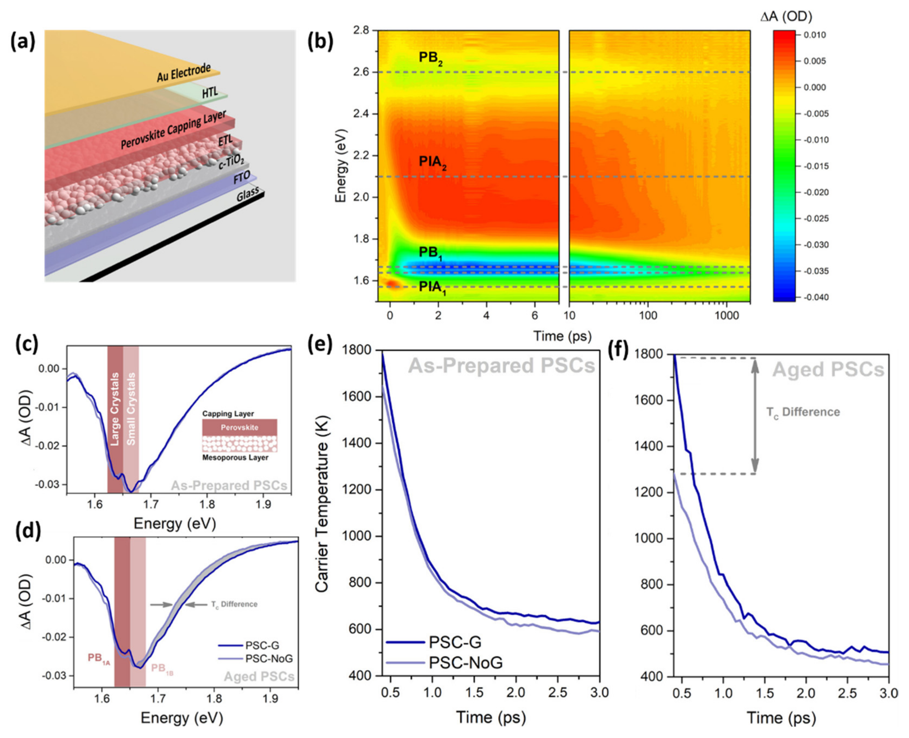
Figure 3.
(a) Pseudo-colour transient absorption plot of clean graphene/MAPbI3 interface at different probe wavelength and with pump wavelength of 820 nm. (b) Differential reflection measured from the clean graphene MAPbI3 heterostructure with 680 nm probe pulse. (c) Normalized differential reflection measured from both dirty- and clean-graphene/MAPbI3 interface. The dashed line is the laser cross-correlation function used for the deconvolution of the rising part of the transient absorption signal. (d) Normalized time resolved photoluminescence spectroscopy measurements performed on pristine MAPbI3 and on clean and dirty graphene/MAPbI3 interfaces. (e) Differential reflection measured from the pristine MAPbI3, the pristine graphene and the clean graphene/MAPbI3 interface. (f) Comparison of the theoretical time-dependent density function calculations and experimental results of charge collection time of the carriers. Data taken from ref. [65]. Copyright American Chemical Society@2018.
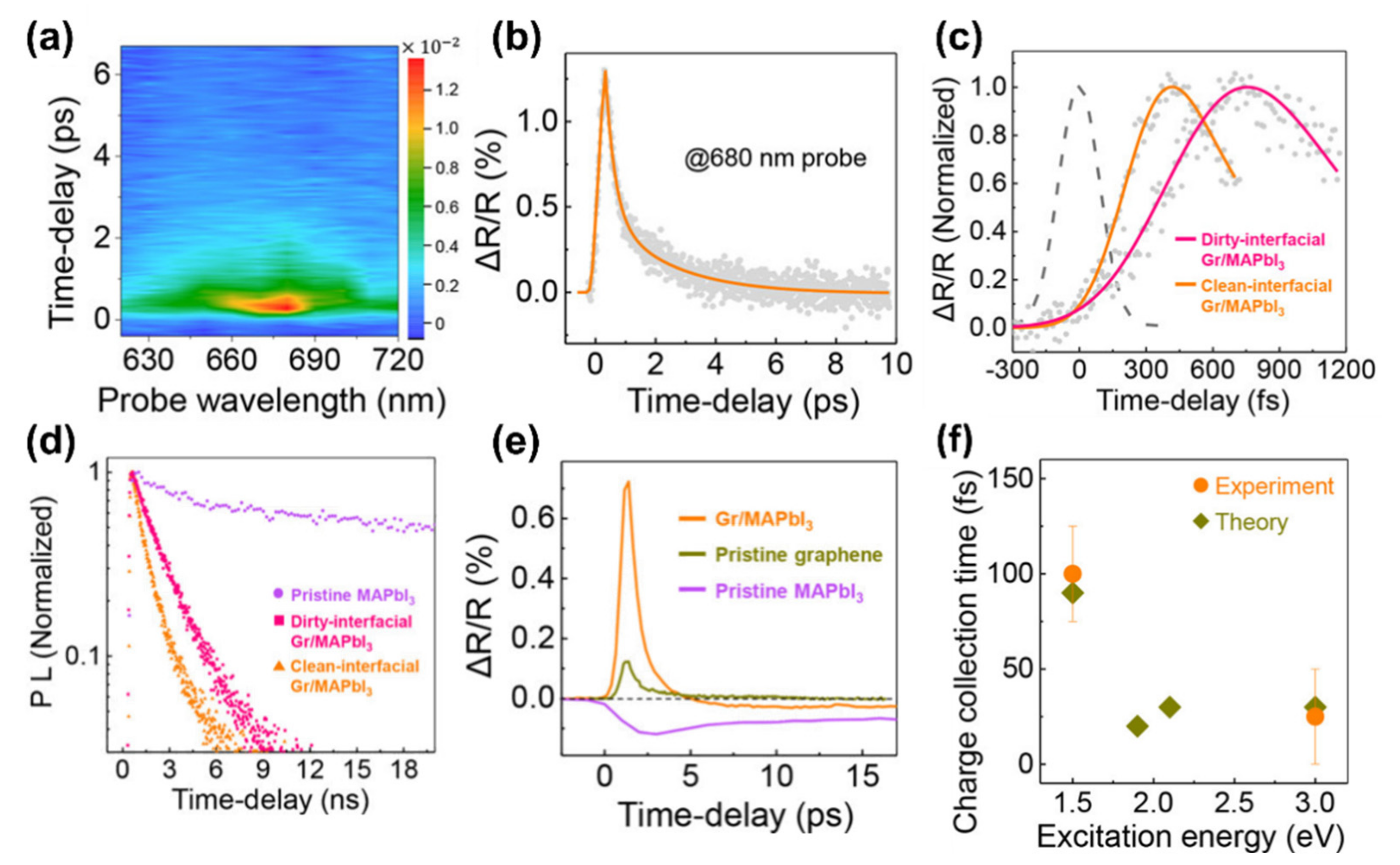
Figure 4.
Schematic representation of the photoinduced hot carriers dynamics at MAPbI3/graphene interface: (a) the hot electrons in MAPbI3 relax to the conduction band minimum (CBM) and then transfer to graphene (pathway 1), (b) the hot electrons in MAPbI3 diffuse to graphene and then relax to the Dirac point (pathway 2), (c) the hot electrons in MAPbI3 follow a zigzag path between MAPbI3 and graphene. (d) Population at graphene of the hot electrons with energies of 2.9 and 3.2 eV above the Fermi level of the MAPbI3/graphene interface as a function of time after optical excitation. Figures adapted from ref. [66]. Copyright American Chemical Society@2021.

Figure 5.
(a) XRD patterns of perovskite films as a function of Cl–GO amounts. SEM images of perovskite films with different amounts of Cl–GO in the precursor solution: (b) pristine 0.0 vol%, (c) 1.0 vol%, (d) 2.0 vol%, (e) 5.0 vol%, and (f) 7.5 vol% Cl-GO. Data taken from ref. [85]. Copyright Springer Science Business Media, LLC, part of Springer Nature@2020.
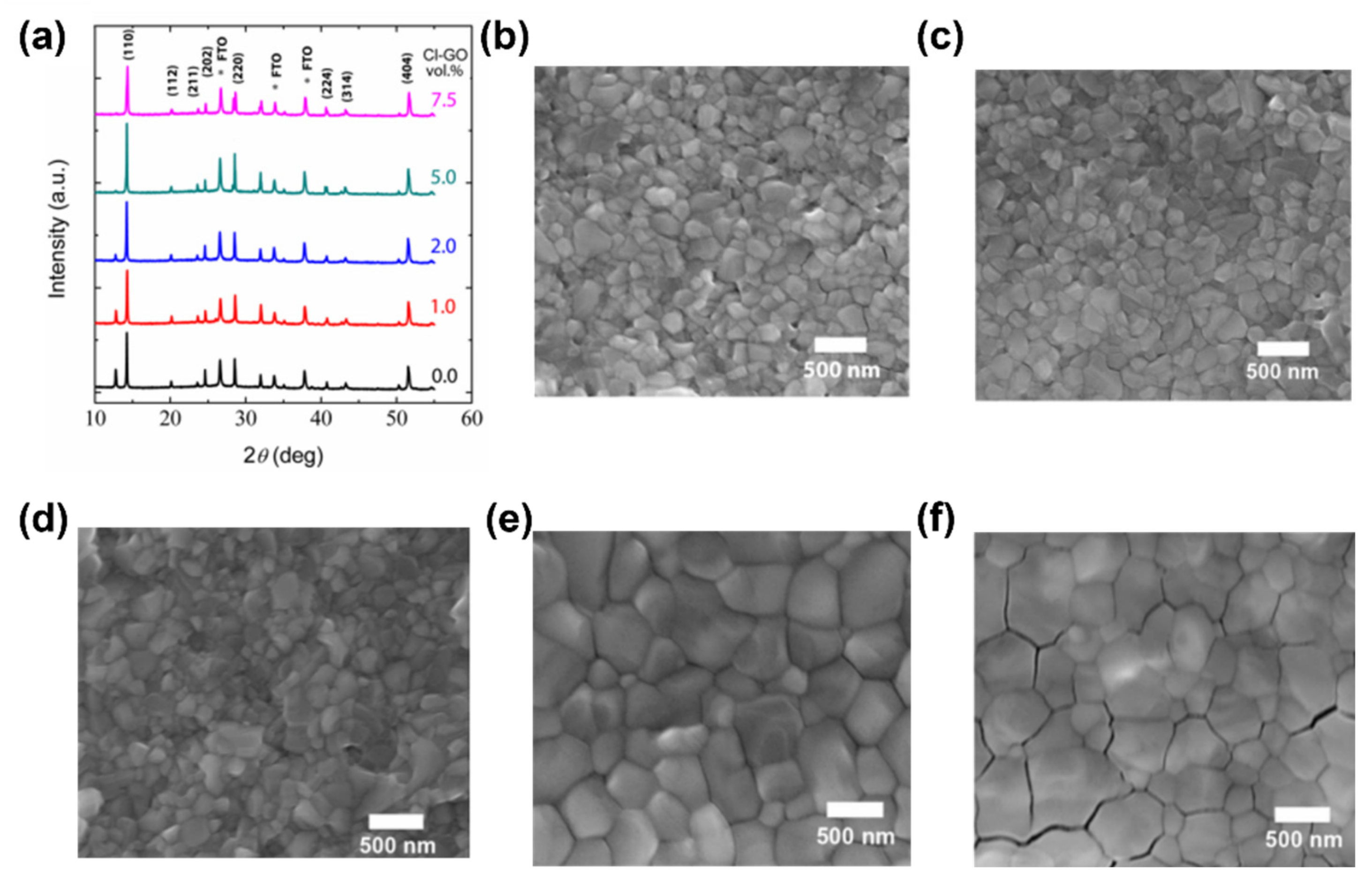
Figure 6.
(a) XRD patterns of MAPbI3 and MAPbI3/WSe2 films; (b) SEM images of MAPbI3 and MAPbI3/WSe2 films; (c) Nyquist plots of MAPbI3 and MAPbI3/WSe2-based PSCs; (d) PL spectra of the MAPbI3 and MAPbI3/WSe2 films with and without hole-transporting layer (HTL); (e) TRPL decay curves of the MAPbI3+HTL and MAPbI3/WSe2+HTL structures; (f) Photostability of non-encapsulated MAPbI3 and MAPbI3/WSe2 based PSC devices under storage in N2 glovebox (illumination of 100 mW cm−2 white light-emitting diode (LED) for 500 h). Data taken from ref. [86]. Copyright American Chemical Society@2021.

Table 1.
Band gap and carrier mobility of some representative 2D materials.
| Material | Band Gap (eV) | Carrier Mobility (cm2V−1s−1) | Ref |
|---|---|---|---|
| Graphene | 0 | ~2 × 10⁵ | [17] |
| MoS2 | 1.2–1.8 | 10–200 | [17] |
| WS2 | 1.3–2.1 | 43–234 | [18,19,20] |
| WSe2 | 1.2–1.7 | 140–500 | [17] |
| SnS2 | 2.18–2.44 | 50–230 | [21,22] |
| TiS2 | 0.02–2.5 | 7.24 | [23,24] |
| Ti2CO2 | 0.91 | ~400 | [25,26] |
| HfCO2 | 1.79 | ~1100 | [25,27] |
| Zr2CO2 | 1.76 | ~600 | [25,27] |
Publisher’s Note: MDPI stays neutral with regard to jurisdictional claims in published maps and institutional affiliations. |
© 2021 by the authors. Licensee MDPI, Basel, Switzerland. This article is an open access article distributed under the terms and conditions of the Creative Commons Attribution (CC BY) license (https://creativecommons.org/licenses/by/4.0/).
Share and Cite
MDPI and ACS Style
Verduci, R.; Agresti, A.; Romano, V.; D’Angelo, G. Interface Engineering for Perovskite Solar Cells Based on 2D-Materials: A Physics Point of View. Materials 2021, 14, 5843. https://doi.org/10.3390/ma14195843
AMA Style
Verduci R, Agresti A, Romano V, D’Angelo G. Interface Engineering for Perovskite Solar Cells Based on 2D-Materials: A Physics Point of View. Materials. 2021; 14(19):5843. https://doi.org/10.3390/ma14195843
Chicago/Turabian StyleVerduci, Rosaria, Antonio Agresti, Valentino Romano, and Giovanna D’Angelo. 2021. "Interface Engineering for Perovskite Solar Cells Based on 2D-Materials: A Physics Point of View" Materials 14, no. 19: 5843. https://doi.org/10.3390/ma14195843
Note that from the first issue of 2016, this journal uses article numbers instead of page numbers. See further details here.