
In Situ Monitoring of Pulsed Laser Annealing of Eu-Doped Oxide Thin Films

 , , , , , ,
Abstract
:1. Introduction
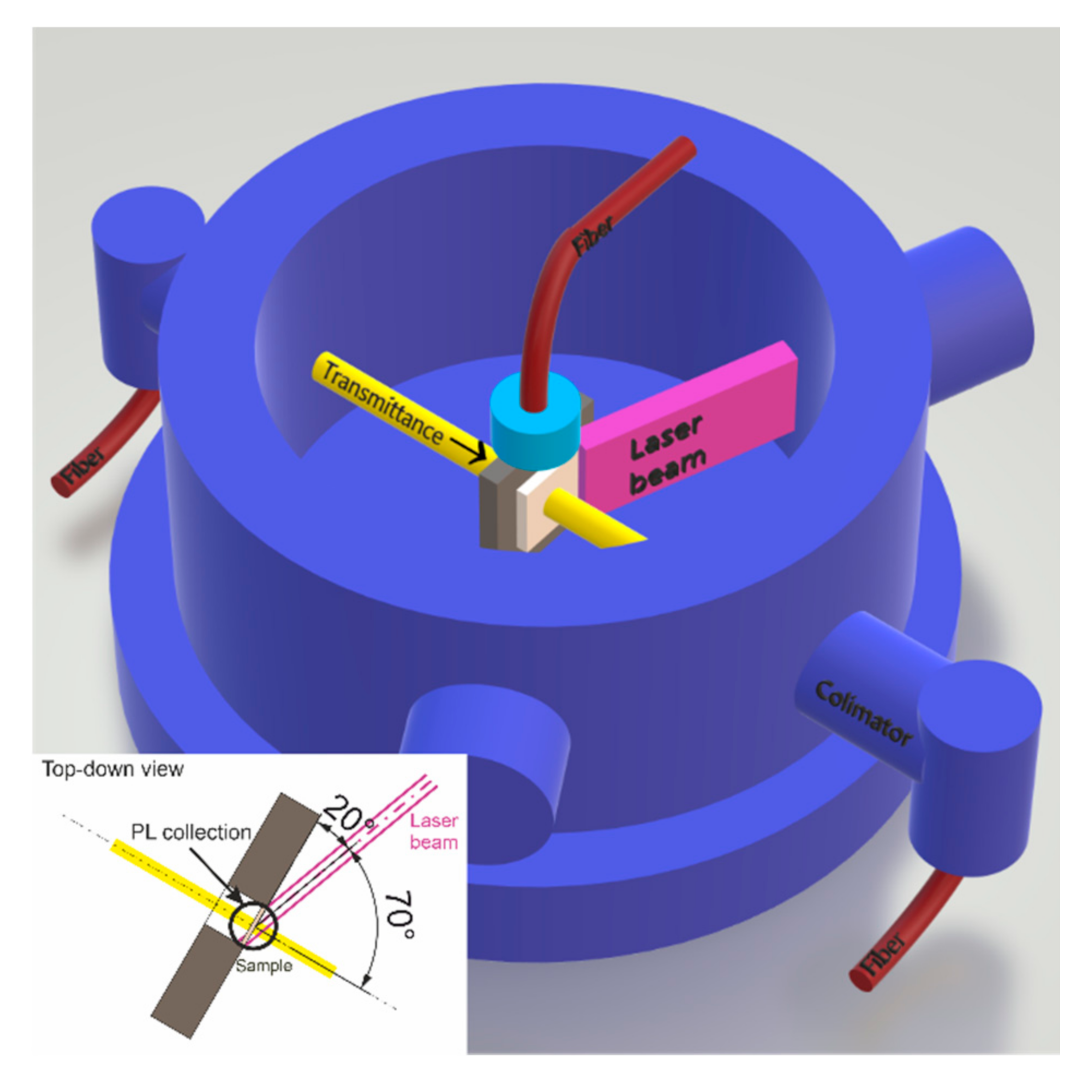
2. Materials and Methods
3. Results and Discussion
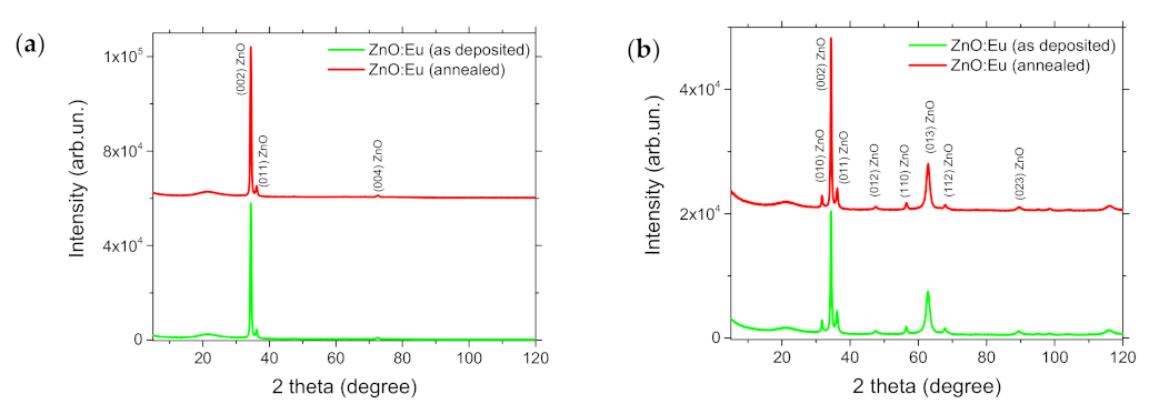
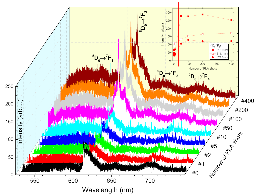
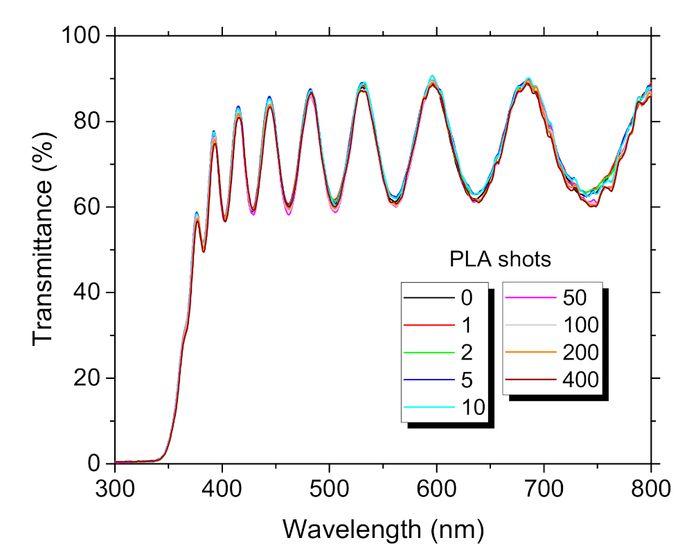
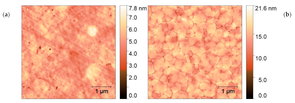
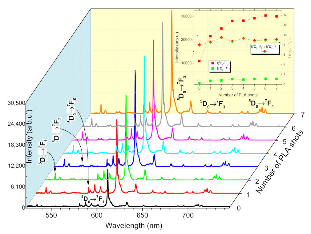
3.1. ZnO:Eu
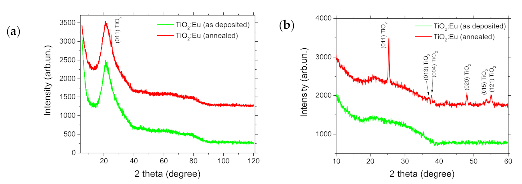
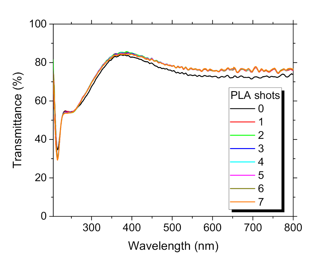
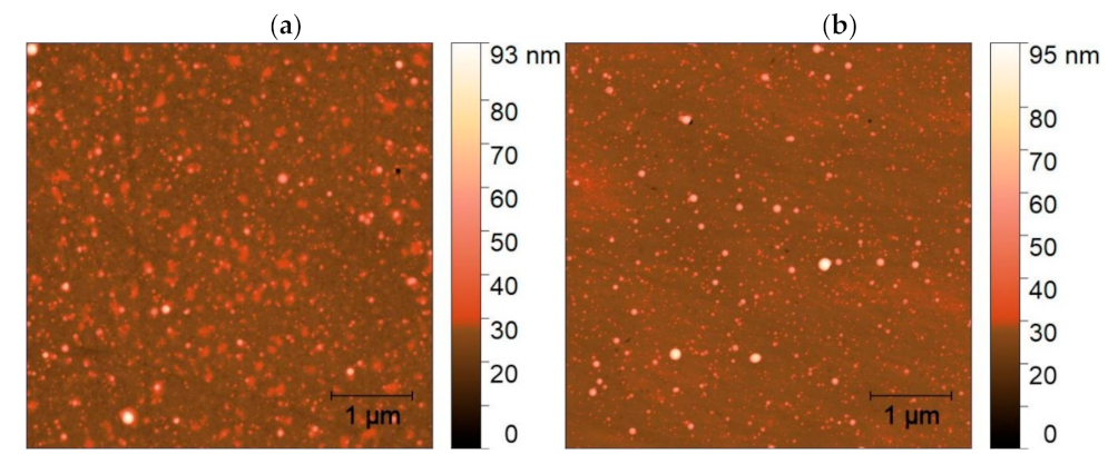
3.2. TiO2:Eu
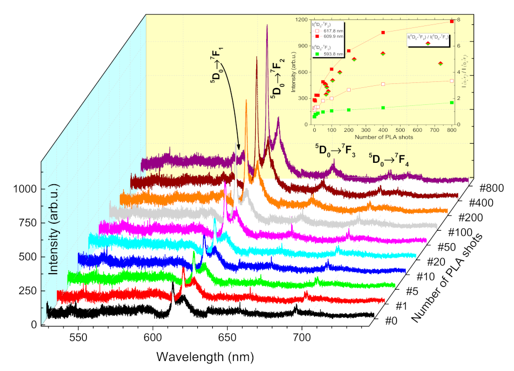
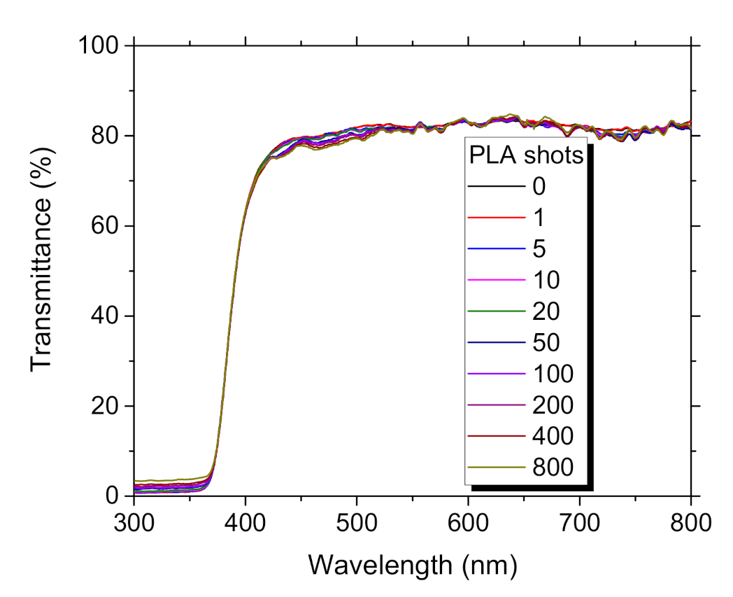
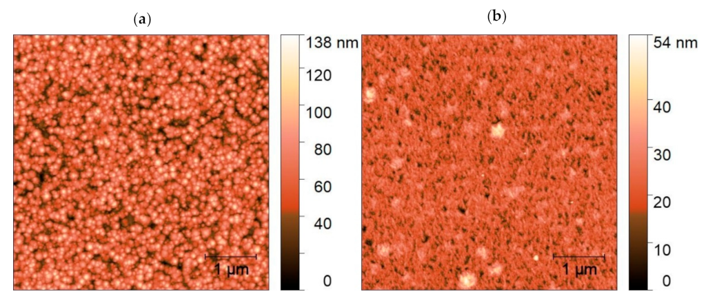
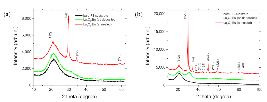
3.3. Lu2O3:Eu
4. Conclusions
Author Contributions
Funding
Institutional Review Board Statement
Informed Consent Statement
Data Availability Statement
Acknowledgments
Conflicts of Interest
References
- Daksh, D.; Agrawal, Y.K. Rare Earth-Doped Zinc Oxide Nanostructures: A Review. Rev. Nanosci. Nanotechnol. 2016, 5, 1–27. [Google Scholar] [CrossRef]
- Gupta, S.K.; Sudarshan, K.; Kadam, R. Optical nanomaterials with focus on rare earth doped oxide: A Review. Mater. Today Commun. 2021, 27, 102277. [Google Scholar] [CrossRef]
- Topping, S.G.; Sarin, V.K. CVD Lu2O3:Eu coatings for advanced scintillators. Int. J. Refract. Met. Hard Mater. 2009, 27, 498–501. [Google Scholar] [CrossRef] [PubMed] [Green Version]
- Nagarkar, V.V.; Topping, S.G.; Miller, S.R.; Singh, B.; Brecher, C.; Sarin, V.K. Characterization of vapor-deposited Lu2O3: Eu3+ scintillator for x-ray imaging applications. In Penetrating Radiation Systems and Applications X; International Society for Optics and Photonics: Bellingham, WA, USA, 2009; Volume 7450, p. 745003. [Google Scholar] [CrossRef]
- Li, G.-R.; Dawa, C.-R.; Lu, X.-H.; Yu, X.-L.; Tong, Y.-X. Use of Additives in the Electrodeposition of Nanostructured Eu3+/ZnO Films for Photoluminescent Devices. Langmuir 2009, 25, 2378–2384. [Google Scholar] [CrossRef] [PubMed]
- Chen, P.; Wang, Z.; Wang, S.; Lyu, M.; Hao, M.; Ghasemi, M.; Xiao, M.; Yun, J.-H.; Bai, Y.; Wang, L. Luminescent europium-doped titania for efficiency and UV-stability enhancement of planar perovskite solar cells. Nano Energy 2020, 69, 104392. [Google Scholar] [CrossRef]
- Ezirmik, K.V. Concentration quenching of photoluminescence in optically transparent Lu2O3:Eu thin films deposited to be used as scintillators. Mater. Res. Express 2021, 8, 016407. [Google Scholar] [CrossRef]
- Zhu, C.; Lv, C.; Wang, C.; Sha, Y.; Li, D.; Ma, X.; Yang, D. Color-tunable electroluminescence from Eu-doped TiO(2)/p(+)-Si heterostructured devices: Engineering of energy transfer. Opt. Express 2015, 23, 2819–2826. [Google Scholar] [CrossRef] [PubMed]
- Murillo, A.G.; Romo, F.D.J.C.; Le Luyer, C.; Ramírez, A.D.J.M.; Hernández, M.G.; Palmerin, J.M. Sol–gel elaboration and structural investigations of Lu2O3:Eu3+ planar waveguides. J. Sol-Gel Sci. Technol. 2009, 50, 359–367. [Google Scholar] [CrossRef]
- Thoř, T.; Rubešová, K.; Jakeš, V.; Cajzl, J.; Nádherný, L.; Mikolášová, D.; Beitlerová, A.; Nikl, M. Europium-doped Lu2O3 phosphors prepared by a sol-gel method. IOP Conf. Series: Mater. Sci. Eng. 2019, 465, 012009. [Google Scholar] [CrossRef]
- Zhang, J.; Qin, Q.; Yu, M.; Zhou, M.; Wang, Y. The photoluminescence, afterglow and up conversion photostimulated luminescence of Eu3+ doped Mg2SnO4 phosphors. J. Lumin. 2012, 132, 23–26. [Google Scholar] [CrossRef]
- Binnemans, K. Interpretation of europium(III) spectra. Co-ord. Chem. Rev. 2015, 295, 1–45. [Google Scholar] [CrossRef] [Green Version]
- Miranda, S.; Peres, M.; Monteiro, T.; Alves, E.; Sun, H.; Geruschke, T.; Vianden, R.; Lorenz, K. Rapid thermal annealing of rare earth implanted ZnO epitaxial layers. Opt. Mater. 2011, 33, 1139–1142. [Google Scholar] [CrossRef]
- Najafi, M.; Haratizadeh, H. The effect of growth conditions and morphology on photoluminescence properties of Eu-doped ZnO nanostructures. Solid State Sci. 2015, 41, 48–51. [Google Scholar] [CrossRef]
- Kaszewski, J.; Kiełbik, P.; Wolska, E.; Witkowski, B.; Wachnicki, Ł; Gajewski, Z.; Godlewski, M.M. Tuning the luminescence of ZnO:Eu nanoparticles for applications in biology and medicine. Opt. Mater. 2018, 80, 77–86. [Google Scholar] [CrossRef]
- Wang, M.; Huang, C.; Huang, Z.; Guo, W.; Huang, J.; He, H.; Wang, H.; Cao, Y.; Liu, Q.; Liang, J. Synthesis and photoluminescence of Eu-doped ZnO microrods prepared by hydrothermal method. Opt. Mater. 2009, 31, 1502–1505. [Google Scholar] [CrossRef]
- Swapna, R.; Srinivasa Reddy, T.; Venkateswarlu, K.; Kumar, M.S. Effect of Post-Annealing on the Properties of Eu Doped ZnO Nano Thin Films. Procedia Mater. Sci. 2015, 10, 723–729. [Google Scholar] [CrossRef] [Green Version]
- Al-Shomar, S.M. Synthesis and characterization of Eu3+ doped TiO2 thin films deposited by spray pyrolysis technique for photocatalytic application. Mater. Res. Express 2021, 8, 026402. [Google Scholar] [CrossRef]
- Akazawa, H.; Shinojima, H. Switching photoluminescence channels between dopant Eu2+ and Eu3+ ions in ZnO thin films by varying the post-annealing conditions. J. Appl. Phys. 2016, 120, 123101. [Google Scholar] [CrossRef]
- Topping, S.G.; Park, C.H.; Rangan, S.K.; Sarin, V.K. Lutetium Oxide Coatings by PVD. MRS Online Proc. Library (OPL) 2007, 1038, 115–120. [Google Scholar] [CrossRef] [Green Version]
- Roy, S.; Topping, S.; Sarin, V. Growth and Characterization of Lu2O3:Eu3+ Thin Films on Single-Crystal Yttria-Doped Zirconia. JOM 2013, 65, 557–561. [Google Scholar] [CrossRef]
- Marton, Z.; Miller, S.R.; Brecher, C.; Kenesei, P.; Moore, M.D.; Woods, R.; Almer, J.D.; Miceli, A.; Nagarkar, V.V. Efficient high-resolution hard X-ray imaging with transparent Lu2O3:Eu scintillator thin films. In Medical Applications of Radiation Detectors V; International Society for Optics and Photonics: Bellingham, WA, USA, 2015; Volume 9594, p. 95940E. [Google Scholar] [CrossRef]
- Márton, Z.; Bhandari, H.B.; Brecher, C.; Miller, S.R.; Singh, B.; Nagarkar, V.V. High efficiency microcolumnar Lu2O3:Eu scintillator thin film for hard X-ray microtomography. J. Physics: Conf. Ser. 2013, 425, 062016. [Google Scholar] [CrossRef] [Green Version]
- Novotny, M.; Vondráček, M.; Marešová, E.; Fitl, P.; Bulíř, J.; Pokorný, P.; Havlová, Š.; Abdellaoui, N.; Pereira, A.; Hubík, P.; et al. Optical and structural properties of ZnO:Eu thin films grown by pulsed laser deposition. Appl. Surf. Sci. 2019, 476, 271–275. [Google Scholar] [CrossRef]
- Martinet, C.; Pillonnet, A.; Lancok, J.; Garapon, C. Optical, structural and fluorescence properties of nanocrystalline cubic or monoclinic Eu:Lu2O3 films prepared by pulsed laser deposition. J. Lumin. 2007, 126, 807–816. [Google Scholar] [CrossRef]
- Le Boulbar, E.; Millon, E.; Boulmer-Leborgne, C.; Cachoncinlle, C.; Hakim, B.; Ntsoenzok, E. Optical properties of rare earth-doped TiO2 anatase and rutile thin films grown by pulsed-laser deposition. Thin Solid Films 2014, 553, 13–16. [Google Scholar] [CrossRef]
- Irimiciuc, S.; More-Chevalier, J.; Chertpalov, S.; Fekete, L.; Novotný, M.; Havlová, Š.; Poupon, M.; Zikmund, T.; Kůsová, K.; Lančok, J. In-situ plasma monitoring by optical emission spectroscopy during pulsed laser deposition of doped Lu2O3. Appl. Phys. A 2021, 127, 1–9. [Google Scholar] [CrossRef]
- Camps, I.; Borlaf, M.; Colomer, M.T.; Moreno, R.; Duta, L.; Nita, C.; del Pino, A.P.; Logofatu, C.; Serna, R.; György, E. Structure-property relationships for Eu doped TiO2 thin films grown by a laser assisted technique from colloidal sols. RSC Adv. 2017, 7, 37643–37653. [Google Scholar] [CrossRef] [Green Version]
- Garcıa-Murillo, A.; Le Luyer, C.; Dujardin, C.; Martin, T.; Garapon, C.; Pédrini, C.; Mugnier, J. Elaboration and scintillation properties of Eu3+-doped Gd2O3 and Lu2O3 sol–gel films. Nucl. Instrum. Methods Phys. Res. Sect. A Accel. Spectromet. Detect. Assoc. Equip. 2002, 486, 181–185. [Google Scholar] [CrossRef]
- Fhoula, M.; Kallel, T.; Messaoud, M.; Dammak, M.; Cavalli, E. Morphological, spectroscopic and photocatalytic properties of Eu3+:TiO2 synthesized by solid-state and hydrothermal-assisted sol-gel processes. Ceram. Int. 2019, 45, 3675–3679. [Google Scholar] [CrossRef]
- Frindell, K.L.; Bartl, M.H.; Popitsch, A.; Stucky, G.D. Sensitized Luminescence of Trivalent Europium by Three-Dimensionally Arranged Anatase Nanocrystals in Mesostructured Titania Thin Films. Angew. Chem. Int. Ed. 2002, 41, 959–962. [Google Scholar] [CrossRef]
- Ramírez, A.D.J.M.; Hernández, M.G.; Murillo, A.G.; Romo, F.D.J.C.; Palmerin, J.M.; Velazquez, D.Y.M.; Jota, M.L.C. Structural and Luminescence Properties of Lu2O3:Eu3+ F127 Tri-Block Copolymer Modified Thin Films Prepared by Sol-Gel Method. Materials 2013, 6, 713–725. [Google Scholar] [CrossRef] [Green Version]
- Chen, P.; X. Ma, X.; Yang, D. ZnO:Eu thin-films: Sol–gel derivation and strong photoluminescence from 5D0→7F0 transition of Eu3+ ions. J. Alloy. Compd. 2007, 431, 317–320. [Google Scholar] [CrossRef]
- Can, N.; Townsend, P.D.; Hole, D.E.; Snelling, H.; Ballesteros, J.M.; Afonso, C.N. Enhancement of luminescence by pulse laser annealing of ion-implanted europium in sapphire and silica. J. Appl. Phys. 1995, 78, 6737–6744. [Google Scholar] [CrossRef] [Green Version]
- Can, N.; Townsend, P.D.; Hole, D.E.; Afonso, C.N. High intensity luminescence from pulsed laser annealed europium implanted sapphire. Appl. Phys. Lett. 1994, 65, 1871–1873. [Google Scholar] [CrossRef] [Green Version]
- Ozerov, I.; Arab, M.; Safarov, V.; Marine, W.; Giorgio, S.; Sentis, M.; Nanai, L. Enhancement of exciton emission from ZnO nanocrystalline films by pulsed laser annealing. Appl. Surf. Sci. 2004, 226, 242–248. [Google Scholar] [CrossRef] [Green Version]
- Havlová, Š.; Novotný, M.; Fitl, P.; More-Chevalier, J.; Remsa, J.; Kiisk, V.; Kodu, M.; Jaaniso, R.; Hruška, P.; Lukáč, F.; et al. Effect of pulsed laser annealing on optical and structural properties of ZnO:Eu thin film. J. Mater. Sci. 2021, 56, 11414–11425. [Google Scholar] [CrossRef]
- Chen, Z.; Jiang, S.; Xin, B.; Guo, R.; Miao, D. Microstructures and luminescent properties of CO2 laser annealed Y2O3:Eu3+ thin films grown on quartz fabric by electron beam evaporation. Text. Res. J. 2018, 88, 1824–1833. [Google Scholar] [CrossRef]
- Jota, M.C.; Murillo, A.G.; Romo, F.C.; Hernández, M.G.; Ramírez, A.D.J.M.; Velumani, S.; Cruz, E.D.L.R.; Kassiba, A. Lu2O3:Eu3+ glass ceramic films: Synthesis, structural and spectroscopic studies. Mater. Res. Bull. 2014, 51, 418–425. [Google Scholar] [CrossRef]
- Xu, M.; Zhang, W.; Dong, N.; Jiang, Y.; Tao, Y.; Yin, M. Preparation and characterization of optical spectroscopy of Lu2O3:Eu nanocrystals. J. Solid State Chem. 2005, 178, 477–482. [Google Scholar] [CrossRef]
- Jurek, K.; Szczesny, R.; Trzcinski, M.; Ciesielski, A.; Borysiuk, J.; Skowronski, L. The Influence of Annealing on the Optical Properties and Microstructure Recrystallization of the TiO2 Layers Produced by Means of the E-BEAM Technique. Materials 2021, 14, 5863. [Google Scholar] [CrossRef] [PubMed]
- Özgür, Ü.; Alivov, Y.I.; Liu, C.; Teke, A.; Reshchikov, M.A.; Doğan, S.; Avrutin, V.; Cho, S.J.; Morkoç, H. A comprehensive review of ZnO materials and devices. J. Appl. Phys. 2005, 98, 041301. [Google Scholar] [CrossRef] [Green Version]
- Zhang, D.; Lin, W.; Lin, Z.; Jia, L.; Zheng, W.; Huang, F. Lu2O3: A promising ultrawide bandgap semiconductor for deep UV photodetector. Appl. Phys. Lett. 2021, 118, 211906. [Google Scholar] [CrossRef]
- Peres, M.; Cruz, A.; Pereira, S.; Correia, M.R.; Soares, M.; Neves, A.; Carmo, M.; Monteiro, T.; Martins, M.; Trindade, T.; et al. Optical studies of ZnO nanocrystals doped with Eu3+ ions. Appl. Phys. A 2007, 88, 129–133. [Google Scholar] [CrossRef]
- Zhang, Y.; Liu, Y.; Wu, L.; Xie, E.; Chen, J. Photoluminescence and ZnO→Eu3+energy transfer in Eu3+-doped ZnO nanospheres. J. Phys. D Appl. Phys. 2009, 42, 085106. [Google Scholar] [CrossRef]
- Ningthoujam, R.; Gajbhiye, N.S.; Ahmed, A.; Umre, S.S.; Sharma, S.J. Re-Dispersible Li+ and Eu3+ Co-Doped Nanocrystalline ZnO: Luminescence and EPR Studies. J. Nanosci. Nanotechnol. 2008, 8, 3059–3062. [Google Scholar] [CrossRef]
- Ishizumi, A.; Kanemitsu, Y. Structural and luminescence properties of Eu-doped ZnO nanorods fabricated by a microemulsion method. Appl. Phys. Lett. 2005, 86, 253106. [Google Scholar] [CrossRef] [Green Version]
- Nedyalkov, N.; Koleva, M.; Nikov, R.; Atanasov, P.; Nakajima, Y.; Takami, A.; Shibata, A.; Terakawa, M. Laser nanostructuring of ZnO thin films. Appl. Surf. Sci. 2016, 374, 172–176. [Google Scholar] [CrossRef]
- Chen, X.; Luo, W. Optical Spectroscopy of Rare Earth Ion-Doped TiO2 Nanophosphors. J. Nanosci. Nanotechnol. 2010, 10, 1482–1494. [Google Scholar] [CrossRef] [PubMed]
- Yin, J.; Xiang, L.; Zhao, X. Monodisperse spherical mesoporous Eu-doped TiO2 phosphor particles and the luminescence properties. Appl. Phys. Lett. 2007, 90, 113112. [Google Scholar] [CrossRef]
- Makuła, P.; Pacia, M.; Macyk, W. How To Correctly Determine the Band Gap Energy of Modified Semiconductor Photocatalysts Based on UV–Vis Spectra. J. Phys. Chem. Lett. 2018, 9, 6814–6817. [Google Scholar] [CrossRef] [PubMed] [Green Version]
- Skowronski, L.; Zdunek, K.; Nowakowska-Langier, K.; Chodun, R.; Trzcinski, M.; Kobierski, M.; Kustra, M.; Wachowiak, A.; Wachowiak, W.; Hiller, T.; et al. Characterization of microstructural, mechanical and optical properties of TiO2 layers deposited by GIMS and PMS methods. Surf. Coat. Technol. 2015, 282, 16–23. [Google Scholar] [CrossRef]
- Wei, H.; Ma, X.; Gu, L.; Li, J.; Si, W.; Ou, G.; Yu, W.; Zhao, C.; Li, J.; Song, M.; et al. Aerodynamic levitated laser annealing method to defective titanium dioxide with enhanced photocatalytic performance. Nano Res. 2016, 9, 3839–3847. [Google Scholar] [CrossRef]
- Pan, H.; Ko, S.H.; Misra, N.; Grigoropoulos, C.P. Laser annealed composite titanium dioxide electrodes for dye-sensitized solar cells on glass and plastics. Appl. Phys. Lett. 2009, 94, 071117. [Google Scholar] [CrossRef] [Green Version]
- Serga, V.; Burve, R.; Krumina, A.; Pankratova, V.; Popov, A.I.; Pankratov, V. Study of phase composition, photocatalytic activity, and photoluminescence of TiO2 with Eu additive produced by the extraction-pyrolytic method. J. Mater. Res. Technol. 2021, 13, 2350–2360. [Google Scholar] [CrossRef]
- Jia, G.; Zheng, Y.; Liu, K.; Song, Y.; You, H.; Zhang, H. Facile Surfactant- and Template-Free Synthesis and Luminescent Properties of One-Dimensional Lu2O3:Eu3+ Phosphors. J. Phys. Chem. C 2009, 113, 153–158. [Google Scholar] [CrossRef]
- Zych, E.; Trojan-Piegza, J.; Kępiński, L. Homogeneously precipitated Lu2O3:Eu nanocrystalline phosphor for X-ray detection. Sens. Actuat. B Chem. 2005, 109, 112–118. [Google Scholar] [CrossRef]
- Pedroso, C.C.S.; de Carvalho, J.M.; Rodrigues, L.C.V.; Hölsä, J.; Brito, H. Rapid and Energy-Saving Microwave-Assisted Solid-State Synthesis of Pr3+-, Eu3+-, or Tb3+-Doped Lu2O3 Persistent Luminescence Materials. ACS Appl. Mater. Interfaces 2016, 8, 19593–19604. [Google Scholar] [CrossRef] [PubMed]
- Wiktorczyk, T. Optical properties of electron beam deposited lutetium oxide thin films. Opt. Applicata 2001, 31, 83–92. [Google Scholar]
- Strek, W.; Zych, E.; Hreniak, D. Size effects on optical properties of Lu2O3:Eu3+ nanocrystallites. J. Alloy. Compd. 2002, 344, 332–336. [Google Scholar] [CrossRef]


| Material | Fluence PLD (J⋅cm−2) | O2 Pressure (Pa) | Deposition Time (min) | Thickness (nm) | Fluence PLA (J⋅cm−2) |
|---|---|---|---|---|---|
| ZnO:Eu (1% at. Eu) | 5 | 15 | 8.3 | 840–1000 | 175 |
| TiO2:Eu (1% at. Eu) | 9 | 1 | 25 | 800 | 175 |
| Lu2O3:Eu (3% at. Eu) | 5 | 2.5 | 20 | 110-150 | 150 |
| Material | Eu3+ (5D0→7F2) PL Emission Enhancement | Band Gap Eg (eV) | Roughness S a S q (nm) | ||
|---|---|---|---|---|---|
| PLA | As Deposited | PLA | As Deposited | PLA | |
| ZnO:Eu | 4.1× | 3.28 | 3.25 | 14.6 18.1 | 3.5 4.6 |
| TiO2:Eu | 5× | 3.24 | 3.23 | 0.5 0.6 | 1.4 1.8 |
| Lu2O3:Eu | 2.8× | 5.47 | 5.51 | 2.0 3.8 | 1.5 3.7 |
Publisher’s Note: MDPI stays neutral with regard to jurisdictional claims in published maps and institutional affiliations. |
© 2021 by the authors. Licensee MDPI, Basel, Switzerland. This article is an open access article distributed under the terms and conditions of the Creative Commons Attribution (CC BY) license (https://creativecommons.org/licenses/by/4.0/).
Share and Cite
Novotný, M.; Remsa, J.; Havlová, Š.; More-Chevalier, J.; Irimiciuc, S.A.; Chertopalov, S.; Písařík, P.; Volfová, L.; Fitl, P.; Kmječ, T.; et al. In Situ Monitoring of Pulsed Laser Annealing of Eu-Doped Oxide Thin Films. Materials 2021, 14, 7576. https://doi.org/10.3390/ma14247576
Novotný M, Remsa J, Havlová Š, More-Chevalier J, Irimiciuc SA, Chertopalov S, Písařík P, Volfová L, Fitl P, Kmječ T, et al. In Situ Monitoring of Pulsed Laser Annealing of Eu-Doped Oxide Thin Films. Materials. 2021; 14(24):7576. https://doi.org/10.3390/ma14247576
Chicago/Turabian StyleNovotný, Michal, Jan Remsa, Šárka Havlová, Joris More-Chevalier, Stefan Andrei Irimiciuc, Sergii Chertopalov, Petr Písařík, Lenka Volfová, Přemysl Fitl, Tomáš Kmječ, and et al. 2021. "In Situ Monitoring of Pulsed Laser Annealing of Eu-Doped Oxide Thin Films" Materials 14, no. 24: 7576. https://doi.org/10.3390/ma14247576