
Effect of Twinning on Angle-Resolved Photoemission Spectroscopy Analysis of Ni49.7Mn29.1Ga21.2(100) Heusler Alloy

 , , and
Abstract
:1. Introduction
2. Materials and Methods
3. Results
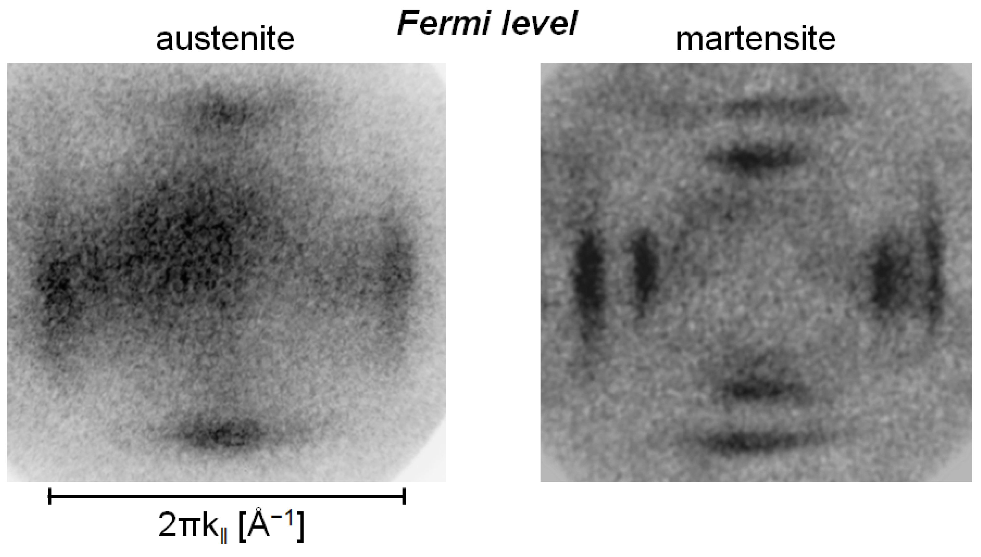
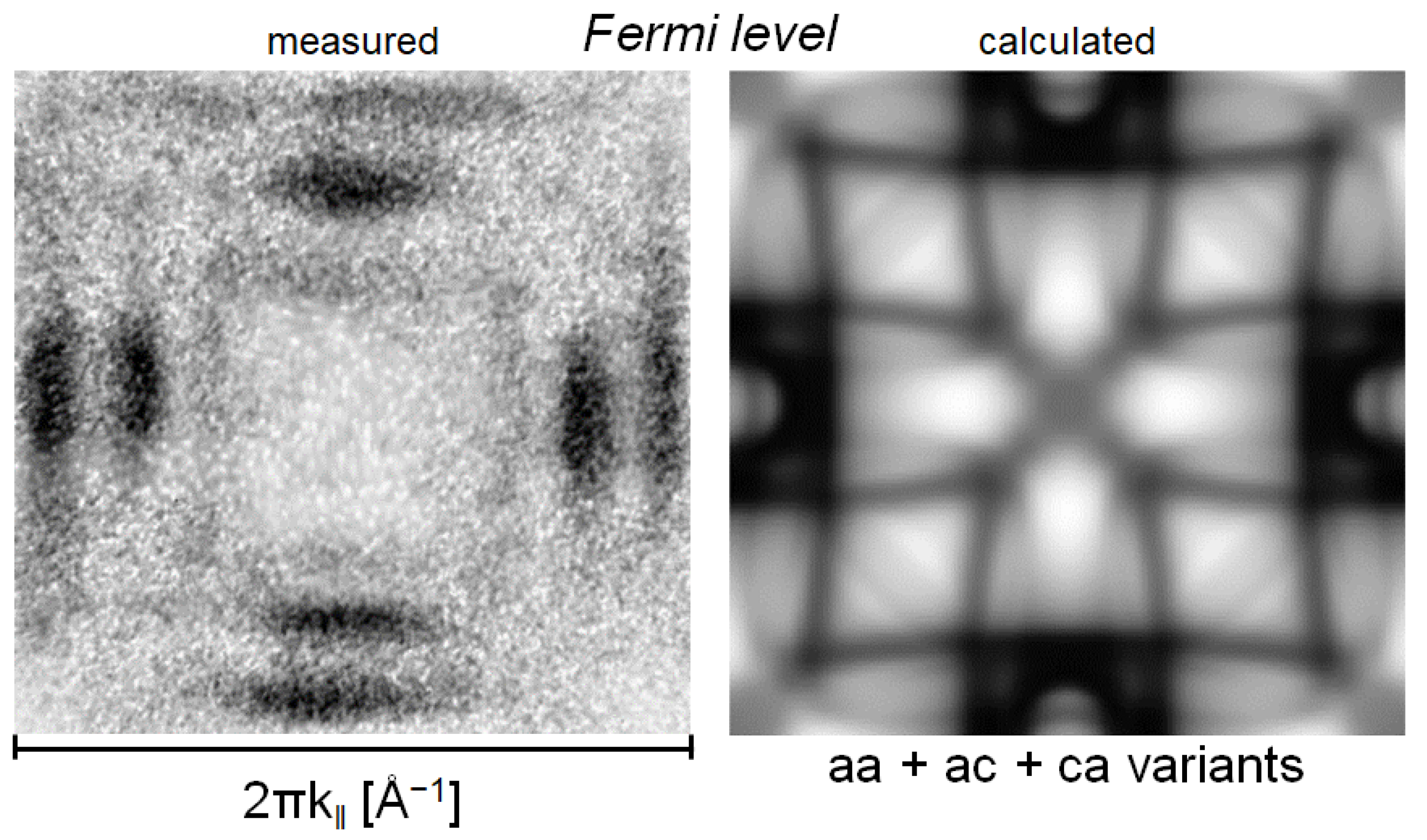
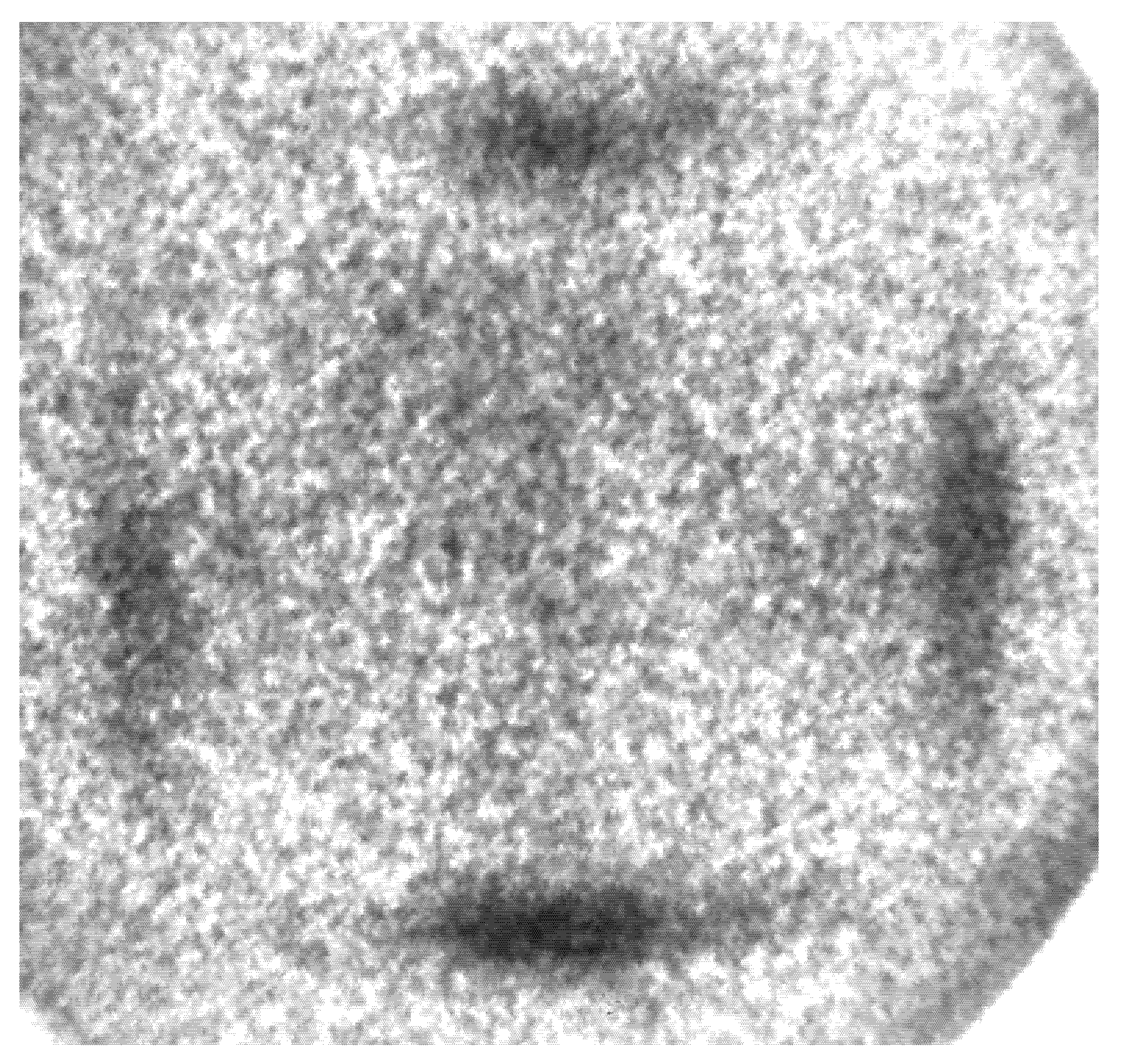
3.1. Experiment
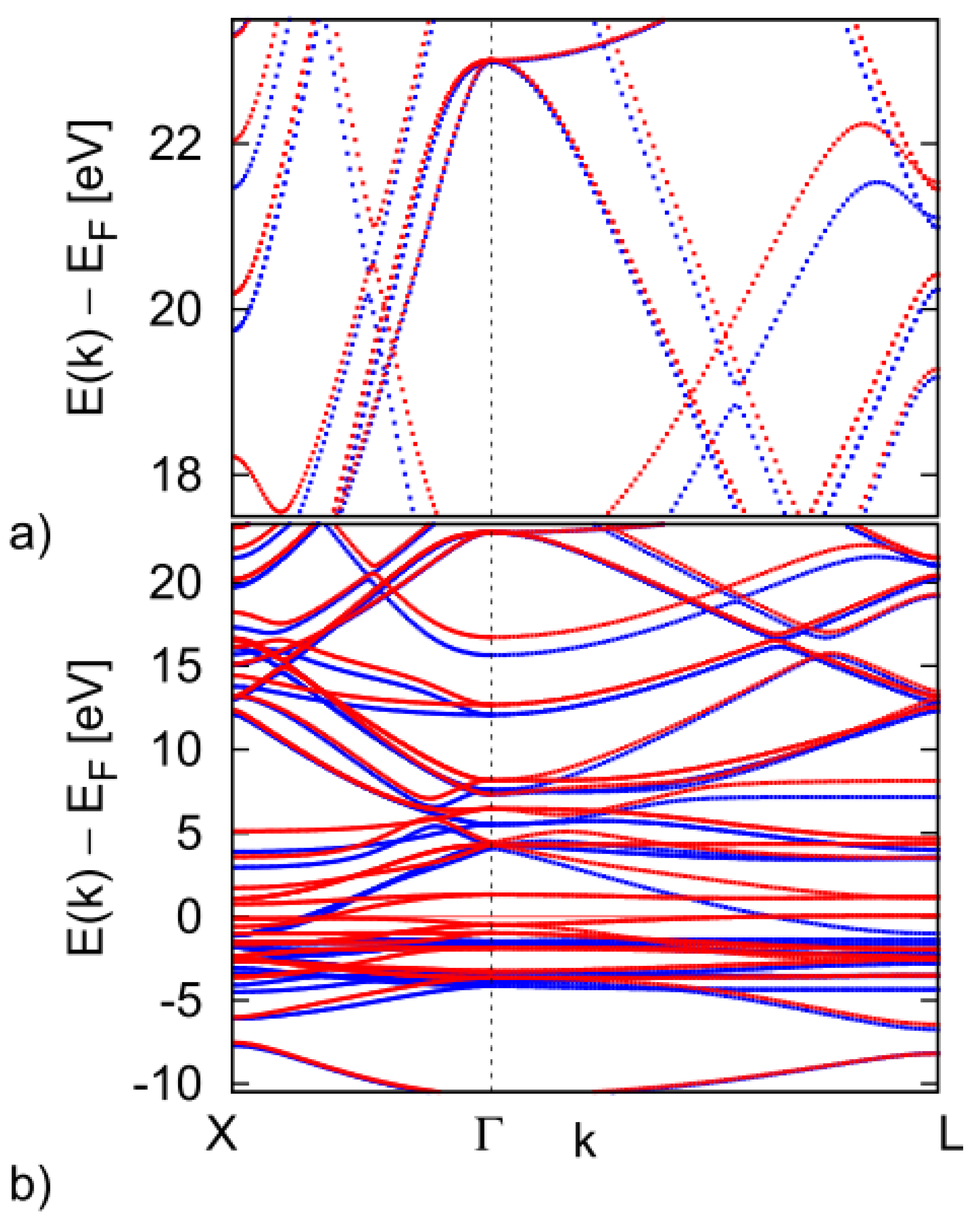
3.2. Theory
4. Discussion
5. Conclusions
Author Contributions
Funding
Institutional Review Board Statement
Informed Consent Statement
Data Availability Statement
Acknowledgments
Conflicts of Interest
References
- Jungwirth, T.; Marti, X.; Wadley, P.; Wunderlich, J. Antiferromagnetic spintronics. Nat. Nanotechnol. 2016, 11, 231–241. [Google Scholar] [CrossRef]
- Nayak, A.K.; Kumar, V.; Ma, T.; Werner, P.; Pippel, E.; Sahoo, R.; Damay, F.; Rößler, U.K.; Felser, C.; Parkin, S.S.P. Magnetic antiskyrmions above room temperature in tetragonal Heusler materials. Nature 2017, 548, 561–566. [Google Scholar] [CrossRef]
- Webster, P.J.; Ziebeck, K.R.A.; Town, S.L.; Peak, M.S. Magnetic order and phase transformation in Ni2MnGa. Philos. Mag. B 1984, 49, 295–310. [Google Scholar] [CrossRef]
- Sozinov, A.; Likhachev, A.A.; Lanska, N.; Ullakko, K. Giant magnetic-field-induced strain in NiMnGa seven-layered martensitic phase. Appl. Phys. Lett. 2002, 80, 1746–1748. [Google Scholar] [CrossRef]
- Niemann, R.; Rößler, U.K.; Gruner, M.E.; Heczko, O.; Schultz, L.; Fähler, S. The Role of Adaptive Martensite in Magnetic Shape Memory Alloys. Adv. Eng. Mater. 2012, 14, 562–581. [Google Scholar] [CrossRef]
- Gregg, J.F.; Allen, W.; Ounadjela, K.; Viret, M.; Hehn, M.; Thompson, S.M.; Coey, J.M.D. Giant Magnetoresistive Effects in a Single Element Magnetic Thin Film. Phys. Rev. Lett. 1996, 77, 1580–1583. [Google Scholar] [CrossRef] [PubMed]
- Thomas, M.; Heczko, O.; Buschbeck, J.; Rößler, U.K.; Mccord, J.; Scheerbaum, N.; Schultz, L.; Fähler, S. Magnetically induced reorientation of martensite variants in constrained epitaxial Ni–Mn–Ga films grown on MgO(001). New J. Phys. 2008, 10, 023040. [Google Scholar] [CrossRef]
- Dunand, D.C.; Müllner, P. Size Effects on Magnetic Actuation in Ni-Mn-Ga Shape-Memory Alloys. Adv. Mater. 2010, 23, 216–232. [Google Scholar] [CrossRef]
- Entel, P.; Buchelnikov, V.D.; Gruner, M.E.; Hucht, A.; Khovailo, V.V.; Nayak, S.K.; Zayak, A.T. Shape Memory Alloys: A Summary of Recent Achievements. Mater. Sci. Forum 2008, 583, 21–41. [Google Scholar] [CrossRef]
- Lee, Y.; Rhee, J.Y.; Harmon, B.N. Generalized susceptibility of the magnetic shape-memory alloy Ni2MnGa. Phys. Rev. B 2002, 66, 054424. [Google Scholar] [CrossRef]
- Polyak, Y.; Drchal, V.; Kudrnovský, J.; Heczko, O.; Honolka, J.; Cháb, V.; Kopeček, J.; Lančok, J. Band mapping of the weakly off-stoichiometric Heusler alloy Ni49.7Mn29.1Ga21.2 in the austenitic phase. Phys. Rev. B 2015, 91, 165115. [Google Scholar] [CrossRef]
- Heczko, O.; Drchal, V.; Cichoň, S.; Fekete, L.; Kudrnovský, J.; Kratochvílová, I.; Lančok, J.; Cháb, V. Electronic structure in the twinned 10M martensite phase of the Ni49.7Mn29.1Ga21.2 Heusler alloy: Experiment and theory. Phys. Rev. B 2018, 98, 184407. [Google Scholar] [CrossRef]
- Turek, I.; Drchal, V.; Kudrnovský, J.; Šob, M.; Weinberger, P. Electronic Structure of Disordered Alloys, Surfaces and Interfaces; Kluwer Academic Publishers: Boston, MA, USA, 1997. [Google Scholar]
- Bhattacharya, K. Microstructure of Martensite: Why It Forms and How It Gives Rise to the Shape-Memory Effect? Oxford University Press: Oxford, UK, 2012. [Google Scholar]
- Heczko, O.; Straka, L.; Seiner, H. Different microstructures of mobile twin boundaries in 10 M modulated Ni–Mn–Ga martensite. Acta Mater. 2013, 61, 622–631. [Google Scholar] [CrossRef]
- Horáková, K.; Cháb, V.; Heczko, O.; Drchal, V.; Fekete, L.; Honolka, J.; Kopeček, J.; Kudrnovský, J.; Polyak, Y.; Sajdl, P.; et al. Surface analysis of the Heusler Ni49.7Mn29.1Ga21.2 Alloy: The composition, phase transition, and twinned microstructure of martensite. J. Appl. Phys. 2016, 120, 113905. [Google Scholar] [CrossRef]
- Bungaro, C.; Rabe, K.M.; Corso, A.D. First-principles study of lattice instabilities in ferromagnetic Ni2MnGa. Phys. Rev. B 2003, 68, 134104. [Google Scholar] [CrossRef] [Green Version]
- Zeng, M.; Cai, M.-Q.; Or, S.W.; Chan, H.L.W. Anisotropy of the electrical transport properties in a Ni2MnGa single crystal: Experiment and theory. J. Appl. Phys. 2010, 107, 083713. [Google Scholar] [CrossRef] [Green Version]
- Adawi, I. Theory of the Surface Photoelectric Effect for One and Two Photons. Phys. Rev. 1964, 134, A788. [Google Scholar] [CrossRef]
- Krasovskii, E.E.; Strocov, V.N.; Barrett, N.; Berger, H.; Schattke, W.; Claessen, R. Band mapping in the one-step photoemission theory: Multi-Bloch-wave structure of final states and interference effects. Phys. Rev. B 2007, 75, 045432. [Google Scholar] [CrossRef] [Green Version]
- Kresse, G.; Joubert, D. From ultrasoft pseudopotentials to the projector augmented-wave method. Phys. Rev. B 1999, 59, 1758–1775. [Google Scholar] [CrossRef]
- Ridzel, O.Y.; Astašauskas, V.; Werner, W.S.M. Low energy (1–100 eV) electron inelastic mean free path (IMFP) values determined from analysis of secondary electron yields (SEY) in the incident energy range of 0.1–10 keV. J. Electron Spectrosc. Relat. Phenom. 2020, 241, 146824. [Google Scholar] [CrossRef]
- Nguyen-Truong, H.T. Low-energy electron inelastic mean free path in materials. Appl. Phys. Lett. 2016, 108, 172901. [Google Scholar] [CrossRef]
- Powell, C.J. Practical guide for inelastic mean free paths, effective attenuation lengths, mean escape depths, and information depths in X-ray photoelectron spectroscopy. J. Vac. Sci. Technol. A 2020, 38, 023209. [Google Scholar] [CrossRef]
- Straka, L.; Heczko, O.; Seiner, H.; Lanska, N.; Drahokoupil, J.; Soroka, A.; Fähler, S.; Hänninen, H.; Sozinov, A. Highly mobile twinned interface in 10M modulated Ni–Mn–Ga martensite: Analysis beyond the tetragonal approximation of lattice. Acta Mater. 2011, 59, 7450–7463. [Google Scholar] [CrossRef]
- Straka, L.; Heczko, O.; Hänninen, H. Activation of magnetic shape memory effect in Ni–Mn–Ga alloys by mechanical and magnetic treatment. Acta Mater. 2008, 56, 5492–5499. [Google Scholar] [CrossRef]
- Heczko, O. Magnetic shape memory effect and highly mobile twin boundaries. Mater. Sci. Technol. 2014, 30, 1559–1578. [Google Scholar] [CrossRef]
- Pons, J.; Chernenko, V.; Santamarta, R.; Cesari, E. Crystal structure of martensitic phases in Ni–Mn–Ga shape memory alloys. Acta Mater. 2000, 48, 3027–3038. [Google Scholar] [CrossRef]
- Kaufmann, S.; Rößler, U.K.; Heczko, O.; Wuttig, M.; Buschbeck, J.; Schultz, L.; Fähler, S. Adaptive Modulations of Martensites. Phys. Rev. Lett. 2010, 104, 145702. [Google Scholar] [CrossRef] [Green Version]
- James, R.; Hane, K. Martensitic transformations and shape-memory materials. Acta Mater. 2000, 48, 197–222. [Google Scholar] [CrossRef]
- Zelený, M.; Straka, L.; Sozinov, A.; Heczko, O. Transformation Paths from Cubic to Low-Symmetry Structures in Heusler Ni2MnGa Compound. Sci. Rep. 2018, 8, 1–8. [Google Scholar] [CrossRef] [Green Version]
- Zelený, M.; Straka, L.; Sozinov, A.; Heczko, O. Ab initio prediction of stable nanotwin double layers and 4O structure in Ni2MnGa. Phys. Rev. B 2016, 94, 224108. [Google Scholar] [CrossRef] [Green Version]
- Ge, Y.; Zárubová, N.; Heczko, O.; Hannula, S.-P. Stress-induced transition from modulated 14M to non-modulated martensite in Ni–Mn–Ga alloy. Acta Mater. 2015, 90, 151–160. [Google Scholar] [CrossRef]
- Wende, H.; Freeland, J.W.; Chakarian, V.; Idzerda, Y.U.; Lemke, L.; Baberschke, K. Probing local magnetic disorder by investigating spin dependent photoelectron scattering. J. Appl. Phys. 1998, 83, 7028–7030. [Google Scholar] [CrossRef]
- Schwabe, S.; Niemann, R.; Backen, A.; Wolf, D.; Damm, C.; Walter, T.; Seiner, H.; Heczko, O.; Nielsch, K.; Fähler, S. Building Hierarchical Martensite. Adv. Funct. Mater. 2020, 31, 2005715. [Google Scholar] [CrossRef]


Publisher’s Note: MDPI stays neutral with regard to jurisdictional claims in published maps and institutional affiliations. |
© 2022 by the authors. Licensee MDPI, Basel, Switzerland. This article is an open access article distributed under the terms and conditions of the Creative Commons Attribution (CC BY) license (https://creativecommons.org/licenses/by/4.0/).
Share and Cite
Cháb, V.; Drchal, V.; Máca, F.; Kudrnovský, J.; Cichoň, S.; Lančok, J.; Heczko, O. Effect of Twinning on Angle-Resolved Photoemission Spectroscopy Analysis of Ni49.7Mn29.1Ga21.2(100) Heusler Alloy. Materials 2022, 15, 717. https://doi.org/10.3390/ma15030717
Cháb V, Drchal V, Máca F, Kudrnovský J, Cichoň S, Lančok J, Heczko O. Effect of Twinning on Angle-Resolved Photoemission Spectroscopy Analysis of Ni49.7Mn29.1Ga21.2(100) Heusler Alloy. Materials. 2022; 15(3):717. https://doi.org/10.3390/ma15030717
Chicago/Turabian StyleCháb, Vladimír, Václav Drchal, František Máca, Josef Kudrnovský, Stanislav Cichoň, Ján Lančok, and Oleg Heczko. 2022. "Effect of Twinning on Angle-Resolved Photoemission Spectroscopy Analysis of Ni49.7Mn29.1Ga21.2(100) Heusler Alloy" Materials 15, no. 3: 717. https://doi.org/10.3390/ma15030717