
Graphene as a Transparent Conductive Electrode in GaN-Based LEDs


Werkstoffe der Elektrotechnik and CENIDE, Universität Duisburg-Essen, 47057 Duisburg, Germany
*
Authors to whom correspondence should be addressed.
Materials 2022, 15(6), 2203; https://doi.org/10.3390/ma15062203
Submission received: 31 January 2022
/
Revised: 23 February 2022
/
Accepted: 26 February 2022
/
Published: 16 March 2022
(This article belongs to the Special Issue Optoelectronic Devices: 2021)
Abstract
:Graphene combines high conductivity (sheet resistance down to a few hundred Ω/sq and even less) with high transparency (>90%) and thus exhibits a huge application potential as a transparent conductive electrode in gallium nitride (GaN)-based light-emitting diodes (LEDs), being an economical alternative to common indium-based solutions. Here, we present an overview of the state-of-the-art graphene-based transparent conductive electrodes in GaN-based LEDs. The focus is placed on the manufacturing progress and the resulting properties of the fabricated devices. Transferred as well as directly grown graphene layers are considered. We discuss the impact of graphene-based transparent conductive electrodes on current spreading and contact resistance, and reveal future challenges and perspectives on the use of graphene in GaN-based LEDs.
1. Introduction
GaN-based light-emitting diodes (LEDs) have been intensively studied for applications in the visible and ultraviolet (UV) spectral range [1,2,3,4]. GaN-based visible light LEDs can be used for general illumination, traffic signals, automobile headlights, and backlight units for liquid crystal displays [5], while GaN-based UV LEDs could be applied in germicidal instrumentation, biological agent identification, chemical sensing, fluorescence excitation, water disinfection and optical data storage [6,7].
Since the commonly used p-type cladding layers in GaN-based LEDs, such as Mg-doped GaN or AlGaN, have deep acceptors with an activation energy of, e.g., around 170 meV in GaN [8] or around 400 meV in Al0.7Ga0.3N [9], the p-cladding layer is not sufficiently conductive [2,10]. As a consequence, current crowding near the p-electrode edges occurs, which could severely deteriorate the stability and reliability of the LED devices [11,12,13,14]. For a more-homogeneous distribution of current, a transparent current spreading layer (TCSL) with low electrical sheet resistance and high optical transparency is essential [15]. In the early stage of GaN-based LED development, the commonly used p-contact material was Ni/Au. To overcome the current crowing problem, scientists attempted to directly use Ni/Au as a transparent conductive electrode and improved the transparency of thin Ni/Au films from around 50% to over 83% in the 400–750 nm spectra region by rapid thermal annealing (RTA) [16]. In the following, studies started to use transparent conductive oxides, such as indium tin oxide (ITO), as TCSL. ITO has both high conductivity and a high transparency of over 85% in the range of 400–600 nm [17,18]. However, as a commercial TCSL the cost increase of ITO due to the low abundance of indium on Earth (around 0.05 ppm) and its low recycling rate (below 10%) is detrimental [19]. Moreover, the intrinsic transmission loss of ITO below 400 nm [20,21] restricted its application in UV-LEDs, and the low thermal conductivity of 11~12 W/m·K of ITO [22] could lead to a high local temperature, potentially degrading the performance of high power GaN-LEDs [23]. Additionally, due to its mechanical brittleness ITO is not suitable for the use in flexible devices [24].
Graphene, defined as a two-dimensional (2D) carbon material consisting of a hexagonal array of sp2-hybridized carbon atoms with a single-atom-thickness, can exhibit a high transparency of >91% in a wide range from 200 nm to 1000 nm [25], a low sheet resistance () of ~250 Ω/sq [25] and a high thermal conductivity of ~2000–4000 W/m·K [26,27,28] that is several hundred times higher than that of ITO. Low-cost fabrication approaches [25,29,30] has made graphene already commercially available [31,32]. Based on these advantages, graphene is considered as a promising candidate for replacing ITO as TCSL in GaN-based LEDs, especially in the UV range. However, the up-to-date contact resistance between graphene and p-GaN is in the order of Ωcm2 [33,34,35], which could originate from the large work function mismatch between graphene of 4.2–4.5 eV [36,37,38] and p-type doped GaN (p-GaN) of ~7.5 eV [39]. This might inhibit the hole injection efficiency and could result in a higher operating voltage.
In the second decade of the 21st century, GaN-based LEDs with graphene as TCSL have been intensively studied. Different aspects of this research are reviewed in this work. The main efforts of these studies focused on the reduction of the contact resistance, and in keeping the low sheet resistance and high transparency of graphene-based TCSL after integration into GaN-based LEDs. In this review, the numerous efforts for integration of graphene-based TCSL in GaN-based LEDs with single- (SQW) or multi-quantum wells (MQW) are summarized. In Section 2, the improvement of properties of graphene-based TCSLs through varying the fabrication methods (Section 2.1) or by realizing graphene hybrid structures (Section 2.2) are described. The fabrication of graphene films includes both transfer (Section 2.1.1) and direct growth (Section 2.1.2) on GaN-based LEDs. Hybrid graphene structure consisting of graphene networked with ITO nanodots (Section 2.2.1), with metal interlayer, nanoparticles, nanowires (Section 2.2.2) and other graphene configurations (Section 2.2.3) are introduced. The operation mechanisms of the current spreading are discussed in Section 2.3. Section 3 presents the efforts on contact engineering for lowering the contact resistance, one of the main obstacles for integration of graphene-based TCSL in GaN-based LEDs. After a brief motivation (Section 3.1), the two main methods for reducing the interface barrier between graphene and p-GaN are illustrated, namely p-doping of graphene for work function adaptation (Section 3.2) and inserting a thin dielectric film (Section 3.3). Finally, advanced device structures of GaN-based LEDs with 3D architecture and graphene as TCSL are presented to provide a wider scope of this review.
2. Graphene as TCSL in GaN-Based LEDs
In this section we will present the efforts of integrating graphene either alone or in a hybrid structure serving as TCSL in GaN-based LEDs.
2.1. Enhancement of LED Performance by Graphene Film Integration
Here, the performance of a TCSL of graphene fabricated by either transfer or direct growth process is discussed. The fabrication details of transferred and transfer-free graphene films are reviewed in other works [40,41,42] and will not be repeated here.
2.1.1. Transferred Graphene Films
As previously mentioned, single layer graphene (SLG) has a high theoretical (~97%) and experimental (≥91%) optical transmittance () over a wide spectral range from 200 nm to 1000 nm [25,43]. Even for two-layer graphene (2LG) and four-layer graphene (4LG) the transparency is easily over 80% from the ultraviolet to the infrared region, as shown in Figure 1a. In contrast, a dramatic transparency drop of a conventional ITO TCSL is observed below a wavelength of 400 nm. Transferred graphene films supply a good current spreading in GaN-based LEDs with respect to the bare GaN-based LEDs. An enlarged luminescence area around the p-contact electrode, as illustrated in the inset of Figure 1a, can be repeatedly observed in numerous works [23,44,45,46]. From a microscopic point of view, this improved distribution of injected holes through graphene in GaN-based MQW LEDs ensures a shorter transport time of holes along the lateral direction, a reduced capture time of holes by the quantum wells, which is revealed by a time-resolved electroluminescence (TREL) measurement [47].
Table 1 summarizes additional performance data of GaN-based LEDs with graphene TCSL, such as forward voltage (), light output power (LOP) and electroluminescence (EL) intensity. The LOP in graphene-enhanced GaN-based blue LEDs is often not noticeably improved compared to ITO-GaN LEDs. From 2010 to 2021, only two reports verified graphene as a better TCSL compared to ITO regarding the LOP in blue (460 nm) [49] and UV (380 nm) [50] emitting LEDs. Most works revealed that the typical forward voltage of GaN-based LEDs with graphene as TCSL is larger than 5 V, whereas the value of the same LEDs with 250 nm ITO as TCSL () is only, for example, 3.4 V [49]. Many studies showed either a lower LOP in the LEDs with graphene-only TCSL than with conventional ITO [51] or with thin Ni/Au TCSLs [33] or a lower EL intensity [15,52] (see Table 1).
To understand similarities and differences in the performance of GaN-based LEDs with ITO and graphene as TCSL, respectively, three critical factors of TCSLs should be discussed, namely, transmittance (), sheet resistance () and contact resistance () between p-contact metal and p-GaN. The transmittance of commercial ITO and of graphene are comparable in the spectral range from 400 nm to 800 nm. Below 400 nm, the transmission of ITO films experiences a sharp drop, whereas the graphene layers remain highly transparent (see Figure 1a).
Simulation with a finite element method reveals that reduced sheet resistance of the TCSL can enhance the current spreading length. Taking the sheet resistance of around 9 Ω/sq of a 400 nm thick ITO layer as one example, the current spreading length could be enhanced to ~164 µm compared to the value of ~116 µm in 200 nm ITO [53]. As summarized in Figure 1b, the thickness of ITO should exceed 100 nm to obtain a reasonable sheet resistance and thus a good device performance. In GaN-based LEDs the sheet resistance of ITO with a typical thickness is 180 Ω/sq (= 150 nm) [51], 30–48 Ω/sq (= 240 nm) [12,54] and 20 Ω/sq (= 280 nm) [35], respectively. On the contrary, multilayer graphene with a thickness of 10 nm has been theoretically predicted to have a sheet resistance of only 10 Ω/sq, which is two orders of magnitude lower than the experimental value (Figure 1b). In practical GaN-based LEDs, the sheet resistance of transferred SLG is not less than 660 Ω/sq [33,44,52] and for FLG not less than 220 Ω/sq [38,51,54,55,56]. Only by increasing the graphene layer number to >35, can the sheet resistance be reduced to around 100 Ω/sq [33]. However, due to the trade-off between sheet resistance and transparency, the optical transmittance of this multilayer graphene is below 20% for the whole UV-VIS spectral range and thus makes it inadequate for any TCSL application in visible or UV LEDs. The obstacle of achieving low sheet resistance in transferred graphene is attributed to the introduction of scattering centers for the charge carriers during the transfer process. These scattering centers include defects such as microcracks, wrinkles [57] and chemical residuals from PMMA [58].
As summarized in Table 1, the contact resistance of graphene/p-GaN is orders of magnitude higher than the typical ITO/p-GaN contact resistance of several mΩcm2 [18]. This difference in the contact resistance leads to 1–2 V higher forward voltages at typical input currents of 20 mA. By ultra-violet photoemission spectroscopy (UPS) measurements, the work function of the transferred few- or multi-layer graphene has been shown to range from 4.21 eV [31] to 4.5 eV [37], which is slightly lower than the reported work function value of 4.4–4.75 eV in 30–45 nm ITO films [61,62]. This slight difference in the work functions of graphene and ITO indicates that the main reason for the over 100-fold higher contact resistance between transferred graphene and p-GaN should not only originate from the work function mismatch but also from extrinsic factors due to the fabrication process. Different from evaporated ITO thin films on the substrate, graphene transferred onto the substrate suffers from bad adhesion [33] or microcracks, wrinkles and polymer residuals [58] that deteriorate the ideal contact formation between the transferred graphene and p-GaN. Details on the interface barrier between graphene and p-GaN will be discussed in Section 3.
Despite the apparent potential of graphene as a TCSL, device performance in GaN-based LEDs with transferred graphene as the TCSL is not yet convincing. This might be attributed to the unexpected high sheet resistance and the extremely high contact resistance at the graphene/p-GaN interface, both of which deviate widely from the theoretical value of several tens of Ω/sq and 10−3 Ωcm2, respectively. Both could be a result of the weakly controlled transfer process.
2.1.2. Direct Growth of Graphene Films
Graphene directly grown on the p-side of GaN-based LEDs is expected to solve problems originating from the transfer process, such as bad adhesion, polymer residuals, defects and other damage introduced during transfer. Three main methods for direct integration of graphene layers as TCSL into GaN-based LED are reported: spray deposition of a graphene dispersion solution with a subsequent heating treatment (chemically converted graphene, CCG) [50,63], catalyzed graphene growth with W/Ni using rapid thermal annealing (RTA) post processing [64] and plasma enhanced chemical vapor deposition (PECVD) with [65,66] and without catalysts [67,68].
As illustrated in Figure 2a, the transparency loss and sheet resistance of graphene layers can be tuned by altering the growth time during a PECVD process. With directly grown graphene as TCSL, a lower forward voltage and a better current spreading can be clearly observed compared to bare GaN-based LEDs (see Figure 2a, right). Figure 2b illustrates a lowered and an enhanced current spreading of a device with a PECVD grown graphene TCSL compared to a TCSL formed by transferred graphene in the same GaN-based LEDs [67]. It is argued that directly grown graphene shows a reduced contact resistance due to the in-situ contact formation to p-GaN.
Simulation results suggest that for a large current spreading length a TCSL with a low sheet resistance is essential [53]. However, due to the trade-off between and , the sheet resistance of graphene for an acceptable transparency loss, e.g., <10%, is currently limited to ≥1 kΩ as shown in Figure 2a. Additionally, the contact resistance () between graphene and p-GaN of 0.15 Ωcm2 is still higher than the value of ITO/p-GaN; however, it is better than typical values of 0.22–5.5 Ωcm2 of transferred graphene on p-GaN [23,59,67]. More comparisons are summarized in Table 2.
Most directly grown graphene TCSLs in GaN-based LEDs are multilayer, with a strong variation in optical transmission. In case of CCG-grown graphene the optical transmission in the spectral range between 200 nm and 800 nm is higher than 85%, whereas the sheet resistance of above 2 kΩ/sq leads to a higher value of 6.4 V as compared to = 4.35 V of 250 nm ITO TCSL [63]. Similarly, graphene grown with a W/Ni catalyst shows an optical transmission above 84% in the UV-VIS range. However, its high sheet resistance of 6 kΩ/sq and the extraordinary high of 10 V at 0.4 mA need to be improved [64]. Only PECVD-grown graphene TCSLs with Co-catalyst [66] or without catalyst (see Figure 2a) show a below 5 V at 20 mA input current. In GaN-based UV LEDs [67], PECVD-grown MLG with a lower sheet resistance of 1.4 kΩ/sq and a relatively low contact resistance of 0.15 Ωcm2 as compared to transferred MLG leads to a reduced of 4.1 V, which is comparable or even better than for a 250 nm ITO TCSL.
However, the expected values of of ~10–100 Ω/sq and of ~mΩcm2 have not been achieved through either of the above-mentioned methods. The possible reasons are the relatively small grain size of graphene (~30 nm) and the high defect density, with distances between defects of around 2–5 nm [68], as reported for directly grown graphene. The grain boundaries and defects are all scattering centers and contribute to the increase of sheet and contact resistance. The reduction of these two kinds of scattering centers should be the main goal for directly grown graphene on the p-GaN LEDs, while keeping the growth temperature low.
2.2. Advanced Graphene-Based TCSLs
2.2.1. Graphene Network with ITO
To achieve a better device performance, such as a lower , and an enhanced LOP compared to ITO TCSL, graphene TCSL hybrid structures combined with different ITO configurations, namely ITO-nanodots (NDs), ITO thin films with 3–10 nm thickness, and 150 nm thick ITO films, in GaN-based LEDs are discussed in this section.
As previously mentioned, both transferred and directly grown graphene TCSL on the p-GaN LED substrate have a higher sheet resistance, and a higher contact resistance to p-GaN, than ITO. In contrast to ITO with, for example, 10% transparency at 300 nm, the transmission of graphene TCSLs remains sufficiently high (>80%) in the UV-VIS spectral range as illustrated in Figure 3a. However, the transmittance of ITO nanodots (NDs) with an average diameter of around 150 nm [63] has been proven to stay sufficiently high in a wide range of 200–700 nm (Figure 3a pink triangles). Additionally, the ITO-nanodots can provide texturing effects due to their spherical shape, which helps to reduce the total number of reflected photons, and thus increases the extraction efficiency [50,69].
As shown in Figure 3b, using this graphene/ITO nanodots hybrid structure as TCSL shows an over 150% enhancement of the LOP in comparison of ITO TCSL in GaN-based UV LEDs. Moreover, LOP of the directly grown graphene via CCG (Figure 3b, red circles) is higher than the value of transferred CVD graphene (Figure 3b, green triangles) with the same ITO nanodots. This improved LED performance can be observed in GaN-based blue LEDs as well, that is, a similar LOP value of a graphene hybrid TCSL as the one of ITO TCSL at an input current below 60 mA [63].
The 3–10 nm thin ITO films can have a high transparency of ≥94.5% from 320 nm to 780 nm, which is even better than 3LG as listed in Table 3. As summarized in Table 1 and Table 2, the contact resistance between ITO and p-GaN is much lower than that of graphene/p-GaN. Inserting the ITO film with a modified thickness between graphene and p-GaN could reduce the contact resistance in the graphene/ITO/p-GaN stack. The value is reduced to 3.90 V in GaN-based LEDs with a hybrid 3LG/7–10 nm ITO TCSL, which is much lower than the value of 6.76 V in LEDs with a 3LG-only TCSL [54].
Inserting several nm thick ITO films atop graphene as TCSL in blue LEDs could reduce the contact resistance at the p-side. This is indicated by the contact resistance of 3.72 10−3 Ωcm2 [70] compared to the typical value of around Ωcm2 in graphene-only TCSLs integrated in LEDs (see Table 1). Moreover, the LED performance with hybrid TCSLs is comparable or even better than with conventional ITO TCSLs in GaN-based blue LEDs. Coincidently, the hybrid TCSL consisting of the 150 nm thick ITO layer atop graphene shows a transmission of around 94% at the emission wavelength of 475 nm. The sheet resistance of 41 Ω/sq of hybrid graphene/p-GaN is very comparable to the value of ITO/p-GaN, which results in only a 0.3 V difference of in LEDs with a hybrid TCSL than with an ITO TCSL. A GaN-based LED with this hybrid TCSL has a 145% LOP with respect to the one with ITO TCSL [71].
The hybrid structure of ITO/graphene or graphene/ITO as TCSL could thus increase the LOP through reduction and contact improvement while sustaining the transmission in different spectrum regions. Due to the low UV-absorption, the good contact to p-GaN and the texturing effect, graphene/ITO-nanodots could be a promising candidate as a TCSL in GaN-based UV LEDs.
2.2.2. Graphene Network with Metallic Layers, Nanoparticles and Nanowires
A similar idea to enhance current spreading and light output power applies graphene hybrid structures combined with thin metal films, with nanoparticles or nanowires as a TCSL in GaN-based LEDs. This could preserve high transparency in a certain spectral range and could supply plenty of charge carriers, and therefore decreases the sheet resistance of hybrid structures. As shown in the right inset of Figure 4a, the sheet resistance of graphene hybrid TCSLs can be reduced from ~500 Ω/sq of the pristine graphene to ~200 Ω/sq by integrating a 2 nm thick Au film or down to ~150 Ω/sq by adding Au nanoclusters (NC). Both hybrid TCSLs have an additional 10–15% transparency loss compared to the graphene-only TCSL below 373 nm. Devices with the hybrid TCSLs exhibit a more uniform EL emission as compared to the pure graphene TCSL (see right inset of Figure 4a). Additionally, the contact characteristic is changed from non-linear (graphene/p-GaN) to ohmic (graphene/Au/p-GaN). The contact resistance of graphene/Au NC/p-GaN is 0.018 Ωcm2, more than four times lower than the value of graphene/Au layer/p-GaN [12]. As a result, both graphene/Au NC and graphene/Au layer hybrid TCSLs not only enhance the current spreading by reduction of the sheet resistance, but also improve the LOP and reduce by changing the p-contact properties while sustaining a high transparency.
For graphene hybrids, conductive materials, such as metal thin films, could either be deposited on the graphene surface or introduced as an interlayer between graphene and p-GaN. Both designs can have a transparency of around 75% between 350 and 700 nm [12,32,34] with metal layers thinner than 3 nm. The of the TCSLs can be reduced from 1250 Ω/sq (MLG) to 690 Ω/sq (3 nm Ni/MLG) [32] or from 500 Ω/sq (SLG) to 200 Ω/sq (SLG/2 nm Au). The corresponding contact resistance is summarized in Table 4: the insertion of a 2 nm Au thin film between MLG and p-GaN reduces from 1.3 to 0.24 Ωcm2 [31,73] or from 0.88 to 0.196 Ωcm2 [74]. Adding two metal layers, such as 1 nm Au / 1 nm Ni between SLG and p-GaN, decreases from 5.5 Ωcm2 to 0.6 Ωcm2 [34]. For metal thin films atop graphene, an optimized RTA step, e.g., around 500 °C in N2 or Ar atmosphere, can improve the contact characteristics. The reason might be that the RTA treatment eradicates the photoresist residuals [73], enhances the adhesion between layers [74] and lowers the Schottky barrier height (SBH) by formation of a metal-Ga solid solution at the interface [73]. This improvement could also be revealed by the reduced from 6.2 V (graphene-only TCSL) to 4.8 V (3 nm Ni/graphene hybrid TCSL) [32] and the enhanced EL intensity [34,75].
The graphene hybrid structure with metal nanoparticles (NPs) is normally formed by two steps. First, thin metal films were deposited between graphene and p-GaN or onto the graphene. Then the whole hybrid structure was exposed to a rapid thermal annealing step to form the nanoparticles. The thickness of the original metal films does not only define the dimension and density of nanoparticles [72] but also influences the performance of LEDs as shown in Figure 4b. The transmittance of this hybrid TCSL retains ≥82% [24]. Moreover, the sheet resistance of the TCSLs exhibits a reduction by adding the NP, e.g., from 500 Ω/sq (SLG) to 150 Ω/sq (SLG/Au NP) in GaN-based blue LEDs [12], or from 810 Ω/sq (SLG) to 280 Ω/sq (SLG/Ag NP) in GaN-based UV LEDs [52]. The contact resistance between the hybrid TCSL and p-GaN can be as low as 0.018 Ωcm2 [12] or even down to 10−5 Ωcm2 [72]. Additionally, the LOP and EL intensity are enhanced as well [24]. Some UV or near UV LEDs with SLG/Au NP [12] or SLG/Ag NP [52] as TCSL show higher LOP or similar EL intensity as compared to devices with a 200 nm ITO TCSL.
For the hybrid structure of graphene combined with nanowires (NWs), most studies integrate nanowires between graphene and p-GaN and sustain a high transmittance: 92.8% at 550 nm (FLG/Ag NW) [78], 86.3% at 375 nm (SLG/Ag NW) [79], as well as ≥88% from 400–800 nm (3LG/CNT) [56]. The sheet resistance of graphene TCSLs can be significantly reduced by inserting NWs. Take Ag NW as one example: can be as low as 30 Ω/sq in SLG/Ag NWs [79], while other works show a reduction of by a factor of two [56] or by 75% [78] compared to graphene-only TCSL. The specific contact resistivity of graphene TCSL/p-GaN can be reduced by more than 10 times to 0.105 Ωcm after adding Ag NWs [78]. As a result, the LED performance is significantly enhanced, with a 1–2 fold enhanced LOP with graphene/NWs compared to graphene-only TCSL [56,78] and a nearly four-fold improvement of the EL peak intensity [12].
In summary, graphene hybrid structures with metal thin films, nanowires or nanoparticles can reduce the sheet resistance and improve the contact property of TCSLs in GaN-based LEDs. However, the transmittance of the hybrid structure is kept above 80% only in nanowires and nanoparticles, whereas it is around 70% for a graphene/metal thin film hybrid as TCSL. This limits the improvement of LED performance.
2.2.3. 0D or 3D Graphene Configuration
Different from the 2D graphene layer, two new types of graphene nanostructures, namely zero-dimensional (0D) graphene quantum nanodots (GQDs) and three-dimensional (3D) graphene foam, were also applied to enhance the GaN-based LED performance.
The implementation of QNDs in a GaN-based LED device structure is illustrated schematically in Figure 5a. GQDs can exhibit enhanced UV absorption compared to 2D graphene due to the plasmonic effect [45]. The lateral dimension of GQDs is less than 100 nm [80], which enables collective electron movement named as surface plasmons [81,82]. Due to this collective movement of charge carriers in GQDs, the transverse part of the totally reflected UV light at the interface between air and p- or n-type doped GaN can be absorbed by GQDs. During this process, holes or electrons may be generated in the graphene and injected back into the active layers to contribute to the recombination process. As a consequence, an enhanced EL intensity, an improved LOP, and an increase of the EQE from 6.9% (without GQDs) to 11.8% (with GQD) at 100 mA was obtained [45]. Applying nitrogen doped GQDs on the n-GaN side for vertical GaN-based LEDs, both LOP and EQE are enhanced by a factor of three compared to vertical LEDs without GQDs [60].
A 3D foam structure of graphene, which has hierarchical macro- and meso-porous structures, was considered to be able to sustain a high electrical conductivity and a good mechanical stability [83], as well as a low mass density and a large surface area [84,85]. One approach produces the 3D foam graphene on a 3D Cu foam by CVD with a subsequent transfer process onto a GaN-based blue LED substrate [46]. Compared with the reference LED (see upper panel of Figure 5b), the current spreading region is enhanced by integrating the 3D graphene foam (see Figure 5b, lower panel). Moreover, the LOP is enhanced by 14% and the is reduced from 6.61 V to 4.85 V at 100 mA. However, the transmittance of the 3D graphene foam is 71 % at 438 nm, with a further drop below 400 nm. The sheet resistance is 800 Ω/sq on quartz [46]. Due to the restricted optical and electrical properties, 3D graphene foam as a TCSL does not show a significant improvement in the performance compared to other hybrid structures listed above.
2.3. Current Spreading Effect
To describe the current spreading effect by inserting a TCSL, a current spreading length () is defined, over which the current density decreases to of its initial value [86]. The larger , the better the current spreading performance. The current flow from the p- to the n- electrode in a LED mesa structure has two choices as illustrated in Figure 6: if the lateral current injection is dominating, i.e., the current flows mainly along the path A, current spreading happens. If the current flows mainly through path B, current crowding occurs around the p-contact pad. The ratio of the current of the two paths can be defined as a factor , i.e., . Therefore, <1 means that the current spreading at the p-side dominates. For a given value, the can be expressed as [53]:
where is the diode ideality factor, which is normally in the range of 1.05–1.35 [87]. The sheet resistance of the TCSL and of the n-GaN layer can be given as / and /, respectively, where and are the thickness and the specific resistivity of the TCSL and the n-GaN layer, respectively. is the total injection current, is the elementary charge, is the Boltzmann constant and is the operation temperature. Based on this equation, the sheet resistance of a TCSL has an impact on : if the sheet resistance decreases, increases. Attempts to reduce the sheet resistance of TCSL should enhance the current spreading effect.
As outlined in Section 2.2.1 and Section 2.2.2, graphene hybrid TCSLs exhibit a reduced sheet resistance due to the insertion of highly conductive materials. The total resistance of this hybrid TCSL is thus lower than graphene-only TCSL [88]. Metallic interfacial layers and nanowires can form extra conduction paths within the hybrid structure [89]. As the simulation suggests, the conductivity is increased and the sheet resistance of the whole TCSL is reduced, which leads to an enlarged current spreading length [53]. Due to the current flow across the p-GaN, the contact resistance on the p-GaN side can also impact the current spreading and the LED performance.
3. Contact Engineering between Graphene and GaN
3.1. Motivation for Contact Engineering between Graphene/p-GaN
A Schottky barrier is expected to form when graphene is in direct contact with p-GaN because of the work function mismatch. Meanwhile, graphene can be doped, leading to a change in its work function and thus of the Schottky barrier height (SBH) at the graphene/p-GaN interface. XPS results reveal an SBH at the graphene/p-GaN interface of 2.06 eV [90], which indicates the p-type doping of graphene.
Some other factors can influence the SBH values as well, for example, the layer number of graphene. This has been shown for graphene deposited on n-GaN. As revealed by XPS, the binding energy position of the Ga 3d core level is 21.5 eV (bare GaN), 21.4 eV (SLG coated), 21.3 eV (2LG coated) and 21.1 eV (MLG coated). This core level shift impacted by the number of graphene layers is related to the Fermi level shift of graphene and thus reveals a change of the SBH at the graphene/n-GaN interface, i.e., the SBH of SLG/n-GaN is smaller than in case of MLG/n-GaN [91]. In contrast, the experimental results show that the contact resistance of SLG/p-GaN (~10−1 Ωcm2) is higher than the value of MLG/p-GaN (5.810−2 Ωcm2) [33]. Another example is that a short time thermal annealing could lead to an interdiffusion of ions, such as Ga or Cr, into the graphene/GaN interface and may form a new and higher metal/p-GaN barrier [92]. Therefore, control of the SBH and its stability and robustness are of pivotal importance. Two practical methods are in use for SBH control at the graphene/p-GaN interface in GaN-based LEDs. One is the p-doping of graphene (Section 3.2), which increases the work function of graphene and thus can bring down the SBH. Another approach is integrating a thin oxide film into the graphene/p-GaN interface (Section 3.3). By keeping the tunnel barrier thin enough, a decrease of the contact resistance on the p-side can be obtained.
3.2. Chemical Doping of Graphene
The intentional p-type doping of graphene TCSLs applied in GaN-based LEDs can be divided into the noble-metal ion doping (Section 3.2.1) and non-metal acid doping (Section 3.2.2).
3.2.1. Metal Doping
Use of various metal-chlorides, such as AuCl3 [31,73,93,94], IrCl3 and RhCl3 [38], was attempted for doping graphene. All these dopants show a clear enhancement of the graphene work function. As illustrated in Figure 7a the doping concentration has a significant impact on the graphene work function. A non-linear increase of the work function from 4.2 eV to around 4.93 eV is observed as the AuCl3 concentration increases from 0 to 20 mM (1 mM = 10−3 mol/L). However, a further increase of the AuCl3 concentration to 30 mM will slightly reduce the graphene work function [73]. Doping with Au-, Ir- and Rh-chlorides with the same concentration of 20 mM exhibit a similar increase of the graphene work function to 4.9, 4.95 and 5.1 eV, respectively [38]. The current spreading effect at different input currents is illustrated in Figure 7b. An enlarged light emitting area is conspicuous for graphene TCSL doped by all the three dopants. For a brief overview of the doping effect on graphene, properties such as , and work function () are listed in Table 5, together with their impact on the LED performance.
As revealed by XPS, the noble-metal-chloride doping process is a charge transfer process, where Au3+ is reduced to Au0 through electron depleting in graphene [95,96]. Au0 atoms tend to form nanoparticles during this process, and the nanoparticle size increases as the dopant concentration increases [95]. However, these nanoparticles also serve as scattering centers for electromagnetic waves, which could lead to a reduction of the transmission. For example, the transmittance of undoped 3LG at 363 nm is 87.9%, while after doping this value decreases to 86.4% (5 mM), 85.1% (10 mM) and 82.9% (20 mM), respectively [93].
After doping, the sheet resistance of graphene layers can be reduced due to the added charge carriers in the graphene. Doping concentration and type of dopants can impact the final sheet resistance. With the same doping species, the initial value of of undoped 3LG of 466.1 Ω/sq is lowered to one-third while doping by 5 mM AuCl3, and further down to 158.5 Ω/sq (10 mM) and 112.4 Ω/sq (20 mM), respectively [93]. For the same doping concentration of 20 mM, metal-chlorides (MCl3) with different metal ions show variations in the sheet resistance: The sheet resistance of undoped 4L graphene of 220 Ω/sq can be reduced to 110 Ω/sq (AuCl3), 105 Ω/sq (IrCl3), and 140 Ω/sq (RhCl3), respectively, by doping.
Generally, the high contact resistance of around Ωcm2 originates from the SBH at the graphene/p-GaN interface and leads to a higher forward voltage. After AuCl3 doping, the work function of 12L graphene rises from = 4.21–4.24 eV (undoped graphene) to = 4.93 eV (p-type doped graphene). Thus, the contact resistance of 12LG/p-GaN decreases from 1.3 Ωcm2 (undoped) to 0.4 Ωcm2 (p-type doped graphene), and the forward voltage from 6.59 V (undoped) to 5.55 V (p-type doped graphene) [31,73]. This trend can be seen not only in blue LEDs, but also in UV LEDs. GaN-based UV LEDs with undoped graphene TCSL show a contact resistance of = 1.3 Ωcm2 and a forward voltage of = 5.85 V. After AuCl3 doping, and are as low as 0.24 Ωcm2 and 3.98 V, respectively. This is comparable to = 3.92 V in a reference device with a 200 nm thick ITO as TCSL. However, the graphene-enhanced device shows a 120% LOP compared to the value of a device with an ITO TCSL [94]. The current injection is also dependent on the AuCl3 doping level: at an injection voltage of 8 V, the injection current is increased by 48% (5 mM), 63% (10 mM) and 73% (20 mM), respectively in a GaN-based UV LED [93].
3.2.2. Non-Metal Doping
One study with HNO3 acid doping of graphene shows an enhancement of the current spreading in GaN-based LEDs as well [98]. A significantly reduced forward voltage in GaN-based LEDs with graphene TCSL at a given current is obtained after doping as shown in Figure 8a. Figure 8b illustrates a clearly enhanced current spreading in LEDs especially with doped graphene TCSL (structure III). Moreover, inserting undoped MLG TCSL improves LOP by 42.3% compared to the bare LEDs, and 30.8% extra enhancement can be obtained after HNO3 doping of MLG.
Due to some missing data in [98], such as sheet resistance, contact resistance and optical transmission before and after the non-metal doping, no direct explanation can be derived for the reason for the performance enhancement. In other works, the influence of HNO3 doping in graphene layers has been illustrated. Pristine SLG fabricated by the roll-to-roll method shows over 91% transmittance from 200 nm to 1000 nm [25]. After HNO3 doping, the maximal transmittance loss of graphene is only 5%, observed at 200 nm, while a high transmission of over 92% is sustained in a range of 300–1000 nm. This is highly promising for applying HNO3 doped graphene as TCSL in GaN-based UV-VIS LEDs as compared to metal chloride doped graphene, as in the latter the formed metal nanoparticles have generally a UV absorption (see Section 3.3). Similar to the case of metal chloride doping, the sheet resistance can be reduced by doping with HNO3 as well: e.g., from 272 Ω/sq (pristine SLG) to 108 Ω/sq (HNO3 doped SLG) or from 40 Ω/sq (pristine 4LG) to 30 Ω/sq (HNO3 doped 4LG) [25]. As measured by UPS, FLG doped with HNO3 shows an increased work function from 4.52 eV to 5.31 eV as the HNO3 concentration is raised from 0 to 100 wt% [99]. This increase of the work function could lower the SBH and decrease the contact resistance of the p-type doped graphene/p-GaN, leading to an improvement of LOP after HNO3 doping of transferred MLG.
3.3. Inserting Thin Dielectric Films at the Graphene/p-GaN Interface
Another effective method for modifying the transport barrier between graphene and p-GaN is introducing a thin metal oxide film with a high work function. NiOx, as a p-type metal oxide with a work function higher than 5 eV, is a most promising and well-investigated candidate for this application [15,33,35,56,74,100]. However, since the metal oxide mostly has a high sheet resistance and also reduces the transmission in the UV-VIS range, the thickness of this oxide should be well controlled. As shown in Figure 9a, the transparency of 1 nm and 2 nm NiOx thin films can be >90% and >83% in the spectral range of 350–800 nm, respectively. Its current spreading performance is illustrated in Figure 9b, where pure graphene TCSLs, pure NiOx TCSLs and hybrid graphene/NiOx TCSLs are compared. NiOx is normally produced by oxidation of Ni thin films via annealing in air [15,35] or O2 containing ambient [74,100]. As suggested by XPS measurements NiOx consists of NiO and Ni2O3 phases [35].
By reducing the layer thickness of Ni, the transparency of the graphene/NiOx stack can be increased. Taking FLG with = 95% in the visible region as one example, the transmission of graphene/NiOx can be increased from around 80% to nearly 90% by reducing the Ni thickness from 2 nm to 1 nm [35]. A post-metallization annealing was reported to improve the adhesion between graphene and p-GaN and thus enhance the contact characteristics [74]. After transferring graphene onto NiOx/p-GaN, some works [33,74,100] thus applied a post-graphene-transfer annealing aimed at forming a low resistance contact to p-GaN. This, however, deteriorates the transmission of graphene/NiOx.
Various performance data for graphene/NiOx integrated in GaN-based LEDs are listed in Table 6. After transferring FLG onto NiOx/p-GaN LEDs, a thermal annealing in N2 for 300 s brings the transmission from over 95% at 450 nm down to around 93.6% (RTA at 350 °C), 88.6% (RTA at 450 °C) and 87% (RTA at 550 °C), respectively [100]. This decrease could be explained by the valence change of Ni2+ or Ni3+ to Ni0, which indicates a metal phase formation in NiOx. Coincidently, the contact resistivity of the FLG/NiOx/p-GaN trilayer stack changes from 8.210−2 Ωcm initially to 5.610−2 Ωcm after RTA at 550 °C) [100]. Therefore, the trade-off between transparency loss and enhancement of the contact property should be taken into consideration, especially for graphene/NiOx/p-GaN with insertion of NiOx. Other works without RTA prove a direct reduction of the contact resistance at the p-side after introducing NiOx [15,35]. The bilayer stack FLG/NiOx (1 nm or 2 nm) preserves the same sheet resistance value as the bare graphene, whereas the contact resistance decreases dramatically from 10−2−10−1 Ωcm2 in FLG/p-GaN to 5.910−4 Ωcm2 in FLG/NiOx/p-GaN. The roughly two orders of magnitude reduction in the contact resistance is attributed to changes in the band bending in p-GaN and a decrease of the contact barrier width due to the NiOx [35].
Most works show an improvement of EL or LOP through NiOx insertion compared with the reference sample with bare graphene. However, for GaN-based blue LEDs, the LOP is still not as good as with ITO TCSL. Even though of FLG/NiOx/p-GaN is as low as 5.910−4 Ωcm2, the lowered of around 80% and the sheet resistance of 1.2 kΩ make the LOP of FLG/NiOx/p-GaN lower than in the case of a TCSL of a 280 nm thick ITO [35]. Therefore, attaining a superior performance for blue LEDs with graphene-based TCSL requires a further reduced and a sustained transmittance.
4. Advanced Device Engineering
Graphene TCSLs are also applied for GaN-based devices with complex 3D architecture, such as vertical light emitting nanorods, nanopillars and photonic crystal structures with air holes. Due to its mechanical robustness and stretchability [55,67], graphene works well for current spreading and connecting different light emitting parts in such structures. Nanopillar and nanorod devices have large light emitting areas, and can release strain in the MQW and enhance light extraction due to increased scattering and reduced reflection at the sidewalls [101,102,103]. One application of multi-stacked four-layer graphene that encases nanopillars is illustrated in Figure 10a. This approach avoids polymer filling between pillars or in air-holes [104]. Passivation by the atomic layer deposition (ALD) of, e.g., Al2O3 on graphene could further increase the LOP of GaN-based nanopillar LEDs by 30% as shown in Figure 10b.
Transmittance and sheet resistance of transferred graphene in these advanced devices are similar to, or even better, than in the conventional planar device structures listed in Table 7. For example, of 3LG on a planar SiO2 substrate is 1000 Ω/sq but only 300 Ω/sq on the nanorods [101]. A similar reduction of in 2LG from 300 Ω/sq to 107 Ω/sq is obtained by changing the substrate from SiO2 to a triangle lattice air hole photonic crystal (PC) GaN-based LEDs [104]. A direct experimental explanation for this reduction is that the suspended few-layer graphene possesses a higher sheet conductance (~2500 ) compared to the supported graphene (~20 ) [106]. This high value of quantized conductance in suspended graphene could be attributed to the ballistic transport [107]. The smaller value of leads to a homogeneous electroluminescence with current spreading effect in nanorods [101] and in photonic crystal structures [104].
Applying 3LG as TCSL, the GaN-based nanorod or nanopillar devices show 32% improvement of the LOP compared to planar structures and a higher LOP than the same nanorod structure with Ni/Au as TCSL [101]. The GaN-based airhole photonic crystal with 2LG as TCSL shows 60% higher LOP in comparison to the same structure without graphene [104]. Performing the ICP etching process during device fabrication before transferring the graphene layer can avoid the ICP damage on graphene [38] and thus increase the LOP by 55.3% [103] (see Table 7).
Different from the above architectures, horizontal core-shell GaN-based LEDs places n-GaN in the center of each pillar or pyramid, which is then surrounded by the MQW and p-GaN. This geometry can also provide strain relaxation, realize light emission in one unit and promise a reduction of the spectral broadening due to a well-organized growth of the nanowire size [108,109]. Single graphene can be transferred either once onto a single nanowire LED as shown in Figure 11a, or multiple times onto a multiwire LED array as visualized in Figure 11b. The multiple transfer process is necessary for a complete coverage on the multiwire LED arrays. A negligible spectral shift of the EL and a homogeneous EL emission can be observed [108].
Monolithic GaN-LED arrays also require a highly transparent conductive layer as interconnection for the micro-LEDs to reduce the optical loss during light emission. Using graphene to connect p-GaN and n-GaN of two neighboring micro-LEDs, the LOP is 7.4% higher than in the same device structure with a Cr/Pt/Au metal interconnect [110]. As a transparent conductive electrode, graphene can improve the light extraction in GaN-based core-shell LEDs and monolithic GaN-based LED arrays.
5. Summary
Graphene with its unique properties is thought to be a promising material as a transparent current spreading layer in GaN-based LEDs for solving the current crowding issue due to the intrinsically low conductivity in the p-cladding layer. In the early development stage, sheet resistance and contact resistance of as-grown graphene were several orders of magnitude larger than conventional ITO, whereas the transparency of both materials in the visible spectral region was similar. The high sheet resistance in graphene films was attributed to the introduction of damage during the fabrication process, whereas the high contact resistance could originate from the intrinsic large work function difference between graphene and p-GaN, and bad adhesion and graphene damage by the transfer process.
Graphene was modified in various ways in the past decade, aiming at improving the performance of GaN-based LEDs with graphene TCSL. To avoid defects, wrinkles and chemical residuals introduced from the transfer process, direct growth methods were developed. A reduction of the sheet resistance can be realized through hybrid structures, that network graphene with conductive participants in the form of layers, nanoparticles or nanowires. However, this enhancement typically results in a reduced transparency, which could weaken the LED performance. Improvements in the contact resistance at the graphene/p-GaN interface have been achieved through work function engineering of graphene through p-doping and through adding an ultrathin oxide layer such as NiOx. In case of metal doping, however, the formation of agglomerated metal nanoparticles could reduce light transmission. When inserting an ultrathin oxide layer such as NiOx between graphene and p-GaN, both stoichiometry and thickness of NiOx have to be well controlled to avoid a high transmission loss. All attempts to decrease the sheet resistance of graphene and the contact resistance on the p-side could deteriorate the transparency. Graphene TCSLs has been shown to be attractive even for new emerging devices with 3D architecture. However, systematic studies are still vacant, and a rational design strategy for the further development of graphene as TCSL in GaN-based LEDs is required.
Author Contributions
Concept: H.Z. and J.M.; Writing and editing: H.Z., W.M. and G.B. All authors have read and agreed to the published version of the manuscript.
Funding
This research was funded by the German Federal Ministry of Education and Research, funding program Photonics Research Germany, contract number 13N15461. Jan Mischke acknowledges a scholarship from the International Max Planck Research School for Interface Controlled Materials for Energy Conversion (IMPRS-SurMat).
Institutional Review Board Statement
Not applicable.
Informed Consent Statement
Not applicable.
Data Availability Statement
No new data were created or analyzed in this study.
Conflicts of Interest
The authors declare no conflict of interest.
References
- Ponce, F.A.; Bour, D.P. Nitride-based semiconductors for blue and green light-emitting devices. Nature 1997, 386, 351–359. [Google Scholar] [CrossRef]
- Krames, M.R.; Shchekin, O.B.; Mueller-Mach, R.; Mueller, G.O.; Zhou, L.; Harbers, G.; Craford, M.G. Status and Future of High-Power Light-Emitting Diodes for Solid-State Lighting. J. Disp. Technol. 2007, 3, 160–175. [Google Scholar] [CrossRef] [Green Version]
- Chen, Y.; Ben, J.; Xu, F.; Li, J.; Chen, Y.; Sun, X.; Li, D. Review on the Progress of AlGaN-based Ultraviolet Light-Emitting Diodes. Fundam. Res. 2021, 1, 717–734. [Google Scholar] [CrossRef]
- Hang, S.; Chuang, C.-M.; Zhang, Y.; Chu, C.; Tian, K.; Zheng, Q.; Wu, T.; Liu, Z.; Zhang, Z.-H.; Li, Q.; et al. A review on the low external quantum efficiency and the remedies for GaN-based micro-LEDs. J. Phys. D Appl. Phys. 2021, 54, 153002. [Google Scholar] [CrossRef]
- Schubert, E.F.; Kim, J.K. Solid-state light sources getting smart. Science 2005, 308, 1274–1278. [Google Scholar] [CrossRef]
- Khan, A.; Balakrishnan, K.; Katona, T. Ultraviolet light-emitting diodes based on group three nitrides. Nat. Photonics 2008, 2, 77–84. [Google Scholar] [CrossRef]
- Würtele, M.A.; Kolbe, T.; Lipsz, M.; Külberg, A.; Weyers, M.; Kneissl, M.; Jekel, M. Application of GaN-based ultraviolet-C light emitting diodes–UV LEDs–for water disinfection. Water Res. 2011, 45, 1481–1489. [Google Scholar] [CrossRef]
- Götz, W.; Johnson, N.M.; Walker, J.; Bour, D.P.; Street, R.A. Activation of acceptors in Mg—Doped GaN grown by metalorganic chemical vapor deposition. Appl. Phys. Lett. 1996, 68, 667–669. [Google Scholar] [CrossRef]
- Nakarmi, M.L.; Kim, K.H.; Khizar, M.; Fan, Z.Y.; Lin, J.Y.; Jiang, H.X. Electrical and optical properties of Mg-doped Al0.7Ga0.3N alloys. Appl. Phys. Lett. 2005, 86, 092108. [Google Scholar] [CrossRef]
- Song, J.O.; Ha, J.-S.; Seong, T.-Y. Ohmic-Contact Technology for GaN-Based Light-Emitting Diodes: Role of P-Type Contact. IEEE Trans. Electron Devices 2010, 57, 42–59. [Google Scholar] [CrossRef]
- Morkoç, H. Handbook of Nitride Semiconductors and Devices, Volume 3, GaN-based Optical and Electronic Devices; Springer: Berlin/Heidelberg, Germany, 2009; Volume 3, pp. 11–15. [Google Scholar]
- Seo, T.H.; Shin, G.; Kyoung Kim, B.; Choi, C.-J.; Lee, C.; Jong Kim, M.; Suh, E.-K. Enhancement of light output power in ultraviolet light emitting diodes using graphene film on self-assembled Au nanocluster by agglomeration process. J. Appl. Phys. 2013, 114, 223105. [Google Scholar] [CrossRef]
- Chang, M.-H.; Das, D.; Varde, P.V.; Pecht, M. Light emitting diodes reliability review. Microelectron. Reliab. 2012, 52, 762–782. [Google Scholar] [CrossRef]
- Meneghini, M.; Trevisanello, L.-R.; Meneghesso, G.; Zanoni, E. A Review on the Reliability of GaN-Based LEDs. IEEE Trans. Device Mater. Reliab. 2008, 8, 323–331. [Google Scholar] [CrossRef]
- Wu, C.; Liu, F.; Liu, B.; Zhuang, Z.; Dai, J.; Tao, T.; Zhang, G.; Xie, Z.; Wang, X.; Zhang, R. Enhanced opto-electrical properties of graphene electrode InGaN/GaN LEDs with a NiOx inter-layer. Solid-State Electron. 2015, 109, 47–51. [Google Scholar] [CrossRef]
- Sheu, J.K.; Su, Y.K.; Chi, G.C.; Koh, P.L.; Jou, M.J.; Chang, C.M.; Liu, C.C.; Hung, W.C. High-transparency Ni/Au ohmic contact to p-type GaN. Appl. Phys. Lett. 1999, 74, 2340–2342. [Google Scholar] [CrossRef] [Green Version]
- Lin, Y.C.; Chang, S.J.; Su, Y.K.; Tsai, T.Y.; Chang, C.S.; Shei, S.C.; Kuo, C.W.; Chen, S.C. InGaN/GaN light emitting diodes with Ni/Au, Ni/ITO and ITO p-type contacts. Solid-State Electron. 2003, 47, 849–853. [Google Scholar] [CrossRef]
- Hao, H.L.; Wu, L.K.; Chung, W.J.; Zhang, Y.; Shen, W.Z. Process optimization of RTA on the characteristics of ITO-coated GaN-based LEDs. Microelectron. Reliab. 2015, 55, 2263–2268. [Google Scholar] [CrossRef]
- Indium-Element Information. Available online: www.rsc.org/periodic-table/element/49/indium (accessed on 30 January 2022).
- Weber, C.M.; Eisele, D.M.; Rabe, J.P.; Liang, Y.; Feng, X.; Zhi, L.; Mullen, K.; Lyon, J.L.; Williams, R.; Vanden Bout, D.A.; et al. Graphene-based optically transparent electrodes for spectroelectrochemistry in the UV-Vis region. Small 2010, 6, 184–189. [Google Scholar] [CrossRef]
- Na, S.-I.; Kim, S.-S.; Jo, J.; Kim, D.-Y. Efficient and Flexible ITO-Free Organic Solar Cells Using Highly Conductive Polymer Anodes. Adv. Mater. 2008, 20, 4061–4067. [Google Scholar] [CrossRef]
- Kim, B.-J.; Mastro, M.A.; Hite, J.; Eddy, C.R.; Kim, J. Transparent conductive graphene electrode in GaN-based ultra-violet light emitting diodes. Opt. Express 2010, 18, 23030–23034. [Google Scholar] [CrossRef]
- Kim, B.-J.; Lee, C.; Jung, Y.; Hyeon Baik, K.; Mastro, M.A.; Hite, J.K.; Eddy, C.R.; Kim, J. Large-area transparent conductive few-layer graphene electrode in GaN-based ultra-violet light-emitting diodes. Appl. Phys. Lett. 2011, 99, 143101. [Google Scholar] [CrossRef]
- Shim, J.P.; Kim, D.; Choe, M.; Lee, T.; Park, S.J.; Lee, D.S. A self-assembled Ag nanoparticle agglomeration process on graphene for enhanced light output in GaN-based LEDs. Nanotechnology 2012, 23, 255201. [Google Scholar] [CrossRef] [PubMed]
- Bae, S.; Kim, H.; Lee, Y.; Xu, X.; Park, J.S.; Zheng, Y.; Balakrishnan, J.; Lei, T.; Kim, H.R.; Song, Y.I.; et al. Roll-to-roll production of 30-inch graphene films for transparent electrodes. Nat. Nanotechnol. 2010, 5, 574–578. [Google Scholar] [CrossRef] [Green Version]
- Chen, S.; Moore, A.L.; Cai, W.; Suk, J.W.; An, J.; Mishra, C.; Amos, C.; Magnuson, C.W.; Kang, J.; Shi, L.; et al. Raman Measurements of Thermal Transport in Suspended Monolayer Graphene of Variable Sizes in Vacuum and Gaseous Environments. ACS Nano 2011, 5, 321–328. [Google Scholar] [CrossRef] [PubMed]
- Balandin, A.A. Thermal properties of graphene and nanostructured carbon materials. Nat. Mater. 2011, 10, 569–581. [Google Scholar] [CrossRef] [PubMed] [Green Version]
- Chen, S.; Wu, Q.; Mishra, C.; Kang, J.; Zhang, H.; Cho, K.; Cai, W.; Balandin, A.A.; Ruoff, R.S. Thermal conductivity of isotopically modified graphene. Nat. Mater. 2012, 11, 203–207. [Google Scholar] [CrossRef]
- Bonaccorso, F.; Lombardo, A.; Hasan, T.; Sun, Z.; Colombo, L.; Ferrari, A.C. Production and processing of graphene and 2d crystals. Mater. Today 2012, 15, 564–589. [Google Scholar] [CrossRef]
- Prekodravac, J.R.; Kepić, D.P.; Colmenares, J.C.; Giannakoudakis, D.A.; Jovanović, S.P. A comprehensive review on selected graphene synthesis methods: From electrochemical exfoliation through rapid thermal annealing towards biomass pyrolysis. J. Mater. Chem. C 2021, 9, 6722–6748. [Google Scholar] [CrossRef]
- Chandramohan, S.; Hye Kang, J.; Katharria, Y.S.; Han, N.; Seon Beak, Y.; Bok Ko, K.; Bae Park, J.; Kyu Kim, H.; Suh, E.-K.; Hong, C.-H. Work-function-tuned multilayer graphene as current spreading electrode in blue light-emitting diodes. Appl. Phys. Lett. 2012, 100, 023502. [Google Scholar] [CrossRef]
- Shim, J.-P.; Seo, T.H.; Min, J.-H.; Kang, C.M.; Suh, E.-K.; Lee, D.-S. Thin Ni film on graphene current spreading layer for GaN-based blue and ultra-violet light-emitting diodes. Appl. Phys. Lett. 2013, 102, 151115. [Google Scholar] [CrossRef] [Green Version]
- Chandramohan, S.; Bok Ko, K.; Han Yang, J.; Deul Ryu, B.; Katharria, Y.S.; Yong Kim, T.; Jin Cho, B.; Hong, C.-H. Performance evaluation of GaN light-emitting diodes using transferred graphene as current spreading layer. J. Appl. Phys. 2014, 115, 054503. [Google Scholar] [CrossRef]
- Lee, J.M.; Jeong, H.Y.; Choi, K.J.; Park, W.I. Metal/graphene sheets as p-type transparent conducting electrodes in GaN light emitting diodes. Appl. Phys. Lett. 2011, 99, 041115. [Google Scholar] [CrossRef] [Green Version]
- Zhang, Y.; Li, X.; Wang, L.; Yi, X.; Wu, D.; Zhu, H.; Wang, G. Enhanced light emission of GaN-based diodes with a NiO(x)/graphene hybrid electrode. Nanoscale 2012, 4, 5852–5855. [Google Scholar] [CrossRef]
- Choe, M.; Cho, C.-Y.; Shim, J.-P.; Park, W.; Lim, S.K.; Hong, W.-K.; Hun Lee, B.; Lee, D.-S.; Park, S.-J.; Lee, T. Au nanoparticle-decorated graphene electrodes for GaN-based optoelectronic devices. Appl. Phys. Lett. 2012, 101, 031115. [Google Scholar] [CrossRef]
- Shin, H.-J.; Choi, W.M.; Choi, D.; Han, G.H.; Yoon, S.-M.; Park, H.-K.; Kim, S.-W.; Jin, Y.W.; Lee, S.Y.; Kim, J.M.; et al. Control of Electronic Structure of Graphene by Various Dopants and Their Effects on a Nanogenerator. J. Am. Chem. Soc. 2010, 132, 15603–15609. [Google Scholar] [CrossRef]
- Kwon, K.C.; Kim, B.J.; Kim, C.; Lee, J.-L.; Kim, S.Y. Comparison of metal chloride-doped graphene electrode fabrication processes for GaN-based light emitting diodes. RSC Adv. 2014, 4, 51215–51219. [Google Scholar] [CrossRef] [Green Version]
- Jiang, F. Advanced Optoelectronic Device Processing. In Handbook of GaN Semiconductor Materials and Devices, 1st ed.; Bi, W.W., Kuo, H.-C.H., Ku, P.-C., Shen, B., Eds.; CRC Press: Boca Raton, FL, USA, 2017; pp. 288–289. [Google Scholar]
- Sun, B.; Pang, J.; Cheng, Q.; Zhang, S.; Li, Y.; Zhang, C.; Sun, D.; Ibarlucea, B.; Li, Y.; Chen, D.; et al. Synthesis of Wafer—Scale Graphene with Chemical Vapor Deposition for Electronic Device Applications. Adv. Mater. Technol. 2021, 6, 2000744. [Google Scholar] [CrossRef]
- Lee, H.C.; Liu, W.-W.; Chai, S.-P.; Mohamed, A.R.; Aziz, A.; Khe, C.-S.; Hidayah, N.M.S.; Hashim, U. Review of the synthesis, transfer, characterization and growth mechanisms of single and multilayer graphene. RSC Adv. 2017, 7, 15644–15693. [Google Scholar] [CrossRef]
- Ma, Y.; Zhi, L. Graphene-Based Transparent Conductive Films: Material Systems, Preparation and Applications. Small Methods 2019, 3, 1800199. [Google Scholar] [CrossRef] [Green Version]
- Nair, R.R.; Blake, P.; Grigorenko, A.N.; Novoselov, K.S.; Booth, T.J.; Stauber, T.; Peres, N.M.R.; Geim, A.K. Fine Structure Constant Defines Visual Transparency of Graphene. Science 2008, 320, 1308. [Google Scholar] [CrossRef] [Green Version]
- Min, J.-H.; Seo, T.H.; Choi, S.-B.; Kim, K.; Lee, J.-Y.; Park, M.-D.; Kim, M.J.; Suh, E.-K.; Kim, J.-R.; Lee, D.-S. Effect of p-GaN hole concentration on the stabilization and performance of a graphene current spreading layer in near-ultraviolet light-emitting diodes. Curr. Appl. Phys. 2016, 16, 1382–1387. [Google Scholar] [CrossRef]
- Lin, T.N.; Santiago, S.R.M.; Yuan, C.T.; Chiu, K.P.; Shen, J.L.; Wang, T.C.; Kuo, H.C.; Chiu, C.H.; Yao, Y.C.; Lee, Y.J. Enhanced Performance of GaN-based Ultraviolet Light Emitting Diodes by Photon Recycling Using Graphene Quantum Dots. Sci. Rep. 2017, 7, 7108. [Google Scholar] [CrossRef] [PubMed] [Green Version]
- Kim, B.-J.; Yang, G.; Joo Park, M.; Seop Kwak, J.; Hyeon Baik, K.; Kim, D.; Kim, J. Three-dimensional graphene foam-based transparent conductive electrodes in GaN-based blue light-emitting diodes. Appl. Phys. Lett. 2013, 102, 161902. [Google Scholar] [CrossRef]
- Feng, S.W.; Wang, Y.H.; Tsai, C.Y.; Cheng, T.H.; Wang, H.C. Enhancing carrier transport and carrier capture with a good current spreading characteristic via graphene transparent conductive electrodes in InGaN/GaN multiple-quantum-well light emitting diodes. Sci. Rep. 2020, 10, 10539. [Google Scholar] [CrossRef] [PubMed]
- Wu, J.; Agrawal, M.; Becerril, H.A.; Bao, Z.; Liu, Z.; Chen, Y.; Peumans, P. Organic Light-Emitting Diodes on Solution-Processed Graphene Transparent Electrodes. ACS Nano 2010, 4, 43–48. [Google Scholar] [CrossRef]
- Seo, T.H.; Oh, T.S.; Chae, S.J.; Park, A.H.; Lee, K.J.; Lee, Y.H.; Suh, E.-K. Enhanced Light Output Power of GaN Light-Emitting Diodes with Graphene Film as a Transparent Conducting Electrode. Jpn. J. Appl. Phys. 2011, 50, 125103. [Google Scholar] [CrossRef] [Green Version]
- Seo, T.H.; Lee, K.J.; Park, A.H.; Hong, C.-H.; Suh, E.-K.; Chae, S.J.; Lee, Y.H.; Cuong, T.V.; Pham, V.H.; Chung, J.S.; et al. Enhanced light output power of near UV light emitting diodes with graphene/indium tin oxide nanodot nodes for transparent and current spreading electrode. Opt. Express 2011, 19, 23111–23117. [Google Scholar] [CrossRef]
- Jo, G.; Choe, M.; Cho, C.Y.; Kim, J.H.; Park, W.; Lee, S.; Hong, W.K.; Kim, T.W.; Park, S.J.; Hong, B.H.; et al. Large-scale patterned multi-layer graphene films as transparent conducting electrodes for GaN light-emitting diodes. Nanotechnology 2010, 21, 175201. [Google Scholar] [CrossRef] [Green Version]
- Seo, T.H.; Kim, S.; Kim, M.J.; Kim, H.; Suh, E.-K. Compound Ag nanocluster-graphene electrodes as transparent and current spreading electrodes for improved light output power in near-ultraviolet light emitting diodes. J. Phys. D Appl. Phys. 2014, 47, 215103. [Google Scholar] [CrossRef]
- Li, Q.; Li, Y.; Zhang, M.; Ding, W.; Yun, F. Current spreading in GaN-based light-emitting diodes. Chin. Phys. B 2016, 25, 117102. [Google Scholar] [CrossRef]
- Kun, X.; Chen, X.; Jun, D.; Yanxu, Z.; Weiling, G.; Mingming, M.; Lei, Z.; Jie, S. Graphene transparent electrodes grown by rapid chemical vapor deposition with ultrathin indium tin oxide contact layers for GaN light emitting diodes. Appl. Phys. Lett. 2013, 102, 162102. [Google Scholar] [CrossRef] [Green Version]
- Kim, K.S.; Zhao, Y.; Jang, H.; Lee, S.Y.; Kim, J.M.; Kim, K.S.; Ahn, J.H.; Kim, P.; Choi, J.Y.; Hong, B.H. Large-scale pattern growth of graphene films for stretchable transparent electrodes. Nature 2009, 457, 706–710. [Google Scholar] [CrossRef]
- Kang, C.H.; Shen, C.; Saheed, M.S.M.; Mohamed, N.M.; Ng, T.K.; Ooi, B.S.; Burhanudin, Z.A. Carbon nanotube-graphene composite film as transparent conductive electrode for GaN-based light-emitting diodes. Appl. Phys. Lett. 2016, 109, 081902. [Google Scholar] [CrossRef] [Green Version]
- Joo, K.; Jerng, S.K.; Kim, Y.S.; Kim, B.; Moon, S.; Moon, D.; Lee, G.D.; Song, Y.K.; Chun, S.H.; Yoon, E. Reduction of graphene damages during the fabrication of InGaN/GaN light emitting diodes with graphene electrodes. Nanotechnology 2012, 23, 425302. [Google Scholar] [CrossRef]
- Leong, W.S.; Wang, H.; Yeo, J.; Martin-Martinez, F.J.; Zubair, A.; Shen, P.C.; Mao, Y.; Palacios, T.; Buehler, M.J.; Hong, J.Y.; et al. Paraffin-enabled graphene transfer. Nat. Commun. 2019, 10, 867. [Google Scholar] [CrossRef]
- Zhang, Y.; Wang, L.; Li, X.; Yi, X.; Zhang, N.; Li, J.; Zhu, H.; Wang, G. Annealed InGaN green light-emitting diodes with graphene transparent conductive electrodes. J. Appl. Phys. 2012, 111, 114501. [Google Scholar] [CrossRef]
- Liu, D.; Li, H.-J.; Lyu, B.; Cheng, S.; Zhu, Y.; Wang, P.; Wang, D.; Wang, X.; Yang, J. Efficient performance enhancement of GaN-based vertical light-emitting diodes coated with N-doped graphene quantum dots. Opt. Mater. 2019, 89, 468–472. [Google Scholar] [CrossRef]
- Park, Y.; Choong, V.; Gao, Y.; Hsieh, B.R.; Tang, C.W. Work function of indium tin oxide transparent conductor measured by photoelectron spectroscopy. Appl. Phys. Lett. 1996, 68, 2699–2701. [Google Scholar] [CrossRef]
- Sugiyama, K.; Ishii, H.; Ouchi, Y.; Seki, K. Dependence of indium–tin–oxide work function on surface cleaning method as studied by ultraviolet and x-ray photoemission spectroscopies. J. Appl. Phys. 2000, 87, 295–298. [Google Scholar] [CrossRef]
- Seo, T.H.; Lee, K.J.; Oh, T.S.; Lee, Y.S.; Jeong, H.; Park, A.H.; Kim, H.; Choi, Y.R.; Suh, E.-K.; Cuong, T.V.; et al. Graphene network on indium tin oxide nanodot nodes for transparent and current spreading electrode in InGaN/GaN light emitting diode. Appl. Phys. Lett. 2011, 98, 251114. [Google Scholar] [CrossRef]
- Yamada, J.; Usami, S.; Ueda, Y.; Honda, Y.; Amano, H.; Maruyama, T.; Naritsuka, S. Transfer-free fabrication of a graphene transparent electrode on a GaN-based light-emitting diode using the direct precipitation method. Jpn. J. Appl. Phys. 2019, 58, 040904. [Google Scholar] [CrossRef]
- Xiong, F.; Guo, W.; Dong, Y.; Wang, L.; Du, Z.; Sun, J. Direct Patterned Growth of PECVD Graphene Transparent Electrodes on GaN LED Epiwafers Using Co as a Sacrificial Catalyst Layer. In Proceedings of the Conference on Lasers and Electro-Optics, San Jose, CA, USA, 10–15 May 2020; p. SM4R.5. [Google Scholar]
- Xiong, F.; Guo, W.; Wang, L.; Du, Z.; Sun, J. Direct Growth of Transparent Graphene Electrodes on GaN LEDs Using Metal Proximity Catalytic Effect. In Proceedings of the Conference on Lasers and Electro-Optics, San Jose, CA, USA, 9 May 2021; p. SW3F.3. [Google Scholar]
- Kim, Y.S.; Joo, K.; Jerng, S.-K.; Lee, J.H.; Moon, D.; Kim, J.; Yoon, E.; Chun, S.-H. Direct Integration of Polycrystalline Graphene into Light Emitting Diodes by Plasma-Assisted Metal-Catalyst-Free Synthesis. ACS Nano 2014, 8, 2230–2236. [Google Scholar] [CrossRef] [PubMed]
- Mischke, J.; Pennings, J.; Weisenseel, E.; Kerger, P.; Rohwerder, M.; Mertin, W.; Bacher, G. Direct growth of graphene on GaN via plasma-enhanced chemical vapor deposition under N2 atmosphere. 2D Mater. 2020, 7, 35019. [Google Scholar] [CrossRef]
- Horng, R.H.; Yang, C.C.; Wu, J.Y.; Huang, S.H.; Lee, C.E.; Wuu, D.S. GaN-based light-emitting diodes with indium tin oxide texturing window layers using natural lithography. Appl. Phys. Lett. 2005, 86, 221101. [Google Scholar] [CrossRef]
- Lai, W.C.; Lin, C.N.; Lai, Y.C.; Yu, P.; Chi, G.C.; Chang, S.J. GaN-based light-emitting diodes with graphene/indium tin oxide transparent layer. Opt. Express 2014, 22 (Suppl. S2), A396–A401. [Google Scholar] [CrossRef] [PubMed]
- Min, J.H.; Son, M.; Bae, S.Y.; Lee, J.Y.; Yun, J.; Maeng, M.J.; Kwon, D.G.; Park, Y.; Shim, J.I.; Ham, M.H.; et al. Graphene interlayer for current spreading enhancement by engineering of barrier height in GaN-based light-emitting diodes. Opt. Express 2014, 22 (Suppl. S4), A1040–A1050. [Google Scholar] [CrossRef] [PubMed]
- Chen, W.; Zhou, Y.; Yu, X.; Xie, Z.; Zhang, R.; Zheng, Y. The Effect of the Original Thickness of Ag in the Graphene–Ag Nanodots Transparent Conductive Layer on the Electrical and Optical Properties of GaN-Based UV-LEDs. IEEE Trans. Electron. Devices 2018, 65, 3803–3808. [Google Scholar] [CrossRef]
- Chandramohan, S.; Kang, J.H.; Katharria, Y.S.; Han, N.; Beak, Y.S.; Ko, K.B.; Park, J.B.; Ryu, B.D.; Kim, H.K.; Suh, E.-K.; et al. Chemically modified multilayer graphene with metal interlayer as an efficient current spreading electrode for InGaN/GaN blue light-emitting diodes. J. Phys. D Appl. Phys. 2012, 45, 145101. [Google Scholar] [CrossRef]
- Chandramohan, S.; Kang, J.H.; Ryu, B.D.; Yang, J.H.; Kim, S.; Kim, H.; Park, J.B.; Kim, T.Y.; Cho, B.J.; Suh, E.K.; et al. Impact of interlayer processing conditions on the performance of GaN light-emitting diode with specific NiOx/graphene electrode. ACS Appl. Mater. Interfaces 2013, 5, 958–964. [Google Scholar] [CrossRef]
- Lin, L.; Ou, Y.; Zhu, X.; Stamate, E.; Wu, K.; Liang, M.; Liu, Z.; Yi, X.; Herstrøm, B.; Boisen, A.; et al. InGaN/GaN ultraviolet LED with a graphene/AZO transparent current spreading layer. Opt. Mater. Express 2018, 8, 1818. [Google Scholar] [CrossRef] [Green Version]
- Xu, K.; Xie, Y.; Ma, H.; Du, Y.; Zeng, F.; Ding, P.; Gao, Z.; Xu, C.; Sun, J. ZnO nanorods/graphene/Ni/Au hybrid structures as transparent conductive layer in GaN LED for low work voltage and high light extraction. Solid-State Electron. 2016, 126, 5–9. [Google Scholar] [CrossRef]
- Lee, J.M.; Yi, J.; Lee, W.W.; Jeong, H.Y.; Jung, T.; Kim, Y.; Park, W.I. ZnO nanorods-graphene hybrid structures for enhanced current spreading and light extraction in GaN-based light emitting diodes. Appl. Phys. Lett. 2012, 100, 061107. [Google Scholar] [CrossRef]
- Li, Z.; Kang, J.; Liu, Z.; Du, C.; Lee, X.; Li, X.; Wang, L.; Yi, X.; Zhu, H.; Wang, G. Enhanced performance of GaN-based light-emitting diodes with graphene/Ag nanowires hybrid films. AIP Adv. 2013, 3, 042134. [Google Scholar] [CrossRef]
- Seo, T.H.; Kim, B.K.; Shin, G.; Lee, C.; Kim, M.J.; Kim, H.; Suh, E.-K. Graphene-silver nanowire hybrid structure as a transparent and current spreading electrode in ultraviolet light emitting diodes. Appl. Phys. Lett. 2013, 103, 051105. [Google Scholar] [CrossRef]
- Lin, T.N.; Inciong, M.R.; Santiago, S.R.; Yeh, T.W.; Yang, W.Y.; Yuan, C.T.; Shen, J.L.; Kuo, H.C.; Chiu, C.H. Photo-induced Doping in GaN Epilayers with Graphene Quantum Dots. Sci. Rep. 2016, 6, 23260. [Google Scholar] [CrossRef] [Green Version]
- Despoja, V.; Novko, D.; Dekanić, K.; Šunjić, M.; Marušić, L. Two-dimensional andπplasmon spectra in pristine and doped graphene. Phys. Rev. B 2013, 87, 075447. [Google Scholar] [CrossRef] [Green Version]
- Jin, Z.; Owour, P.; Lei, S.; Ge, L. Graphene, graphene quantum dots and their applications in optoelectronics. Curr. Opin. Colloid Interface Sci. 2015, 20, 439–453. [Google Scholar] [CrossRef]
- Chen, Z.; Ren, W.; Gao, L.; Liu, B.; Pei, S.; Cheng, H.M. Three-dimensional flexible and conductive interconnected graphene networks grown by chemical vapour deposition. Nat. Mater. 2011, 10, 424–428. [Google Scholar] [CrossRef]
- Cao, X.; Shi, Y.; Shi, W.; Lu, G.; Huang, X.; Yan, Q.; Zhang, Q.; Zhang, H. Preparation of novel 3D graphene networks for supercapacitor applications. Small 2011, 7, 3163–3168. [Google Scholar] [CrossRef]
- Wu, Z.S.; Sun, Y.; Tan, Y.Z.; Yang, S.; Feng, X.; Mullen, K. Three-dimensional graphene-based macro- and mesoporous frameworks for high-performance electrochemical capacitive energy storage. J. Am. Chem. Soc. 2012, 134, 19532–19535. [Google Scholar] [CrossRef]
- Guo, X.; Schubert, E.F. Current crowding in GaN/InGaN light emitting diodes on insulating substrates. J. Appl. Phys. 2001, 90, 4191–4195. [Google Scholar] [CrossRef]
- Schubert, E.F. Light-Emitting Diodes, 2nd ed.; Cambridge University Press: Cambridge, UK, 2006; p. 133. [Google Scholar]
- Hemasiri, B.W.N.H.; Kim, J.K.; Lee, J.M. Conductivity improvement of CVD graphene through ITO nanoparticles and Raman characteristics. In Proceedings of the 2017 IEEE 12th Nanotechnology Materials and Devices Conference (NMDC), Singapore, 2–4 October 2017; pp. 1–2. [Google Scholar]
- Kholmanov, I.N.; Magnuson, C.W.; Aliev, A.E.; Li, H.; Zhang, B.; Suk, J.W.; Zhang, L.L.; Peng, E.; Mousavi, S.H.; Khanikaev, A.B.; et al. Improved electrical conductivity of graphene films integrated with metal nanowires. Nano Lett. 2012, 12, 5679–5683. [Google Scholar] [CrossRef] [PubMed]
- Wang, L.; Zhang, Y.; Li, X.; Guo, E.; Liu, Z.; Yi, X.; Zhu, H.; Wang, G. Improved transport properties of graphene/GaN junctions in GaN-based vertical light emitting diodes by acid doping. RSC Adv. 2013, 3, 3359. [Google Scholar] [CrossRef]
- Shiu, H.W.; Chang, L.Y.; Lee, K.-H.; Chen, H.-Y.; Gwo, S.; Chen, C.-H. Graphene as tunable transparent electrode material on GaN: Layer-number-dependent optical and electrical properties. Appl. Phys. Lett. 2013, 103, 081604. [Google Scholar] [CrossRef]
- Wang, L.; Zhang, Y.; Li, X.; Liu, Z.; Guo, E.; Yi, X.; Wang, J.; Zhu, H.; Wang, G. Interface and transport properties of GaN/graphene junction in GaN-based LEDs. J. Phys. D Appl. Phys. 2012, 45, 505102. [Google Scholar] [CrossRef]
- Kim, B.J.; Yang, G.; Kim, H.Y.; Baik, K.H.; Mastro, M.A.; Hite, J.K.; Eddy, C.R., Jr.; Ren, F.; Pearton, S.J.; Kim, J. GaN-based ultraviolet light-emitting diodes with AuCl(3)-doped graphene electrodes. Opt Express 2013, 21, 29025–29030. [Google Scholar] [CrossRef]
- Seo, T.H.; Chae, S.J.; Kim, B.K.; Shin, G.; Lee, Y.H.; Suh, E.-K. Enhanced Light Output Power of Near-Ultraviolet Light-Emitting Diodes with Au-Doped Graphene for Transparent and Current-Spreading Electrode. Appl. Phys. Express 2012, 5, 115101. [Google Scholar] [CrossRef]
- Krajewska, A.; Oberda, K.; Azpeitia, J.; Gutierrez, A.; Pasternak, I.; López, M.F.; Mierczyk, Z.; Munuera, C.; Strupinski, W. Influence of Au doping on electrical properties of CVD graphene. Carbon 2016, 100, 625–631. [Google Scholar] [CrossRef]
- Kwon, K.C.; Kim, B.J.; Lee, J.-L.; Kim, S.Y. Effect of anions in Au complexes on doping and degradation of graphene. J. Mater. Chem. C 2013, 1, 2463. [Google Scholar] [CrossRef] [Green Version]
- Kim, J.M.; Kim, S.; Hwang, S.W.; Kim, C.O.; Shin, D.H.; Kim, J.H.; Jang, C.W.; Kang, S.S.; Hwang, E.; Choi, S.H.; et al. Strong enhancement of emission efficiency in GaN light-emitting diodes by plasmon-coupled light amplification of graphene. Nanotechnology 2018, 29, 55201. [Google Scholar] [CrossRef]
- Youn, D.H.; Yu, Y.J.; Choi, H.; Kim, S.H.; Choi, S.Y.; Choi, C.G. Graphene transparent electrode for enhanced optical power and thermal stability in GaN light-emitting diodes. Nanotechnology 2013, 24, 75202. [Google Scholar] [CrossRef]
- Das, S.; Sudhagar, P.; Ito, E.; Lee, D.-y.; Nagarajan, S.; Lee, S.Y.; Kang, Y.S.; Choi, W. Effect of HNO3 functionalization on large scale graphene for enhanced tri-iodide reduction in dye-sensitized solar cells. J. Mater. Chem. 2012, 22, 20490. [Google Scholar] [CrossRef]
- Chandramohan, S.; Ryu, B.D.; Seo, T.H.; Kim, H.; Suh, E.-K.; Hong, C.-H. Insights into annealing-induced ohmic contact formation at graphene/p-GaN interface with a NiOx contact layer. J. Phys. D Appl. Phys. 2015, 48, 95102. [Google Scholar] [CrossRef]
- Xu, K.; Xu, C.; Xie, Y.; Deng, J.; Zhu, Y.; Guo, W.; Mao, M.; Xun, M.; Chen, M.; Zheng, L.; et al. GaN nanorod light emitting diodes with suspended graphene transparent electrodes grown by rapid chemical vapor deposition. Appl. Phys. Lett. 2013, 103, 222105. [Google Scholar] [CrossRef]
- Jeon, D.-W.; Choi, W.M.; Shin, H.-J.; Yoon, S.-M.; Choi, J.-Y.; Jang, L.-W.; Lee, I.-H. Nanopillar InGaN/GaN light emitting diodes integrated with homogeneous multilayer graphene electrodes. J. Mater. Chem. 2011, 21, 17688. [Google Scholar] [CrossRef]
- Li, Z.; Kang, J.; Zhang, Y.; Liu, Z.; Wang, L.; Lee, X.; Li, X.; Yi, X.; Zhu, H.; Wang, G. The fabrication of GaN-based nanorod light-emitting diodes with multilayer graphene transparent electrodes. J. Appl. Phys. 2013, 113, 234302. [Google Scholar] [CrossRef]
- Ge, H.L.; Xu, C.; Xu, K.; Xun, M.; Wang, J.; Liu, J. Enhanced performance of photonic crystal GaN light-emitting diodes with graphene transparent electrodes. Nanoscale Res. Lett. 2015, 10, 103. [Google Scholar] [CrossRef] [Green Version]
- Latzel, M.; Buttner, P.; Sarau, G.; Hoflich, K.; Heilmann, M.; Chen, W.; Wen, X.; Conibeer, G.; Christiansen, S.H. Significant performance enhancement of InGaN/GaN nanorod LEDs with multi-layer graphene transparent electrodes by alumina surface passivation. Nanotechnology 2017, 28, 055201. [Google Scholar] [CrossRef]
- Rouhi, N.; Wang, Y.Y.; Burke, P.J. Ultrahigh conductivity of large area suspended few layer graphene films. Appl. Phys. Lett. 2012, 101, 263101. [Google Scholar] [CrossRef] [Green Version]
- Tombros, N.; Veligura, A.; Junesch, J.; Guimarães, M.H.D.; Vera-Marun, I.J.; Jonkman, H.T.; van Wees, B.J. Quantized conductance of a suspended graphene nanoconstriction. Nat. Phys. 2011, 7, 697–700. [Google Scholar] [CrossRef] [Green Version]
- Kang, J.; Li, Z.; Li, H.; Liu, Z.; Li, X.; Yi, X.; Ma, P.; Zhu, H.; Wang, G. Pyramid Array InGaN/GaN Core–Shell Light Emitting Diodes with Homogeneous Multilayer Graphene Electrodes. Appl. Phys. Express 2013, 6, 72102. [Google Scholar] [CrossRef]
- Tchernycheva, M.; Lavenus, P.; Zhang, H.; Babichev, A.V.; Jacopin, G.; Shahmohammadi, M.; Julien, F.H.; Ciechonski, R.; Vescovi, G.; Kryliouk, O. InGaN/GaN core-shell single nanowire light emitting diodes with graphene-based p-contact. Nano Lett. 2014, 14, 2456–2465. [Google Scholar] [CrossRef] [PubMed]
- Tian, T.; Zhan, T.; Guo, J.; Ma, J.; Cheng, Y.; Zhao, Y.; Yi, X.; Liu, Z.; Wang, G. Transparent graphene interconnects for monolithic integration of GaN-based LEDs. Appl. Phys. Express 2015, 8, 42102. [Google Scholar] [CrossRef]
Figure 1.
(a) Transferred graphene as TCSL integrated into GaN-based LEDs: Transmittance from 300 nm to 800 nm of 2L and 4L graphene in comparison to the typical transparent electrode ITO. Inset: optical images of light emission of a typical LED device (left) without and (right) with few-layer graphene. (b) Sheet resistance of different transparent conductors versus film thickness. (a) Reproduced with permission from [23]. Copyright 2011 American Institute of Physics. (b) Reproduced with permission from [48]. Copyright 2010 American Chemical Society.

Figure 2.
Directly grown graphene as TCSL integrated into GaN-based MQW LEDs: (a) The left panel shows the averaged value of the graphene sheet resistance (black squares) and the corresponding averaged transparency losses (red circles) as a function of growth time. The shaded areas represent the measurement errors. The right panel shows the current-voltage (I-V) characteristics and the light emission in a LED chip with graphene TCSL (red I-V curve and lower image) and without graphene TCSL (blue I-V curve and upper left image); (b) Optical images of light emission of a typical LED device (inset) and the I-V characteristics (plot) of a LED device with transferred graphene (i.e., TG, right inset, grey points in the I-V plot) and with directly grown graphene (i.e., DG, left inset, blue points in the plot). (a) Data from recent work and reproduced with permission from [68]. Copyright 2020 The Author(s). (b) Reproduced with permission from [67]. Copyright 2014 American Chemical Society.

Figure 3.
Graphene networked with ITO nanodots as TCSL integrated into GaN-based MQW LEDs: (a) the transmittance of a CCG graphene film (black full circles) compared to: ITO nanodots (pink triangles), annealed ITO film (red open squares), as-deposited ITO film (brown open circles), and Ga-doped ZnO (blue full squares); (b) the light output power in a typical LED device with four TCSLs: 250 nm thick ITO film (black squares), transferred CVD grown graphene (blue open circles), transferred CVD grown graphene networked with ITO nanodots (green triangles) and CCG graphene with ITO nanodots (red full circles). Reproduced with permission from [50]. Copyright 2011 Optical Society of America.

Figure 4.
Graphene hybrid TCSL integrated into GaN-based UV MQW LEDs: (a) transmission of the graphene networked with Au layer or Au nanocluster compared with ITO and bare graphene. The left and right inset represent the corresponding sheet resistance and EL images of the with four different TCSLs; (b) LOP–current characteristics of a graphene/Ag nanoparticle hybrid as TCSL. The Ag nanoparticles (NPs) were formed by Ag films with a thickness varied from 2 nm to 4 nm. Inset: corresponding microscope image of an operating LEDs with graphene/Ag NP as TCSL (red circles in (b)) at 1 mA forward current. (a) Reproduced with permission from [12]. Copyright 2013 AIP Publishing LLC. (b) Reproduced with permission from [72]. Copyright 2018 IEEE.

Figure 5.
0D GQD as top layer and 3D graphene foam as TCSL integrated into GaN-based MQW LEDs: (a) The upper part is the optical image of an operating LED device without (left) and with 0D graphene GQD (right). The lower part illustrates a schematic cross-sectional view. The violet arrow denotes the direction of the light propagation; (b) EL images in a LED device without (upper) and with (lower) graphene foam. (a) Reproduced with permission from [45]. Copyright 2017 The Author(s), (b) Reproduced with permission from [46]. Copyright 2013 AIP Publishing LLC.
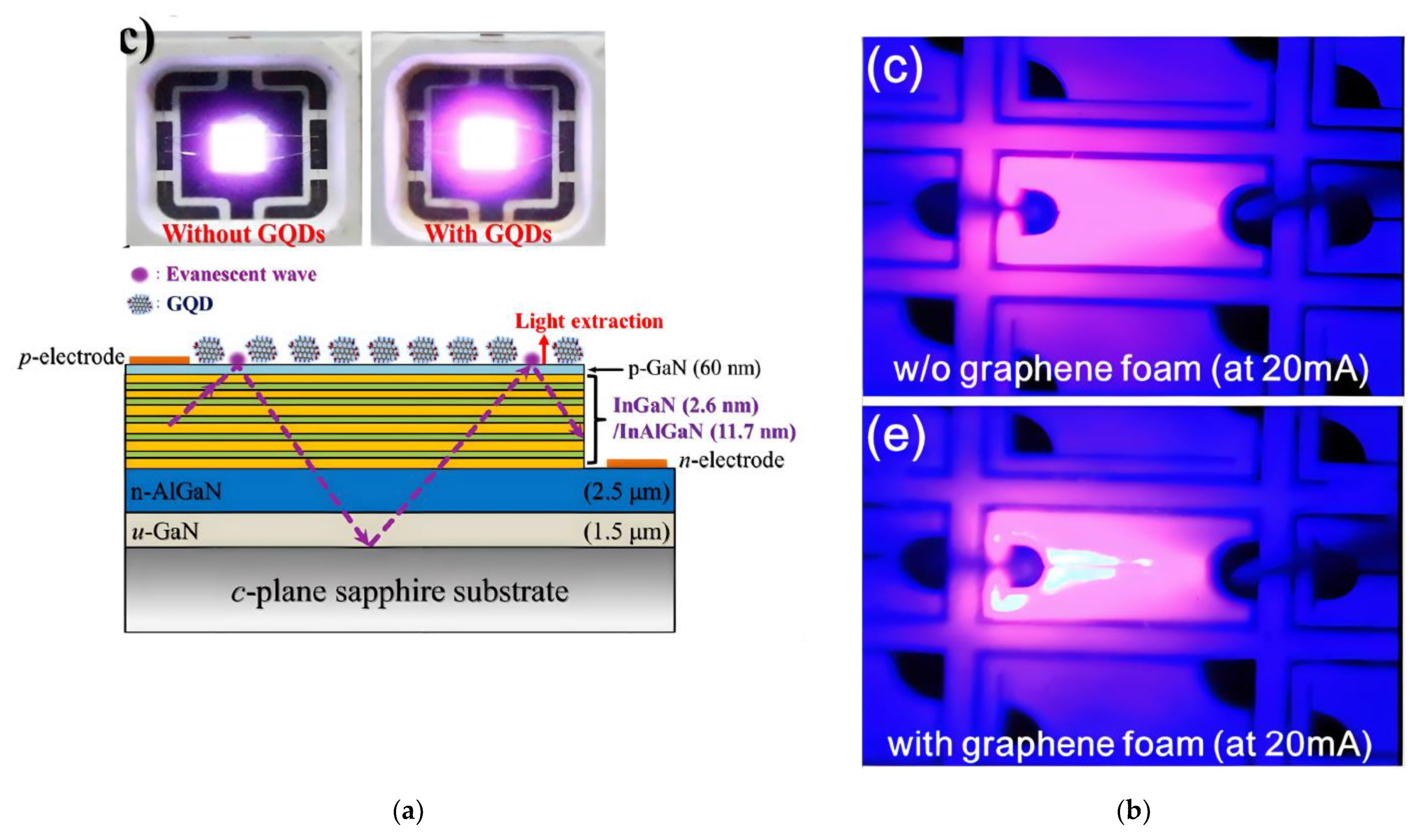
Figure 6.
Current flow through path A (solid line) and path B (dashed line) in a typical GaN-based LED.
Figure 6.
Current flow through path A (solid line) and path B (dashed line) in a typical GaN-based LED.

Figure 7.
Graphene doped with metal-chlorides integrated as TCSL into GaN-based MQW LEDs: (a) work function of doped graphene films as function of AuCl3 concentration; (b) light emission images in a typical LED device with different dopants in graphene, namely AuCl3, IrCl3 and RhCl3 compared to pristine graphene (P-G) from top to bottom, and at various current levels, namely 1 mA, 2 mA and 5 mA from left to right. (a) Reproduced with permission from [73]. Copyright 2012 IOP Publishing Ltd. (b) Reproduced with permission from [38]. Copyright 2014 The Royal Society of Chemistry.
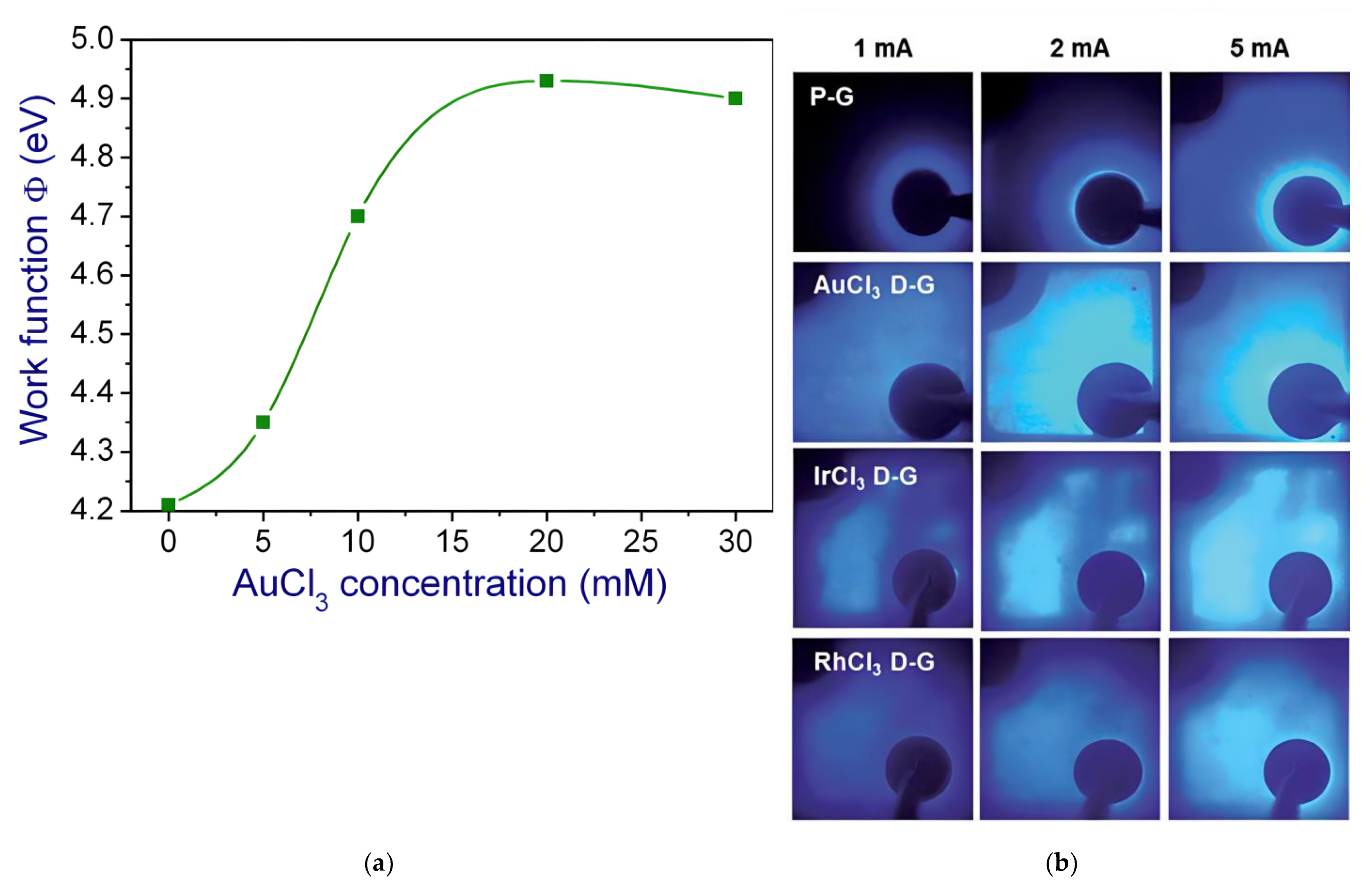
Figure 8.
Graphene doped by HNO3 acid as TCSL integrated into GaN-based LEDs: (a) I-V characteristic and (b) light emission images at an injection current of 5 mA with three different p-contacts: Cr/Au without TCSL (blue triangles and structure I), Cr/Au/graphene (green squares and structure II) and Cr/Au/doped graphene (red dots and structure III). Reproduced with permission from [98]. Copyright 2013 IOP Publishing Ltd.

Figure 9.
Graphene with NiOx interlayer as TCSL in GaN-based MQW LEDs: (a) transmission spectra of different layer combinations: NiOx (1 nm and 2 nm), NiOx/graphene, graphene, NiOx/ITO, and 280 nm ITO; (b) cross-sectional image (upper left) and EL images of LEDs with different TCSLs: NiOx (upper right), graphene (lower left), and NiOx/graphene (lower right). (a) Reproduced with permission from [35] Copyright 2012 The Royal Society of Chemistry. (b) Reproduced with permission from [15]. Copyright 2015 Elsevier Ltd.

Figure 10.
Graphene as TCSL in nanopillar MQW LEDs. (a) Scanning electron microscopy image of the nanopillars with highly homogeneous multilayer graphene; (b) light output power as a function of input current level with graphene (red circles) and graphene/Al2O3 (blue diamonds). The inset shows the respective EL spectra. (a) Reproduced with permission from [102]. Copyright 2011 The Royal Society of Chemistry. (b) Reproduced with permission from [105]. Copyright 2016 IOP Publishing Ltd.

Figure 11.
Graphene as TCSL in core-shell nanowire MQW LEDs: (a) EL (inset) and I-V characteristic (main plot) in a single nanowire LED with graphene (left) and schematic image of the nanowire structure (right); (b) SEM image of graphene transferred 3 (left) and 4 (right) times onto a large-area pyramid core-shell nanowire LED. (a) Reproduced with permission from [109]. Copyright 2014 American Chemical Society. (b) Reproduced with permission from [108]. Copyright 2013 The Japan Society of Applied Physics.


Table 1.
Usage of transferred single layer (SLG), few-layer (FLG) and multilayer (MLG) graphene TCSLs in GaN-based LEDs. Transmittance values of TCSLs are measured at (@) a certain wavelength or in a spectral range, and the electrical parameters are measured at (@) a certain input current.
Table 1.
Usage of transferred single layer (SLG), few-layer (FLG) and multilayer (MLG) graphene TCSLs in GaN-based LEDs. Transmittance values of TCSLs are measured at (@) a certain wavelength or in a spectral range, and the electrical parameters are measured at (@) a certain input current.
| TCSL | Process | T (%) | EL (nm) | Performance Comparison | |||
|---|---|---|---|---|---|---|---|
| SLG | CVD on Cu [49] | - | - | ~95 @ 460 nm | 460 | 5.87 | = 3.4V @ 20 mA: LOPSLG = 125%LOP250nm ITO |
| CVD on Cu [33] | 994–1400 | ≈10−1 | ≥95 @ 350–800 nm | 450 | >5 | LOP SLG < LOP5nmNi/5nm Au @ 0–350 mA | |
| CVD on Cu [52] | 810 | - | >90 @ 300–800 nm | 380–400 | 5.9 | = 3.92 V | |
| CVD on Cu [15] | - | 260 Ω | ~92 @ 400–700 nm | blue-purple | 6.4 | @ 20 mA: ELSLG ≈ 57%EL200 nm ITO | |
| CVD on Cu [44] | 658 | - | 97 @ 380 nm | 380 | 5.2 HD5.7 LD | @ 20 mA: ELSLG/HD ≈ 164%ELSLG/LD | |
| FLG | Scotch-tape [22] | - | - | - | 368 | 26.5 @ 1 mA | SQW vertical LEDs |
| CVD on Cu [23] | 280–850 [51,55] | - | ≥80 @ 300–800 nm | 372 | 10 @ 5 mA | SQW@ 10 V: IFLG > Iw/o FLG | |
| vertical cold wall CVD on Cu [54] 3LG | 300–350 | - | ≥81.9 @ 320–780 nm | blue | 6.76 | = 3.60 V | |
| CVD on Cu [38] 4LG | 220 | - | 87 b, 85 a @ 470 nm | - | 5.9 @ 10 mA | ICP damage | |
| CVD on CNT/Cu [56] | 1122 | - | 95 @ 400–800 nm | 452 | 6.93 | LOPFLG = 0.52 mW @ 4 mA | |
| CVD on Cu [50] | 290 | - | ~78 (ITO)~90 (2LG) @ 380 nm | 380 | 5.9 | = 4.35 V LOP2LG = 140%LOPITO @ 100 mA | |
| MLG | CVD on Ni [51] | 620 | - | 85 @ 400–800 nm | 443 | 5.6 | = 3.8 V LOPMLG = 63%LOPITO |
| CVD on Cu [59] | - | 0.220.59 1 | 96 @ 550 nm | 495 | ≥5.38 | ||
| CVD on Ni [33] | 108–80 | 0.058 | 15 @ 450 nm | 450 | 3.1 | >35LG | |
| 3D foam | CVD on 3D Cu [46] | 800 | - | 71 @ 438 nm | 438 | 4.85 @ 100 mA | @ 100 mA: EL3Dfoam = 114%ELw/o 3Dfoam LOP3Dfoam > LOPw/o 3Dfoam |
| 0D graphene quantum dots (GQD) | Pulsed laser ablation [45] | - | - | - | 387 | - | LOPGQD > LOPw/o GQD EQEGQD = 11.8% EQEw/o GQD = 6.9% @100 mA |
| Hydrothermal method [60] | - | - | - | 450 | 2.58 | LOPGQD = 125%LOPw/o GQD EQEGQD = 7.5% @15 mA |
1 RTA. a after or b before inductively coupled plasma (ICP) etching. HD heavily or LD lightly doped p-GaN layer is applied.
Table 2.
Usage of directly grown graphene (Gr) TCSLs in GaN-based LEDs.
| TCSL | Process | T (%) | EL (nm) | Performance Comparison | |||
|---|---|---|---|---|---|---|---|
| Gr | CCG @ 240 °C, MLG [63] | 2200 | - | ≥85 @ 200–800 nm | 460 | 6.4 | ~3.64 V |
| CCG @ 240 °C, MLG [50] | 2200 | - | ≥85 @ 200–700 nm | 380 | - | = 4.35 V | |
| PECVD @ 600 °C, 5–6 L [67] | 1400 | 0.15 | ≥65 @ 350–800 nm | 365 | 4.1 | LOP= 7.46 mW @ 20 mA | |
| Annealing of a-C @ 700 °C MLG [64] | 6000 | - | 84.5 @ 260 nm 91.1 @ 550 nm | blue | 10 @ 0.4 mA | W/Ni catalyst | |
| PECVD on Co @ 600 °C [65] | - | - | >65 @ 400–1000 nm | - | 5.2 | = 7.7 V | |
| PECVD ≤800 °C 1 [68] | 1020–1300 | - | >88 @ 350–750 nm | blue | 4.4 1 | = 5.1 V | |
| PECVD on Co @ 700 °C [66] | - | - | >85 @ 400–1000 nm | - | 4.7 | = 7.6 V |
1 Data are from the recent work in this group.
Table 3.
Usage of hybrid graphene TCSLs combined with various ITO configurations: nanodot (ND), thin and thick films.
Table 3.
Usage of hybrid graphene TCSLs combined with various ITO configurations: nanodot (ND), thin and thick films.
| TCSL | Process | T (%) | EL (nm) | Performance Comparison | |||
|---|---|---|---|---|---|---|---|
| Gr d/ ITO ND | CCG [63] | 2200 | - | ≥85 (Gr) >90 (ITO ND) @ 200–800 nm | 460 | 3.66 | @ ≤ 60 mA: LOPGr/ITO ND ≈ LOPITO @ > 60 mA:LOPGr/ITO ND < LOPITO |
| CCG [50] | 2200 | - | ≥85 (Gr) >90 (ITO ND) @ 200–800 nm | 380 | 4.42 | @ 100 mA: LOPGr/ITO ND = 250%LOP250 nmITO | |
| 2LG/ ITO ND | CVD on Cu [50] | 290 | - | 95 @ 400–800 nm | 380 | 4.9 | @ 100 mA: LOP2LG/ITO ND = 170%LOP250 nmITO |
| 3LG/ 7–10 nm ITO | vertical cold wall CVD on Cu [54] | 300–350 | - | ≥94.5 (7–10 nm ITO) ≥81.9 (3LG) ≥78.6 (3LG/10 nm ITO) @ 320–780 nm | blue | 3.90 | = 3.60 V |
| 3.3 nm ITO/SLG | CVD on Cu [70] | - | 10−3 (ITO/SLG/p-GaN, 1) 10−2 (ITO/p-GaN, 1) | - | 453 | 3.053.14 (ITO) | @ 20 mA: LOP3.3TO/SLG = 21.2 mW LOPITO = 19 mW EQE3.3TO/SLG = 39.1% EQEITO = 35.3% |
| 150 nm ITO/SLG | CVD on Cu [71] | 739 S 41 | 0.31 (ITO/SLG/p-GaN) 0.22 (ITO/p-GaN) | >94 S @ 300–700 nm ~94 (ITO, ITO/SLG) @ 475 nm | 475 | 3.6 3.3 (ITO) | @ 100 mA: LOP150nmITO/SLG = 145%LOP150nm ITO |
1 RTA at 500 °C in N2 for 5 min. d denotes the direct growth as distinguished from transfer. S SLG.
Table 4.
Graphene combined with various metal configurations: layer, nanoparticle (NP), nanocluster (NC), nanodot (ND), nanowire (NW), nanorod (NR). Stack sequence from left to right is from upmost to p-GaN. CNT denotes carbon nanotube.
Table 4.
Graphene combined with various metal configurations: layer, nanoparticle (NP), nanocluster (NC), nanodot (ND), nanowire (NW), nanorod (NR). Stack sequence from left to right is from upmost to p-GaN. CNT denotes carbon nanotube.
| Hybrid with | Process | T (%) | EL (nm) | Performance Comparison | |||
|---|---|---|---|---|---|---|---|
| layer | CVD on Ni [31,73] MLG/2 nm Au | 1150 | 1.3(MLG/p-GaN) 0.24 (MLG/Au/ p-GaN) | averaged 72 (MLG) @ 350–800 nm | 455 | 4.63 4.26 1 | = 6.59 V |
| PECVD on Cu [57] SLG/Ni|Au (1 nm|1 nm) | - | ≥ 90 S @ 200–800 nm | blue | 3.03 (Gr/Ni|Au) | @ 20 mA: = 3.01 V LOPGr/Ni|Au = 9.36 mW LOPITO = 10.15 mW | ||
| CVD on Cu [76] 2LG/Ni|Au (1 nm|1 nm) | 760 S 380 (2LG) | - | - | - | 3.4 (2LG/Ni|Au) | = 3.6 V | |
| CVD on Cu [34] SLG/Au/Ni (1 nm/1 nm) | 100–200 | 5.5(SLG/p-GaN) 1 0.6 (SLG/Au/Ni/ p-GaN) 1 | ≥95 S ≥78 (SLG/Au/Ni) @ 350–800 nm | 446 | 3 (Gr/Au/Ni) | @ 3 V: ELSLG/Au/Ni = 500% ELSLG or bare | |
| CVD on Cu or Ni [74] SLG/2 nm Ni SLG/2 nm Au | - | 0.88(SLG/p-GaN)1 0.196 (SLG/Au/ p-GaN)1 | ≥85 (Ni) ≥80 (Au) ≥97.5 S @ 400–800 nm | blue | 4.5 S | - | |
| CVD on Cu [32] 3 nm Ni/Gr | 1250 (Gr) 690 (Ni/Gr) 1 | - | > 90 (Gr) @ 300–700 nm 75 (Ni/Gr) 86 (ITO) @ 460 nm | 460 | 6.2 (Gr) 4.8 (3Ni/Gr) | = 3.5 V @ 20 nmA: EL3Ni/Gr ≈ ELGr < ELITO | |
| CVD on Cu [32] 3 nm Ni/Gr | 1250 (Gr) 690 (Ni/Gr) 1 | - | 74 (Ni/Gr) 70 (150 nm ITO) @ 380 nm | 380 | 13.2 (Gr) 7.1 (3Ni/Gr) | = 5 V @ 5 mA: ELNi/Gr = 83% ELITO | |
| CVD on Cu [12] SLG/2 nm Au | 500 S 200(SLG/Au) | 0.08 (SLG/Au/ p-GaN) | 92.8 S 78 (SLG/Au) @ 373 nm | 373 | 7.2 S 4.25(SLG/Au) | =3.94 @ 20 mA: ELSLG/Au< ELITO | |
| CVD on Cu [75] AZO/2 nm Ni/SLG | 70 (AZO) | RC(AZO/Ni/p-GaN) | 65 (AZO/2Ni/SLG) 66 (AZO/2Ni) @ 386 nm | 386 | AZO/Ni: 4.6 S 5.8 (w/o Gr) | = 4.85 eV = 4.48 eV @50 mA: ELAZO/Ni/SLG = 195% ELAZO/Ni | |
| NP, NC, ND | CVD on Ni [24] Ag NP/MLG | - | - | 89 (MLG) 82(MLG/Ag * NP) @ 460 nm | 460 | 4.5 (MLG) 3.4 (MLG/ Ag * NP) | @ 100 mA: LOPAg NP/MLG = 270%LOPMLG |
| CVD on Cu [12] SLG/Au NC | 500 S 150(SLG/Au) | 0.018 (SLG/Au/ p-GaN) | 92.8 S 82.7 (SLG/Au) @ 373 nm | 373 | 7.2 S 4.02 (SLG/Au NC) | = 3.94 @ 20 mA: ELSLG/Au = 110% ELITO | |
| NP, NC, ND | CVD on Cu [52] SLG/Ag NC | 810 S 280 (SLG/Ag) | - | >95 S @ 300–800 nm 84 (SLG/Ag) @ 380 nm | 380–400 | 5.9 S 4.06 (SLG/Ag) | = 3.92 V @ 20 mA: ELGr/Ag ≈ ELITO |
| CVD on Cu [72] MLG/Ag NDs | 551 (MLG) | 0.25 (TCSL/p-GaN)2Ag 10−5 (TCSL/p-GaN)4Ag | 82.5 (MLG/ND)2Ag 69.5 (MLG/ND)4Ag @ 365 nm | 365 | 7.4 (MLG/ND)2Ag 5.9 (MLG/ND)4Ag | =4.2 V @ 20mA: LOPMLG/2Ag = 131%LOPMLG/4Ag | |
| NW, NR | CVD on Cu [77] ZnO NW/SLG | 100–200 | 5 ZnO/SLG/p-GaN | 97 S 90 (ZnO NW/SLG) @ 450–800 nm | 446 | 2.7(ZnO/SLG) 2.9 (ZnO) @ 7.5 mA | @ 2.8 V: LOPZnO/SLG = 166%LOPSLG-LED |
| CVD on Cu [78] 2–3LG/Ag NW | 1350 (FLG) 367 (FLG/Ag NW) | 1.06 Ωcm (FLG/p-GaN) 0.105 Ωcm (FLG/Ag/p-GaN) | 96.2 (Ag NW) 92.8 (FLG/Ag NW) @ 550 nm | blue | 11.8 (FLG) 6.6 (FLG/Ag) | @ 20 mA: LOP2–3LG/Ag = 295% LOP2–3LG | |
| CVD on Cu [79] SLG/Ag NW | 500 S 50 (Ag NW) 30 (SLG/Ag) | - | 93 S 90.2 (Ag NW) 86.3 (SLG/Ag NW) @ 375 nm | 375–378 | 10.9 S 6.7 (Ag NW) 4.48 (SLG/Ag) | @ 20 mA: ELSLG/Ag NW = 589% ELSLG | |
| CVD on CNT/Cu [56] 3LG-CNT | 1122 (3LG) 533 (3LG-CNT) | - | 95 (3LG) 88 (3LG-CNT) @ 400–800 nm | 452 | 6.12 (3LG-CNT) 6.93 (3LG) | @ 4 mA LOP3LG = 0.52 mW LOP3LG-CNT = 1.3 mW |
1 RTA. S SLG. * Patterned micro-circle. 4Ag or 2Ag denotes ND formed by a 2 nm or 4 nm thin Ag film.
Table 5.
Usage of p-type doped graphene (p-Gr) as TCSL in GaN-based LEDs. The doping concentration is given in mM.
Table 5.
Usage of p-type doped graphene (p-Gr) as TCSL in GaN-based LEDs. The doping concentration is given in mM.
| TCSL | Process | T (%) | EL (nm) | Performance Comparison | |||
|---|---|---|---|---|---|---|---|
| SLG/ Ga:ZnO (GZO) | CVD [97] AuCl3 doping | 170 (20–30 mM) | - | ≥ 80 (2.5–30 mM) @ 425 nm | 425 | - | @ 10 mA: ELp-SLG/GZO ≥ 220%ELGZO |
| BLG | CVD on Cu [94] AuCl3 doping | - | 0.24 (p-BLG/p-GaN) 1.3(BLG/p-GaN) | 92 (BLG) 88.5(10 mM) @ 380 nm | 380 | 3.98 (10 mM) 5.85 (BLG) | = 3.92 V @ 100 mA: ELp-BLG = 120%EL200 nm ITO = 4.90 eV = 4.51 eV |
| FLG | CVD on Cu [93] 3LGA uCl3 doping | 466.1 (3LG) 175.5 (5 mM 1) 158.5 (10 mM 1) 112.4 (20 mM 1) | - | 87.9 (3LG) 86.4–85.1–82.9 (5–10–20 mM) @ 363 nm | 363 | @ 6.5 V ≈ 0.65 mA ≈ 1.5–3 mA | ELp-3LG ≥ EL3LG |
| CVD on Cu [38] 4LG AuCl3 doping | 780 S 220 (4LG) 105–140 (20 mM) | - | 96 S,b 87 (4LG) b 83–84 (20 mM) b @ 470 nm | - | - | = 4.9–5.1 eV = 4.2 eV | |
| MLG | CVD on Ni [36] 9LG AuCl3 doping | 1000 (9LG) 203 (5 mM) 103 (20 mM) | - | 89 (9LG) 85 (5 mM) 78 (20 mM) @ 400 nm | 400 | 4.73 (9LG) 3.94 (5 mM) 3.86 (20 mM) @ 0.4 mA | @ 0.5 mA: ELp-9LG = 193.8%EL9LG = 4.77–5.12 eV = 4.42 eV |
| CVD on Ni [31,73] >12LGA uCl3 doping | 1150 (MLG) 476 (20 mM) | 1.3 (MLG/ p-GaN) 0.4 (doped MLG/p-GaN 0.24(MLG/Au/p-GaN) | 72 A (MLG) ~67.5 (20 mM) @ VIS | blue | 6.59 (MLG) 5.55 (p-MLG) 4.63(MLG/Au) 4.26(MLG/Au 1) 3.96 (p-MLG/Au 1) | = 4 V = 5.1 eV = 4.21–4.24 eV = 4.93 eV | |
| CVD on Ni [98] ≈10LG HNO3 doping | - | - | - | ~3.9 (w/o TCSL) ~5 (10LG) ~4.25 (p-10LG) | = 4.21 eV = 4.93 eV LOPw/o Gr = 8.67 mW LOP10LG = 12.34 mW LOPp-10LG = 17.83 mW @ 80 mA |
1 RTA. A Averaged value. b before ICP. S SLG. w/o TCSL denotes without TCSL.
Table 6.
Usage of graphene combined with NiOx as TCSL in GaN-based LEDs.
| TCSL | Process | T (%) | EL (nm) | Performance Comparison | |||
|---|---|---|---|---|---|---|---|
| SLG/ NiOx | CVD on Cu [15] NiOx: 3 nm Ni RTA in air | - | 260 Ω (SLG/p-GaN) 2000 Ω (NiOx/p-GaN) 75 Ω (SLG/NiOx/p-GaN) | >91 S >89 (NiOx) >81(SLG/NiOx) @ 400–700 nm | blue | 6.4 (SLG) 4.5 (SLG/NiOx) 3.9 (ITO) | = 5.5–5.9 eV @ 20 mA: ELSLG/NiOx = 85% EL200nm ITO = 150% ELSLG |
| CVD on Cu or Ni [74] 2 nm NiOx: Ni RTA in O2 ambient | - | 10−1 (Gr/p-GaN, 1) | ≥97.5 S ≥95.5(SLG/NiOx) ≥90.5 (SLG/NiOx,1) @ 400–800 nm | blue | 4.5 (Gr) 3.16 (Gr/NiOx) 3.6 (NiOx) | ≈ 5.53 e V@ 20 mA: LOP Gr/NiOx1 ≈ 70%LOPGr | |
| FLG/ NiOx | CVD on Cu [35] 2–3L G1–2 nm NiOx: Ni RTA in air | >10 kΩ (1–2 nm NiOx) ~1.2 kΩ (FLG, FLG/1 nm NiOx, FLG/2 nm NiOx) | 10−4 (Gr/NiOx/p-GaN) 10−2–10−1 (Gr/p-GaN)10−3 (ITO/(NiOx)/p-GaN) | 90–83 (1–2 nm NiOx) >95 (FLG) >85(FLG/1NiOx) >78(FLG/2NiOx) @ 350–800 nm | blue | 6.15 (FLG) 3.65 (FLG/NiOx) 3.2 (ITO) | @ 20 mA: LOP280 nm ITO ≥ LOPFLG/NiOx = 157%LOPFLG |
| CVD [100] 3LG NiOx: 2 nm Ni RTA, N2:O2 = 4:1 | - | 10−4 (Gr/NiOx/p-GaN, 1 550 °C) | >95 (FLG/NiOx) @ 400–800 nm FLG/NiOx,1: 93.6 (350 °C) 88.6 (450 °C) 87 (550 °C) @ 450 nm | 450 | 5.4 (FLG) FLG/NiOx,1: 4.4 (350 °C) 3.9 (450 °C) 3.5 (550 °C) | = 4.56 eV = 4.98 eV = 4.67 eV @ 100 mA: LOPFLG/NiOx,350 °C > LOPNi/Au > LOPFLG/NiOx, 550 °C | |
| FLG- CNT/ NiOx | CVD on CNT/Cu [56] 3LG2 nm NiOx | 1122 (3LG) 1110(3LG/CNT) * 533 (3LG-CNT) ** | - | 95 (3LG) 95 (2NiOx) 88 (3LG/CNT) ** @ 400–800 nm | 452 | 6.93 (3LG) 6.12 (3LG-CNT) 5.12 (3LG-CNT/NiOx) | ≈ 5.1 eV @ 4 mA: LOP3LG = 0.52 mW LOP3LG-CNT = 1.30 mW LOP3LG-CNT/NiOx = 2.08 mW |
| MLG/ NiOx | CVD on Ni [33] >35LG 2 nm NiOx | 994–1400 S 108–80 (MLG) 1338 (MLG2) 37 (Ni) ≈300 (3LG) | 10−4 (Ni/Au/p-GaN) 10−2 (MLG/p-GaN) 10−1 (MLG 2/p-GaN) 10−2 (MLG/ NiOx/p-GaN) ≤10−1 (SLG/p-GaN) | ≥97.5 S ≥98 (2NiOx) 89 (3LG) 87 (3LG/NiOx) 71 (Ni/Au) 15 (MLG) @ 450 nm | 450 | ≈3.1 (MLG/NiOx) 3.2 (3LG/NiOx) ≈3.1 (MLG)2.9 (Ni/Au) >5 (SLG) 3.37–3.47( SLG/NiOx) | @ 100 mA: LOP3LG/NiOx > LOPNi/Au > LOPSLG > LOPMLG/NiOx |
1 RTA after graphene transfer. 2 O2 plasma thinned MLG. * Stacked layers. ** Composed layers. S SLG.
Table 7.
Usage of graphene as TCSL used in advanced GaN-based LEDs.
| Device | Process | T (%) | EL (nm) | Performance Comparison | |||
|---|---|---|---|---|---|---|---|
| 1D nano-pillar | CVD on Cu MLG, RTA1 [102] | 550 S 215 (MLG) | - | 96 S 87 (MLG)@ 450 nm | 451 | 4.6 | mechanically robust no EL shift |
| nanorod (NR) | CVD on Cu MLG transfer before (I) and after (II) ICP, RTA1 in N2, 200 °C, 15 min [103] | - | - | - | 456 | 11.5 (w/o Gr) 8.9 (I) 7.0 (II) | @ 20 mA: ELII = 155.3%ELI |
| Rapid CVD on Cu FLG [101] | 3000 S 1000 (3LG)[54] 300 (3LG) on ND | 0.8–1.8 (Au/Ti/3LG/p-GaN) | 81.9 (3LG) @ 320 nm [54] | blue | 5.2 (ND) 6.7 (flat mesa) | WPE3LG-ND = 5.2% > WPENi/Au-ND @ 20 mA: LOP3LG-ND = 132%LOP3LG-flat mesa | |
| CVD on Cu MLG [105] | - | - | - | 405 | 5.5 (KOH and KOH/ALD) @ 1 mA | PLKOH+ALD = 130%PLKOH = 180%PLas etched ELKOH+ALD = 130%ELKOH | |
| Air hole photonic crystal (PC) | CVD 2LG [104] | ~600 S ~300 (2LG) on planar SiO2 107 (2LG) on PC | - | nearly 95 (2LG) 85 (Ni/Au/2LG) @ 460 nm | - | planar LEDs: 3.3 (w. 2LG) 4.3 (w/o Gr) PC LEDs: 3.4 (w. 2LG) 4 S 4.9 (w/o Gr) | @ 20 mA: LOP2LG PC = 6.2 mW LOP2LG,planar =4.5 mW LOP PC = 3.8 mW |
| Core-shell | CVD on Cu MLG RTA1 [108] | - | - | ≥9 5@ 425–800 nm | 478 | 8.8 | Current spreading improved |
| CVD on Cu SLG [109] | - | - | - | 494 2 415 3 | 4 (turn-on) | EL appears at 6 V, 0.16 µA |
1 RTA after graphene transfer. 2 Low current injection. 3 High current injection. S SLG.
Publisher’s Note: MDPI stays neutral with regard to jurisdictional claims in published maps and institutional affiliations. |
© 2022 by the authors. Licensee MDPI, Basel, Switzerland. This article is an open access article distributed under the terms and conditions of the Creative Commons Attribution (CC BY) license (https://creativecommons.org/licenses/by/4.0/).
Share and Cite
MDPI and ACS Style
Zhang, H.; Mischke, J.; Mertin, W.; Bacher, G. Graphene as a Transparent Conductive Electrode in GaN-Based LEDs. Materials 2022, 15, 2203. https://doi.org/10.3390/ma15062203
AMA Style
Zhang H, Mischke J, Mertin W, Bacher G. Graphene as a Transparent Conductive Electrode in GaN-Based LEDs. Materials. 2022; 15(6):2203. https://doi.org/10.3390/ma15062203
Chicago/Turabian StyleZhang, Hehe, Jan Mischke, Wolfgang Mertin, and Gerd Bacher. 2022. "Graphene as a Transparent Conductive Electrode in GaN-Based LEDs" Materials 15, no. 6: 2203. https://doi.org/10.3390/ma15062203
Note that from the first issue of 2016, this journal uses article numbers instead of page numbers. See further details here.