
Impact of the RF Power on the Copper Nitride Films Deposited in a Pure Nitrogen Environment for Applications as Eco-Friendly Solar Absorber
 , and
, and
Abstract
:1. Introduction
2. Materials and Methods
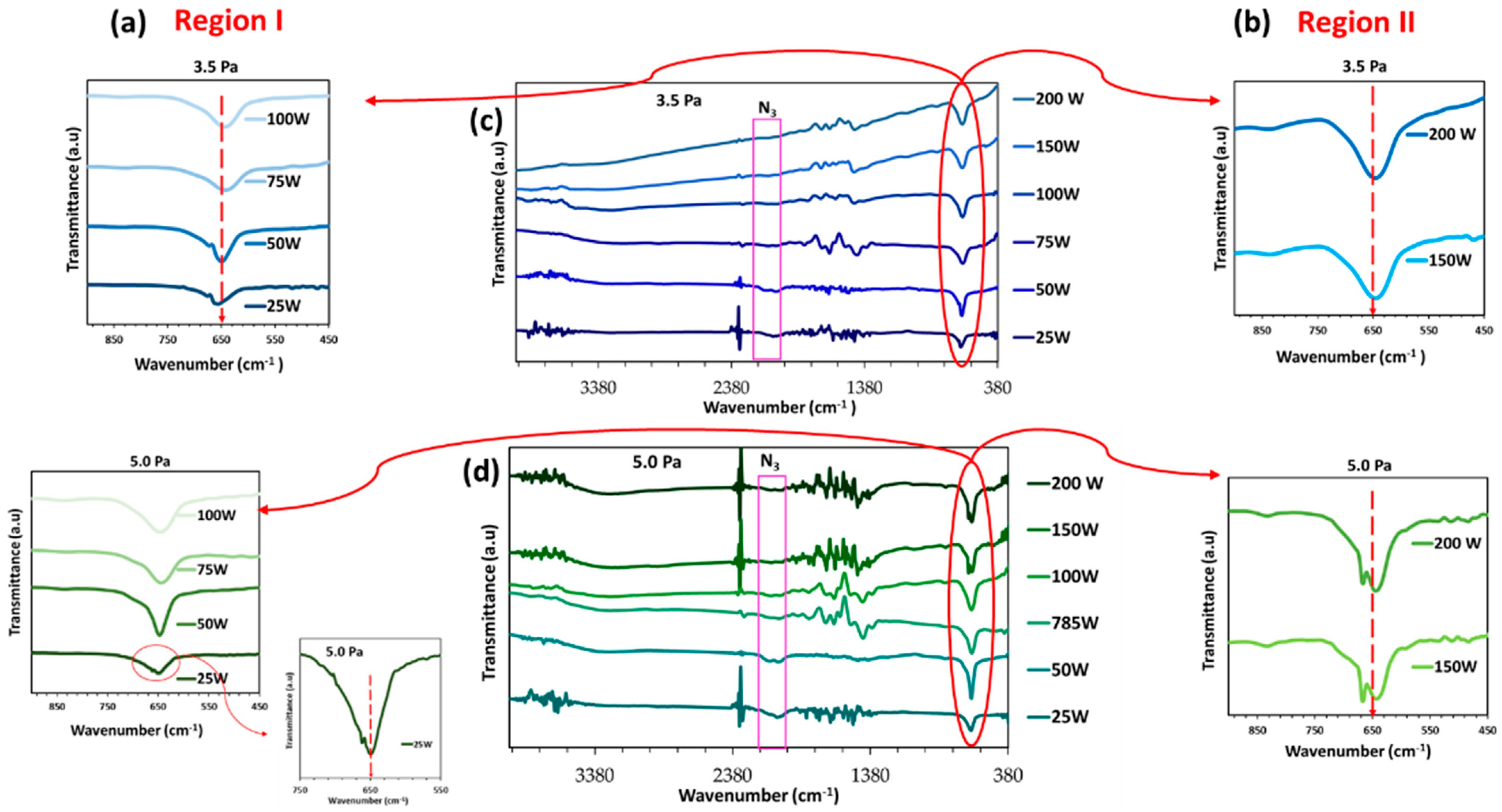
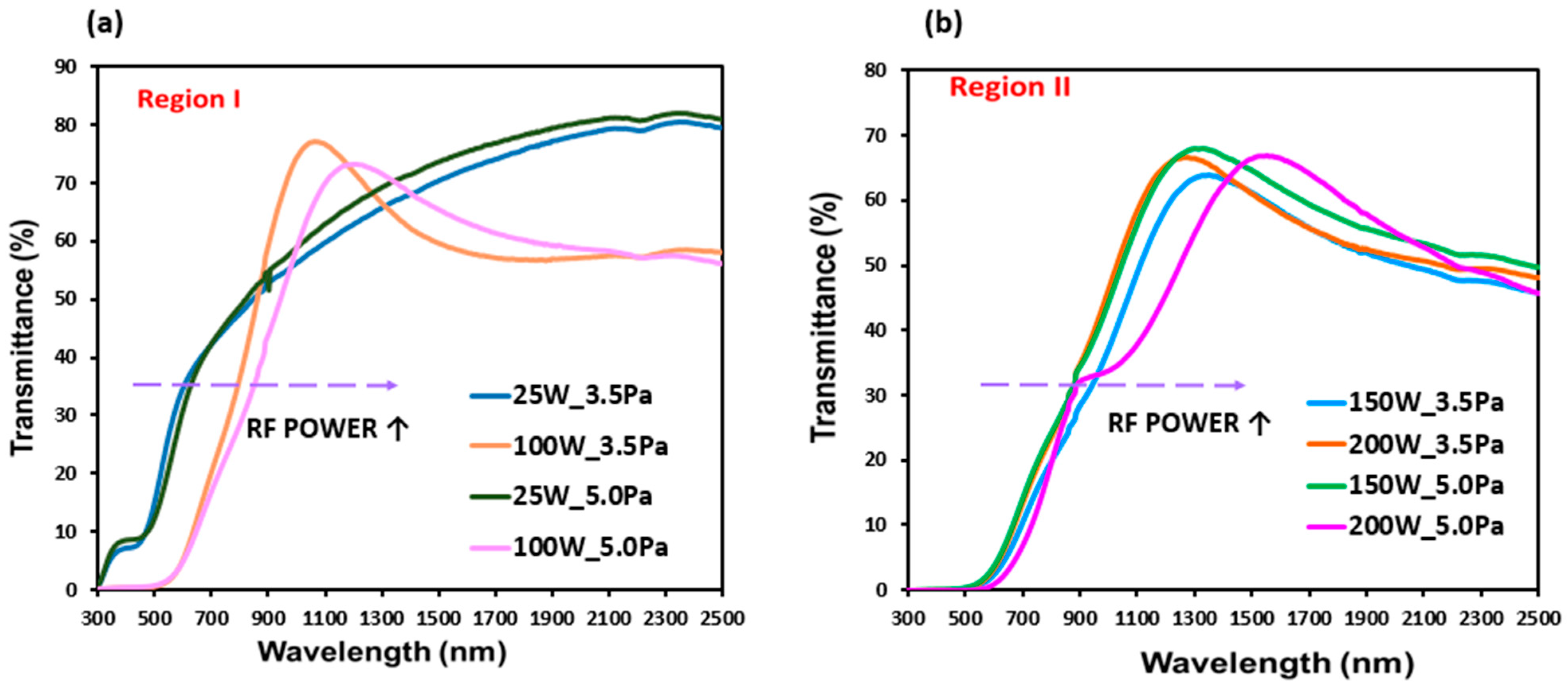
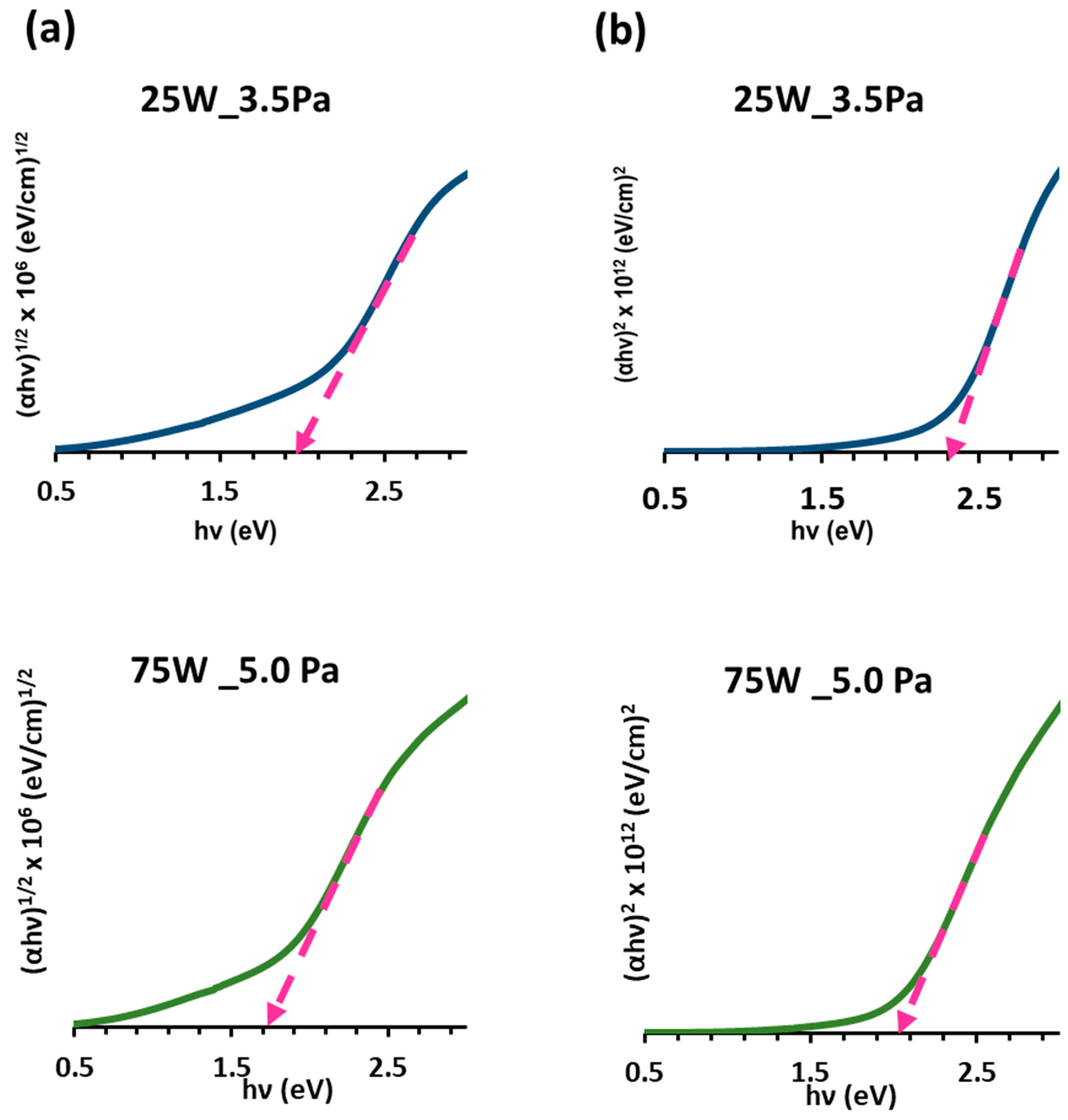
3. Results and Discussion
4. Conclusions
Author Contributions
Funding
Informed Consent Statement
Data Availability Statement
Acknowledgments
Conflicts of Interest
References
- Zakutayev, A. Design of nitride semiconductors for solar energy conversion. J. Mater. Chem. A 2016, 4, 6742–6754. [Google Scholar] [CrossRef]
- Borsa, D.M.; Boerma, D.O. Growth, structural and optical properties of Cu3N films. Surf. Sci. 2004, 548, 95–105. [Google Scholar] [CrossRef]
- Jiang, A.; Qi, M.; Xiao, J. Preparation, structure, properties, and application of copper nitride (Cu3N) thin films: A review. J. Mater. Sci. Technol. 2018, 34, 1467–1473. [Google Scholar] [CrossRef]
- BOUAZZA, A. Deposition of Thin Films Materials used in Modern Photovoltaic Cells. Int. J. Thin Film Sci. Technol. 2022, 11, 313–320. [Google Scholar] [CrossRef]
- Paredes, P.; Rauwel, E.; Rauwel, P. Surveying the Synthesis, Optical Properties and Photocatalytic Activity of Cu3N Nanomaterials. Nanomaterials 2022, 12, 2218. [Google Scholar] [CrossRef]
- Tilemachou, A.; Zervos, M.; Othonos, A.; Pavloudis, T.; Kioseoglou, J. p-Type Iodine-Doping of Cu3N and Its Conversion to γ-CuI for the Fabrication of γ-CuI/Cu3N pn Heterojunctions. Electron. Mater. 2022, 3, 15–26. [Google Scholar] [CrossRef]
- Hahn, U.; Weber, W. Electronic structure and chemical-bonding mechanism of Cu3N, Cui3NPd, and related Cu (I) compounds. Phys. Rev. B 1996, 53, 12684. [Google Scholar] [CrossRef]
- Ghoohestani, M.; Karimipour, M.; Javdani, Z. The effect of pressure on the physical properties of Cu3N. Phys. Scr. 2014, 89, 035801. [Google Scholar] [CrossRef]
- Sahoo, G.; Meher, S.; Jain, M.K. Room temperature growth of high crystalline quality Cu3N thin films by modified activated reactive evaporation. Mater. Sci. Eng. B 2015, 191, 7–14. [Google Scholar] [CrossRef]
- Matsuzaki, K.; Okazaki, T.; Lee, Y.-S.; Hosono, H.; Susaki, T. Controlled bipolar doping in Cu3N (100) thin films. Appl. Phys. Lett. 2014, 105, 222102. [Google Scholar] [CrossRef]
- Caskey, C.M.; Richards, R.M.; Ginley, D.S.; Zakutayev, A. Thin film synthesis and properties of copper nitride, a metastable semiconductor. Mater. Horiz. 2014, 1, 424–430. [Google Scholar] [CrossRef]
- Li, S.; Hao, J.; Yu, S. Mechanical properties of cubic Cu3N and Cu4N: A theoretical investigation. Vacuum 2021, 191, 110366. [Google Scholar] [CrossRef]
- Yamada, N.; Maruya, K.; Yamaguchi, Y.; Cao, X.; Ninomiya, Y. P-to n-type conversion and nonmetal–metal transition of lithium-inserted Cu3N Films. Chem. Mater. 2015, 27, 8076–8083. [Google Scholar] [CrossRef]
- Jiang, A.; Xiao, J.; Gong, C.; Wang, Z.; Ma, S. Structure and electrical transport properties of Pb-doped copper nitride (Cu3N: Pb) films. Vacuum 2019, 164, 53–57. [Google Scholar] [CrossRef]
- Gao, L.; Ji, A.; Zhang, W.; Cao, Z. Insertion of Zn atoms into Cu3N lattice: Structural distortion and modification of electronic properties. J. Cryst. Growth 2011, 321, 157–161. [Google Scholar] [CrossRef]
- Borsa, D.; Grachev, S.; Presura, C.; Boerma, D. Growth and properties of Cu 3 N films and Cu 3 N/γ′-Fe 4 N bilayers. Appl. Phys. Lett. 2002, 80, 1823–1825. [Google Scholar] [CrossRef]
- Miura, A.; Takei, T.; Kumada, N. Synthesis of Cu3N from CuO and NaNH2. J. Asian Ceram. Soc. 2014, 2, 326–328. [Google Scholar] [CrossRef]
- Zervos, M.; Othonos, A.; Pavloudis, T.; Giaremis, S.; Kioseoglou, J.; Mavridou, K.; Katsikini, M.; Pinakidou, F.; Paloura, E.C. Impact of Oxygen on the Properties of Cu3N and Cu3–x N1–x O x. J. Phys. Chem. C 2021, 125, 3680–3688. [Google Scholar] [CrossRef]
- Hou, Z. Effects of Cu, N, and Li intercalation on the structural stability and electronic structure of cubic Cu3N. Solid State Sci. 2008, 10, 1651–1657. [Google Scholar] [CrossRef]
- Sakalley, S.; Saravanan, A.; Cheng, W.-C.; Chen, S.-C.; Sun, H.; Hsu, C.-L.; Huang, B.-R. High power impulse magnetron sputtering growth processes for copper nitride thin film and its highly enhanced UV—Visible photodetection properties. J. Alloys Compd. 2022, 896, 162924. [Google Scholar] [CrossRef]
- Zhu, L.; Gong, C.; Xiao, J.; Wang, Z. Photocatalytic properties of copper nitride/molybdenum disulfide composite films prepared by magnetron sputtering. Coatings 2020, 10, 79. [Google Scholar] [CrossRef]
- Ali, H.T.; Tanveer, Z.; Javed, M.R.; Mahmood, K.; Amin, N.; Ikram, S.; Ali, A.; Gilani, M.R.H.S.; Sajjad, M.A.; Yusuf, M. A new approach for the growth of copper nitrides thin films by thermal evaporation using nitrogen as source gas. Optik 2021, 245, 167666. [Google Scholar] [CrossRef]
- Gonzalez-Arrabal, R.; Gordillo, N.; Martin-Gonzalez, M.; Ruiz-Bustos, R.; Agulló-López, F. Thermal stability of copper nitride thin films: The role of nitrogen migration. J. Appl. Phys. 2010, 107, 103513. [Google Scholar] [CrossRef]
- Rahmati, A.; Ghoohestani, M.; Badehian, H.; Baizaee, M. Ab. initio study of the structural, elastic, electronic and optical properties of Cu3N. Mater. Res. 2014, 17, 303–310. [Google Scholar] [CrossRef]
- Gallardo-Vega, C.; De la Cruz, W. Study of the structure and electrical properties of the copper nitride thin films deposited by pulsed laser deposition. Appl. Surf. Sci. 2006, 252, 8001–8004. [Google Scholar] [CrossRef]
- Asano, M.; Umeda, K.; Tasaki, A. Cu3N thin film for a new light recording media. Jpn. J. Appl. Phys. 1990, 29, 1985. [Google Scholar] [CrossRef]
- Li, Z.; Gordon, R.G. Thin, continuous, and conformal copper films by reduction of atomic layer deposited copper nitride. Chem. Vap. Depos. 2006, 12, 435–441. [Google Scholar] [CrossRef]
- Gordillo, N.; Gonzalez-Arrabal, R.; Martin-Gonzalez, M.S.; Olivares, J.; Rivera, A.; Briones, F.; Agulló-López, F.; Boerma, D.O. DC triode sputtering deposition and characterization of N-rich copper nitride thin films: Role of chemical composition. J. Cryst. Growth 2008, 310, 4362–4367. [Google Scholar] [CrossRef]
- Chen, S.-C.; Huang, S.-Y.; Sakalley, S.; Paliwal, A.; Chen, Y.-H.; Liao, M.-H.; Sun, H.; Biring, S. Optoelectronic properties of Cu3N thin films deposited by reactive magnetron sputtering and its diode rectification characteristics. J. Alloys Compd. 2019, 789, 428–434. [Google Scholar] [CrossRef]
- Pierson, J. Structure and properties of copper nitride films formed by reactive magnetron sputtering. Vacuum 2002, 66, 59–64. [Google Scholar] [CrossRef]
- Wilczopolska, M.; Nowakowska-Langier, K.; Okrasa, S.; Skowronski, L.; Minikayev, R.; Strzelecki, G.W.; Chodun, R.; Zdunek, K. Synthesis of copper nitride layers by the pulsed magnetron sputtering method carried out under various operating conditions. Materials 2021, 14, 2694. [Google Scholar] [CrossRef]
- Okrasa, S.; Wilczopolska, M.; Strzelecki, G.; Nowakowska-Langier, K.; Chodun, R.; Minikayev, R.; Król, K.; Skowronski, L.; Namyślak, K.; Wicher, B. The influence of thermal stability on the properties of Cu3N layers synthesized by pulsed magnetron sputtering method. Thin Solid Film. 2021, 735, 138889. [Google Scholar] [CrossRef]
- Figueira, C.; Rosario, G.D.; Pugliese, D.; Rodríguez-Tapiador, M.; Fernández, S. Effect of Argon on the Properties of Copper Nitride Fabricated by Magnetron Sputtering for the Next Generation of Solar Absorbers. Materials 2022, 15, 8973. [Google Scholar] [CrossRef]
- Wang, J.; Chen, J.; Yuan, X.; Wu, Z.; Miao, B.; Yan, P. Copper nitride (Cu3N) thin films deposited by RF magnetron sputtering. J. Cryst. Growth 2006, 286, 407–412. [Google Scholar] [CrossRef]
- Nowakowska-Langier, K.; Chodun, R.; Minikayev, R.; Okrasa, S.; Strzelecki, G.W.; Wicher, B.; Zdunek, K. Phase composition of copper nitride coatings examined by the use of X-ray diffraction and Raman spectroscopy. J. Mol. Struct. 2018, 1165, 79–83. [Google Scholar] [CrossRef]
- Yuan, X.; Yan, P.; Liu, J. Preparation and characterization of copper nitride films at various nitrogen contents by reactive radio-frequency magnetron sputtering. Mater. Lett. 2006, 60, 1809–1812. [Google Scholar] [CrossRef]
- Meymian, M.R.Z.; Heravi, A.D.; Mehr, A.K. Influence of bias voltage on optical and structural characteristics of Cu3N films deposited by reactive RF magnetron sputtering in a pure nitrogen atmosphere. Mater. Sci. Semicond. Process. 2020, 112, 104995. [Google Scholar] [CrossRef]
- Pierson, J. Influence of bias voltage on copper nitride films deposited by reactive sputtering. Surf. Eng. 2003, 19, 67–69. [Google Scholar] [CrossRef]
- Cao, Z. Thin Film Growth for Thermally Unstable Noble-Metal Nitrides by Reactive Magnetron Sputtering. In Thin Film Growth; Elsevier: Amsterdam, The Netherlands, 2011; pp. 185–210. [Google Scholar] [CrossRef]
- Du, Y.; Ji, A.; Ma, L.; Wang, Y.; Cao, Z. Electrical conductivity and photoreflectance of nanocrystalline copper nitride thin films deposited at low temperature. J. Cryst. Growth 2005, 280, 490–494. [Google Scholar] [CrossRef]
- Hadian, F.; Rahmati, A.; Movla, H.; Khaksar, M. Reactive DC magnetron sputter deposited copper nitride nano-crystalline thin films: Growth and characterization. Vacuum 2012, 86, 1067–1072. [Google Scholar] [CrossRef]
- Xiao, J.; Li, Y.; Jiang, A. Structure, optical property and thermal stability of copper nitride films prepared by reactive radio frequency magnetron sputtering. J. Mater. Sci. Technol. 2011, 27, 403–407. [Google Scholar] [CrossRef]
- Gordillo, N.; Gonzalez-Arrabal, R.; Alvarez-Herrero, A.; Agullo-Lopez, F. Free-carrier contribution to the optical response of N-rich Cu3N thin films. J. Phys. D: Appl. Phys. 2009, 42, 165101. [Google Scholar] [CrossRef]
- Park, H.; Seo, H.; Kim, S.E. Anti-oxidant copper layer by remote mode N2 plasma for low temperature copper–copper bonding. Sci. Rep. 2020, 10, 21720. [Google Scholar] [CrossRef] [PubMed]
- Ścigała, A.; Szłyk, E.; Dobrzańska, L.; Gregory, D.H.; Szczęsny, R. From binary to multinary copper based nitrides–Unlocking the potential of new applications. Coord. Chem. Rev. 2021, 436, 213791. [Google Scholar] [CrossRef]
- Dorranian, D.; Dejam, L.; Sari, A.H.; Hojabri, A. Structural and optical properties of copper nitride thin films in a reactive Ar/N2 magnetron sputtering system. Eur. Phys. J. Appl. Phys. 2010, 50, 20503. [Google Scholar] [CrossRef]
- Kong, Q.; Ji, L.; Li, H.; Liu, X.; Wang, Y.; Chen, J.; Zhou, H. Influence of substrate bias voltage on the microstructure and residual stress of CrN films deposited by medium frequency magnetron sputtering. Mater. Sci. Eng. B 2011, 176, 850–854. [Google Scholar] [CrossRef]
- Xiao, J.; Qi, M.; Cheng, Y.; Jiang, A.; Zeng, Y.; Ma, J. Influences of nitrogen partial pressure on the optical properties of copper nitride films. RSC Adv. 2016, 6, 40895–40899. [Google Scholar] [CrossRef]
- Islam, M.M.; Georgiev, D.G. Stable stoichiometric copper nitride thin films via reactive sputtering. Appl. Phys. A 2022, 128, 579. [Google Scholar] [CrossRef]
- Fallberg, A.; Ottosson, M.; Carlsson, J.-O. Phase stability and oxygen doping in the Cu–N–O system. J. Cryst. Growth 2010, 312, 1779–1784. [Google Scholar] [CrossRef]
- Yu, W.; Zhao, J.; Jin, C. Simultaneous softening of Cu 3 N phonon modes along the T 2 line under pressure: A first-principles calculation. Phys. Rev. B 2005, 72, 214116. [Google Scholar] [CrossRef]
- Singh, K. Magnetic and spectroscopic studies on cupric azide. Trans. Faraday Soc. 1971, 67, 2436–2444. [Google Scholar] [CrossRef]
- Chen, Y.-H.; Lee, P.-I.; Sakalley, S.; Wen, C.-K.; Cheng, W.-C.; Sun, H.; Chen, S.-C. Enhanced Electrical Properties of Copper Nitride Films Deposited via High Power Impulse Magnetron Sputtering. Nanomaterials 2022, 12, 2814. [Google Scholar] [CrossRef]
- Fioretti, A.N.; Schwartz, C.P.; Vinson, J.; Nordlund, D.; Prendergast, D.; Tamboli, A.C.; Caskey, C.M.; Tuomisto, F.; Linez, F.; Christensen, S.T. Understanding and control of bipolar self-doping in copper nitride. J. Appl. Phys. 2016, 119, 181508. [Google Scholar] [CrossRef] [PubMed]
- Yuan, X.M.; Li, H.J.; Wei, Y.; Zhang, Q. Copper Nitride Films Prepared by Reactive Radio-Frequency Magnetron Sputtering. Adv. Mater. Res. 2012, 374–377, 1515–1518. [Google Scholar] [CrossRef]
- Khalaf, M.K.; Saud, N.; Muhammed, M.S. Plasma Diagnostics and Characterizations of Reactive Magnetron Sputtered Copper Nitride Thin Films. In IOP Conference Series: Materials Science and Engineering; IOP Publishing: Bristol, UK, 2020; p. 072029. [Google Scholar] [CrossRef]
- Tian, X.; Tang, H.; Luo, J.; Nan, H.; Shu, T.; Du, L.; Zeng, J.; Liao, S.; Adzic, R.R. High-Performance Core–Shell Catalyst with Nitride Nanoparticles as a Core: Well-Defined Titanium Copper Nitride Coated with an Atomic Pt Layer for the Oxygen Reduction Reaction. ACS Catal. 2017, 7, 3810–3817. [Google Scholar] [CrossRef]


| Total Gas Pressure: 3.5 Pa | ||||||
| RF Power (W) | 25 | 50 | 75 | 100 | 150 | 200 |
| Film thickness (nm) | 45 | 85 | 95 | 100 | 175 | 215 |
| Deposition time (s) | 1800 | 1800 | 900 | 900 | 600 | 420 |
| Total Gas Pressure: 5.0 Pa | ||||||
| RF Power (W) | 25 | 50 | 75 | 100 | 150 | 200 |
| Film thickness (nm) | 40 | 85 | 90 | 100 | 155 | 210 |
| Deposition time (s) | 1800 | 1800 | 900 | 900 | 600 | 420 |
| Total Gas Pressure: 3.5 Pa | ||||||
| RF Power (W) | 25 | 50 | 75 | 100 | 150 | 200 |
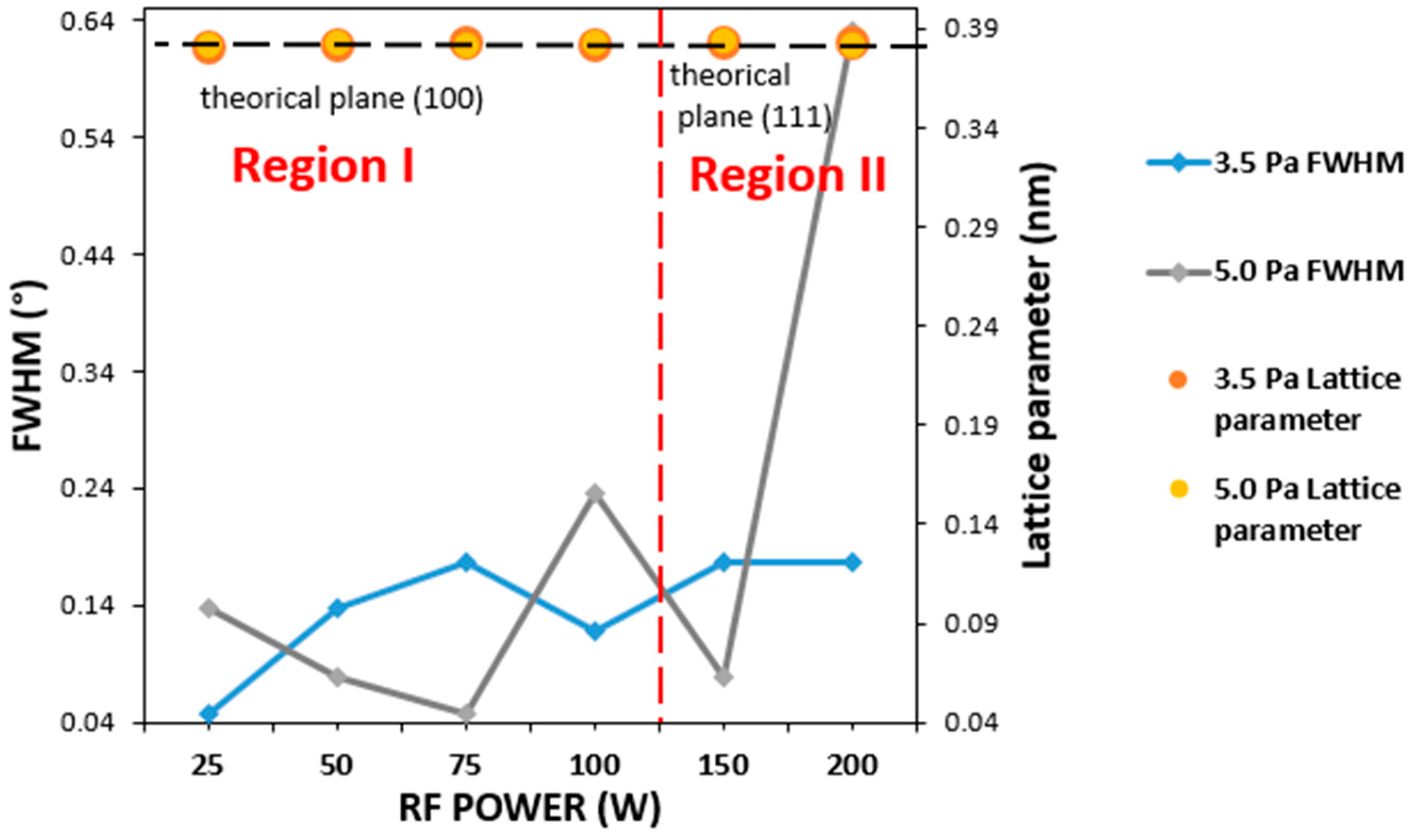
| 2θ (°) | 23.327 | 23.248 | 23.203 | 23.272 | 40.746 | 40.748 |
| Predominant direction | (100) | (100) | (100) | (100) | (111) | (111) |
| Lattice parameter a (nm) | 0.3810 | 0.3826 | 0.3833 | 0.3822 | 0.3836 | 0.3833 |
| FWHM (°) | 0.048 | 0.138 | 0.1771 | 0.1181 | 0.1771 | 0.1771 |
| Grain size (nm) | 30 | 31 | 27 | 36 | 30 | 32 |
| Total Gas Pressure: 5.0 Pa | ||||||
| RF Power (W) | 25 | 50 | 75 | 100 | 150 | 200 |
| 2θ (°) | 23.297 | 23.214 | 23.343 | 23.251 | 40.794 | 23.293 |
| Predominant direction | (100) | (100) | (100) | (100) | (111) | (100) |
| Lattice parameter a (nm) | 0.3818 | 0.3832 | 0.3817 | 0.3826 | 0.3840 | 0.3814 |
| FWHM (°) | 0.1378 | 0.0787 | 0.048 | 0.2362 | 0.0787 | 0.6298 |
| Grain size (nm) | 27 | 36 | 33 | 38 | 27 | 33 |
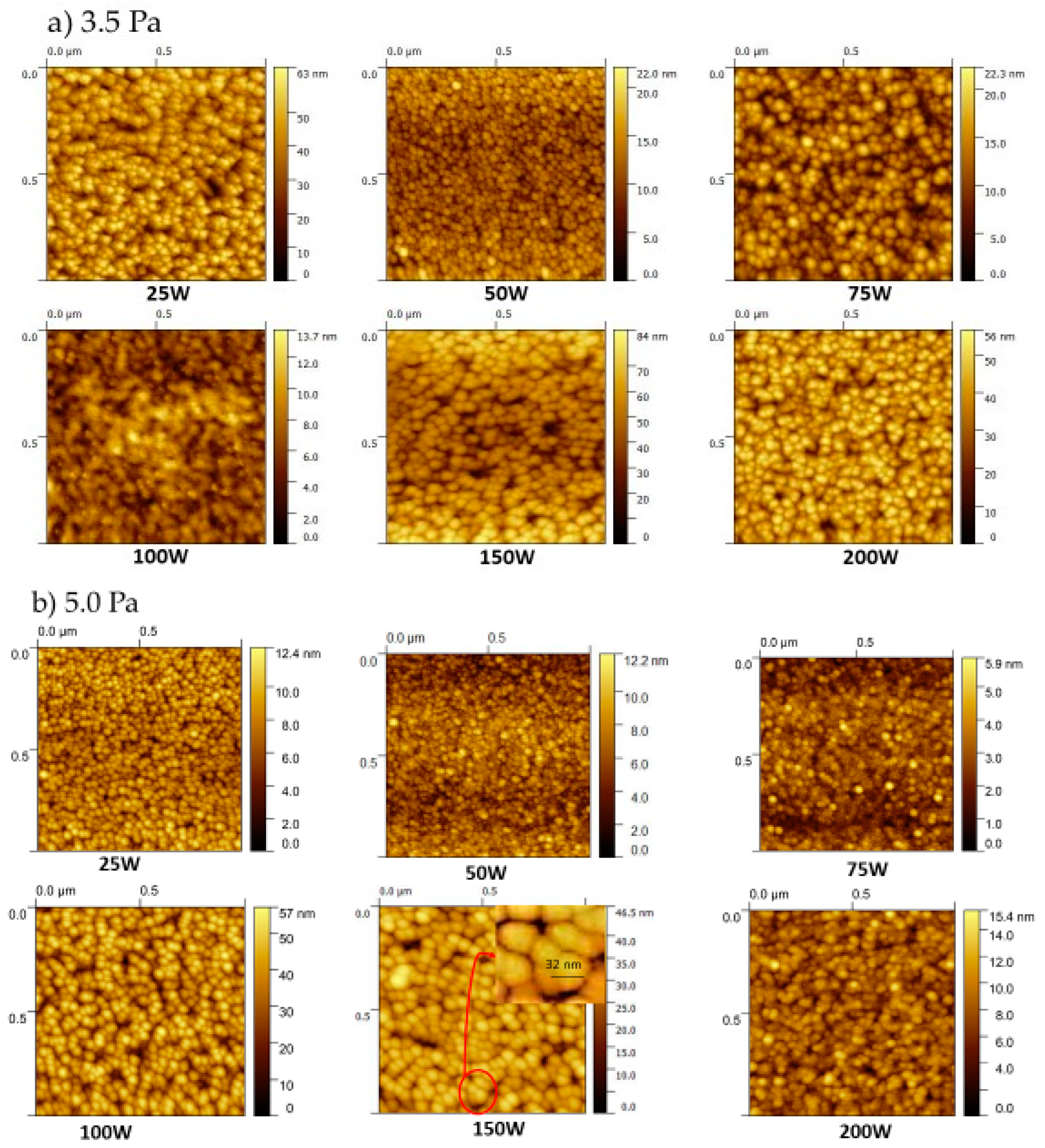
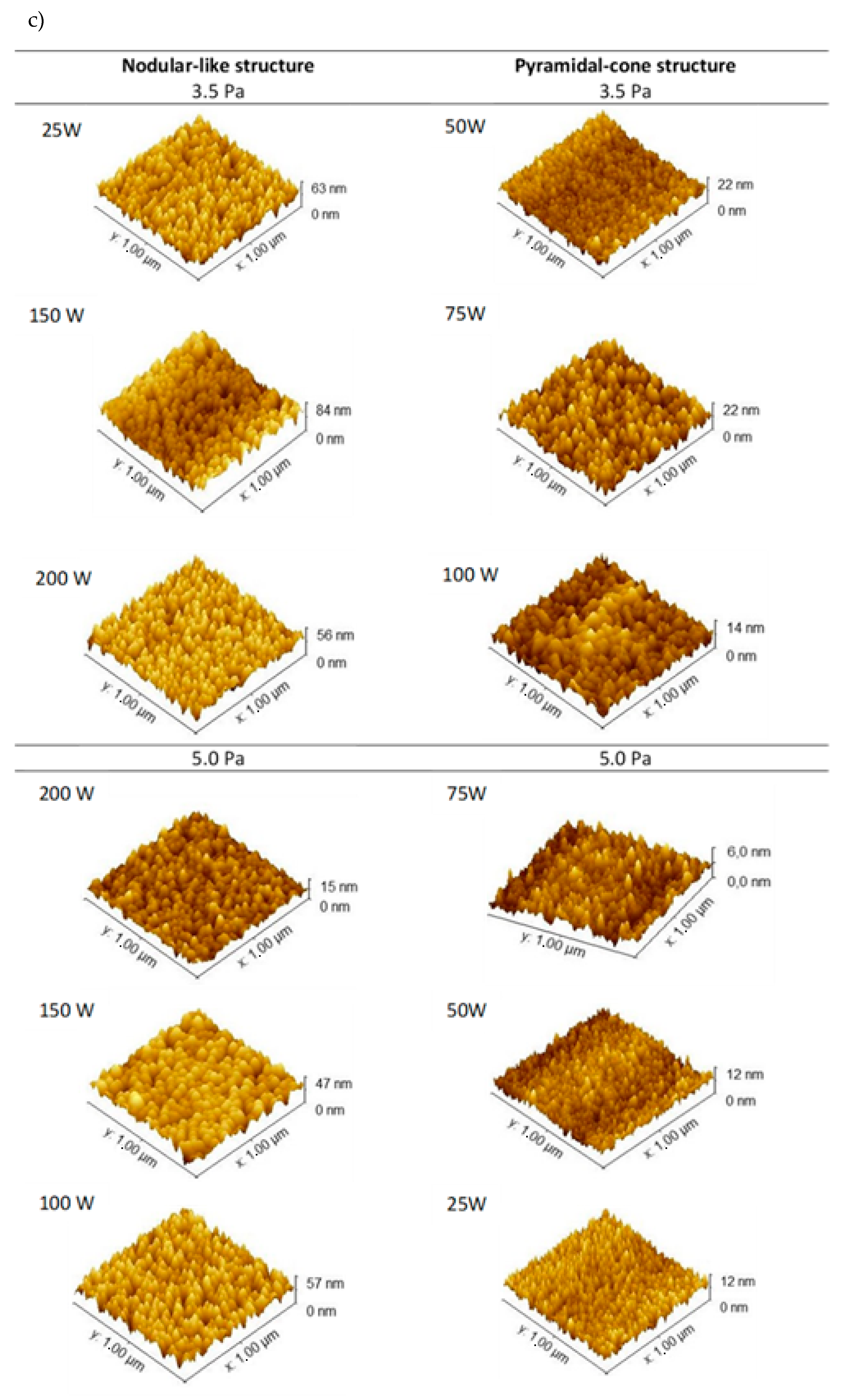
| Total Gas Pressure: 3.5 Pa | ||||||
| RF Power (W) | 25 | 50 | 75 | 100 | 150 | 200 |
| RMS (nm) | 8.50 | 2.20 | 3.25 | 1.77 | 8.81 | 7.40 |
| Grain size (nm) | 31 | 31 | 33 | 34 | 36 | 37 |
| Total Gas Pressure: 5.0 Pa | ||||||
| RF Power (W) | 25 | 50 | 75 | 100 | 150 | 200 |
| RMS (nm) | 1.50 | 1.33 | 1.50 | 8.02 | 5.60 | 5.70 |
| Grain size (nm) | 29 | 35 | 33 | 34 | 32 | 33 |
| RF Power (W) | 25 | 50 | 75 | 100 | 200 |
| Cu/N ratio (3.5 Pa) | 1.85 | 1.94 | 1.70 | 2.15 | 2.33 |
| Cu/N ratio (5.0 Pa) | 1.87 | 2.06 | 2.36 | 2.48 | 2.87 |
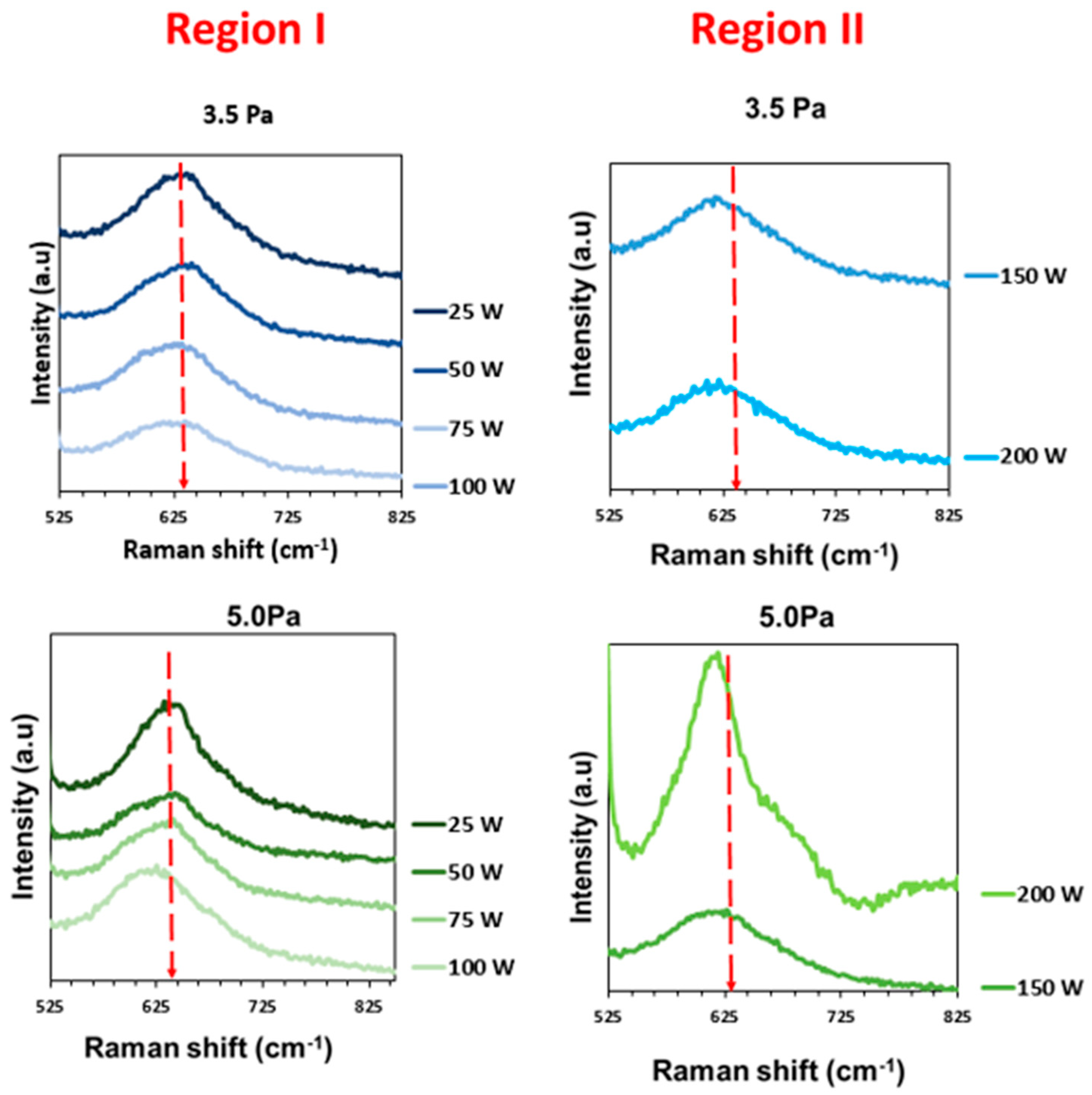
| RF Power (W) | 25 | 50 | 75 | 100 | 150 | 200 |
| FWHM (cm−1) (3.5 Pa) | 66 | 82 | 105 | 99 | 121 | 114 |
| Raman peak (cm−1) | 632 | 637 | 621 | 621 | 616 | 616 |
| FWHM (cm−1) (5.0 Pa) | 108 | 120 | 107 | 118 | 108 | 77 |
| Raman peak (cm−1) | 644 | 640 | 627 | 620 | 616 | 616 |
| Total Gas Pressure: 3.5 Pa | ||||||
| RF Power (W) | 25 | 50 | 75 | 100 | 150 | 200 |
| Eg (eV) | ||||||
| Direct (αhν)2 | 2.30 | 2.10 | 2.05 | 2.05 | 2.00 | 1.90 |
| Indirect (αhν)1/2 | 1.90 | 1.80 | 1.70 | 1.70 | 1.60 | 1.70 |
| Total Gas Pressure: 5.0 Pa | ||||||
| RF Power (W) | 25 | 50 | 75 | 100 | 150 | 200 |
| Eg (eV) | ||||||
| Direct (αhν)2 | 2.10 | 2.18 | 2.05 | 2.01 | 2.05 | 2.10 |
| Indirect (αhν)1/2 | 1.80 | 1.80 | 1.70 | 1.70 | 1.70 | 1.70 |
Disclaimer/Publisher’s Note: The statements, opinions and data contained in all publications are solely those of the individual author(s) and contributor(s) and not of MDPI and/or the editor(s). MDPI and/or the editor(s) disclaim responsibility for any injury to people or property resulting from any ideas, methods, instructions or products referred to in the content. |
© 2023 by the authors. Licensee MDPI, Basel, Switzerland. This article is an open access article distributed under the terms and conditions of the Creative Commons Attribution (CC BY) license (https://creativecommons.org/licenses/by/4.0/).
Share and Cite
Rodríguez-Tapiador, M.I.; Merino, J.; Jawhari, T.; Muñoz-Rosas, A.L.; Bertomeu, J.; Fernández, S. Impact of the RF Power on the Copper Nitride Films Deposited in a Pure Nitrogen Environment for Applications as Eco-Friendly Solar Absorber. Materials 2023, 16, 1508. https://doi.org/10.3390/ma16041508
Rodríguez-Tapiador MI, Merino J, Jawhari T, Muñoz-Rosas AL, Bertomeu J, Fernández S. Impact of the RF Power on the Copper Nitride Films Deposited in a Pure Nitrogen Environment for Applications as Eco-Friendly Solar Absorber. Materials. 2023; 16(4):1508. https://doi.org/10.3390/ma16041508
Chicago/Turabian StyleRodríguez-Tapiador, M. I., J. Merino, T. Jawhari, A. L. Muñoz-Rosas, J. Bertomeu, and S. Fernández. 2023. "Impact of the RF Power on the Copper Nitride Films Deposited in a Pure Nitrogen Environment for Applications as Eco-Friendly Solar Absorber" Materials 16, no. 4: 1508. https://doi.org/10.3390/ma16041508