Application of Nanostructures in Electrochromic Materials and Devices: Recent Progress

Abstract
:1. Introduction
2. Nanostructures in EC Materials and Devices
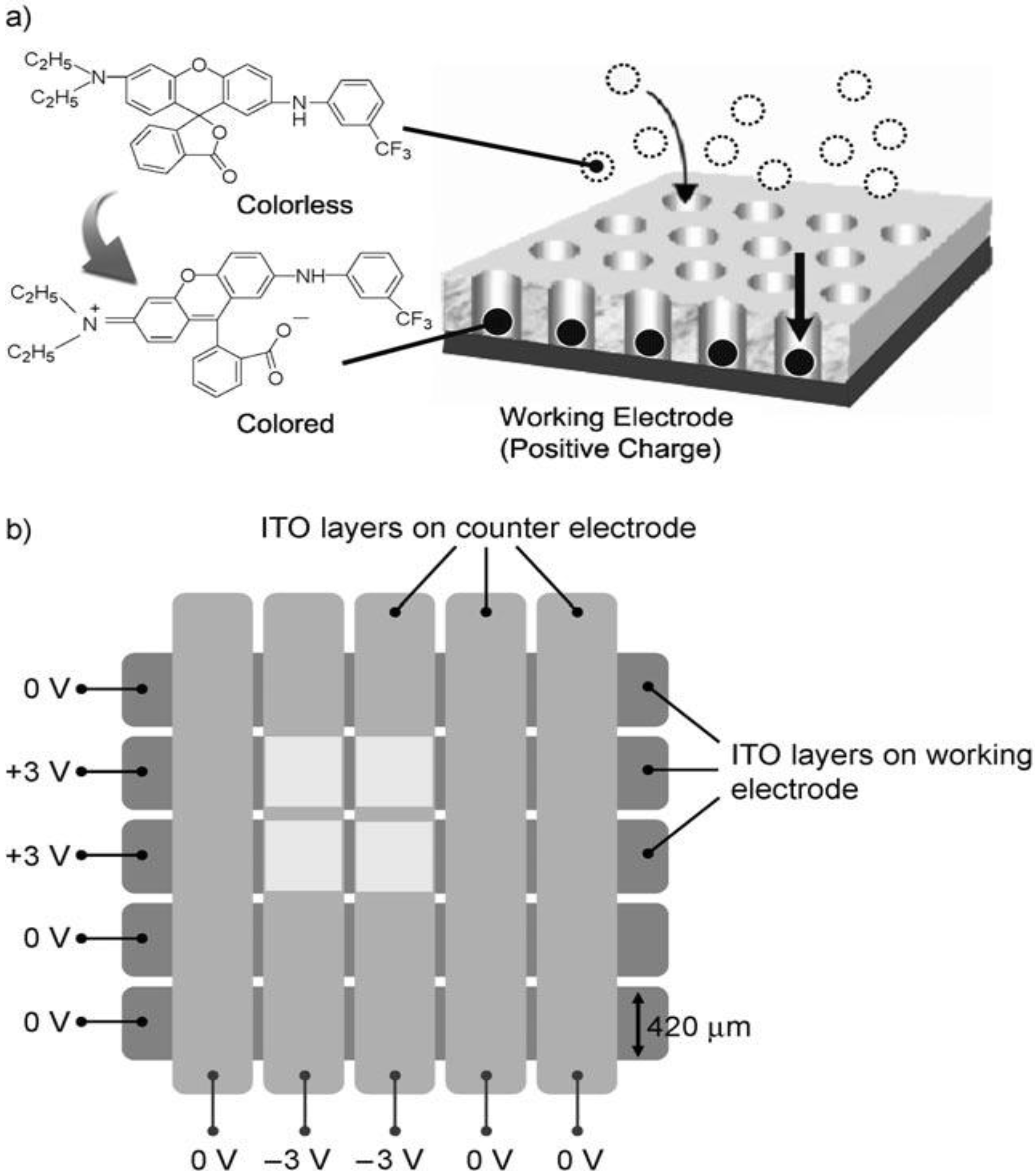
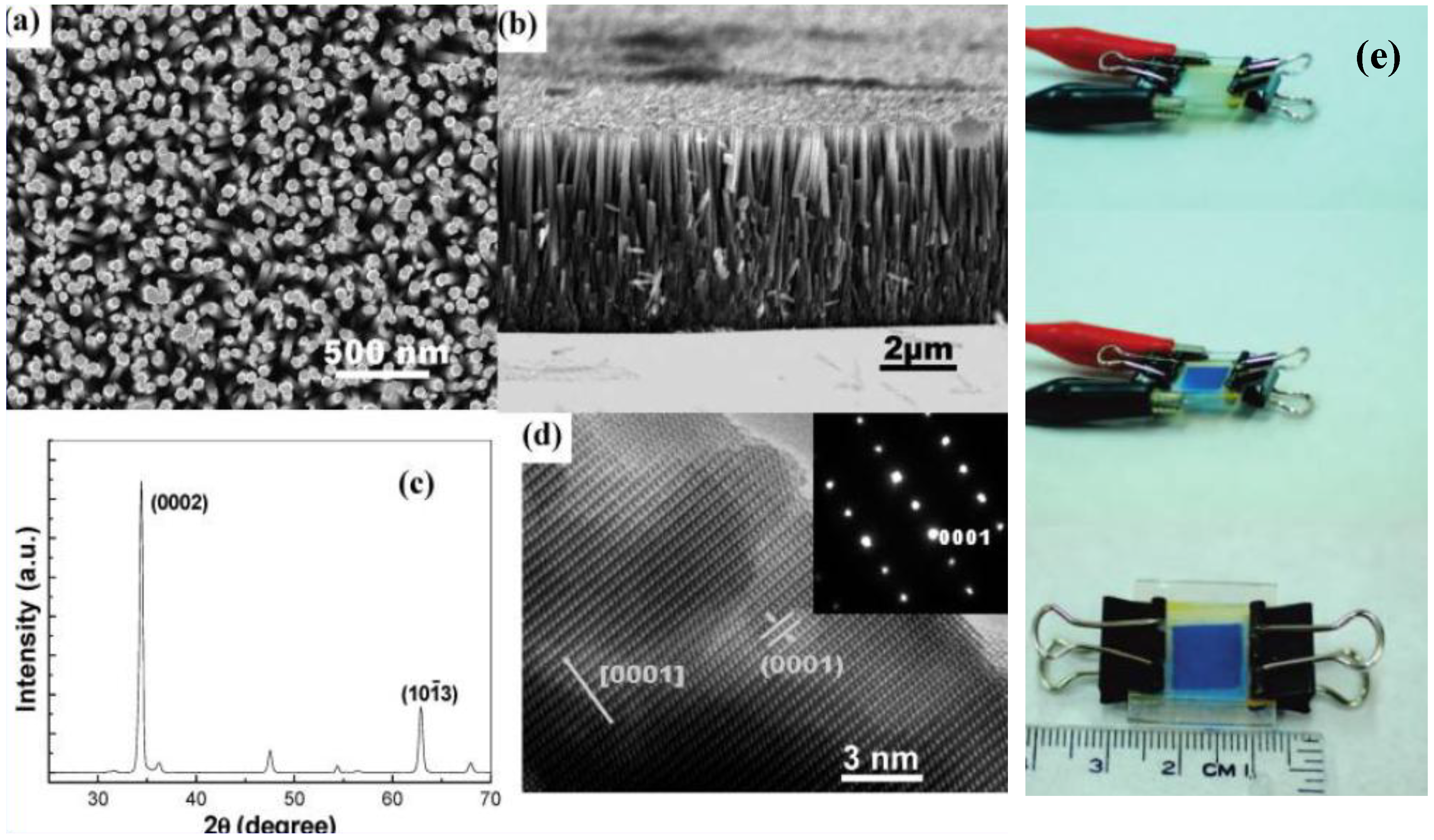
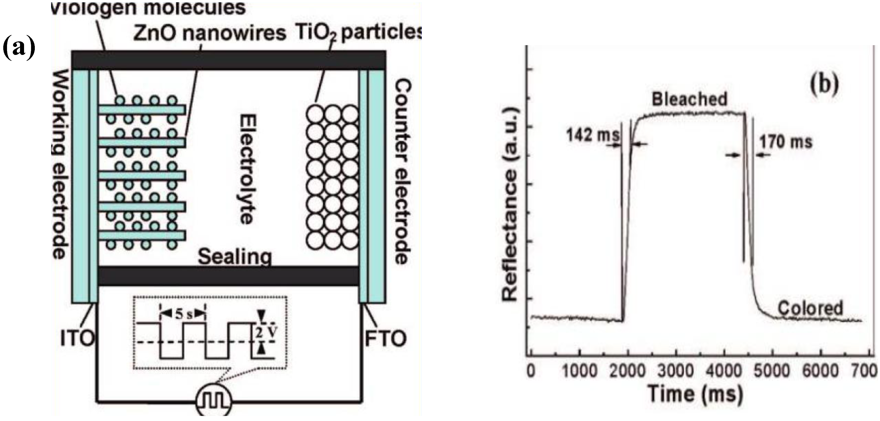
2.1. ZnO Nanowire Array

2.2. Crystalline WO3 Nanostructures


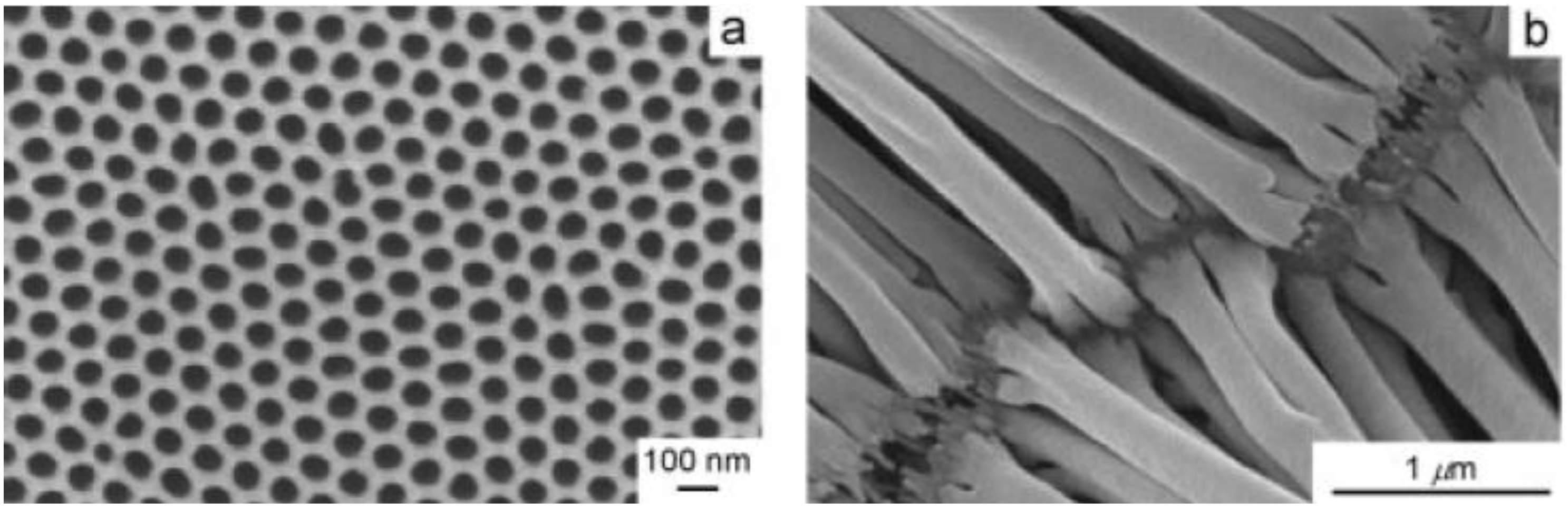
2.3. Mesoporous WO3


2.4. Mesoporous TiO2


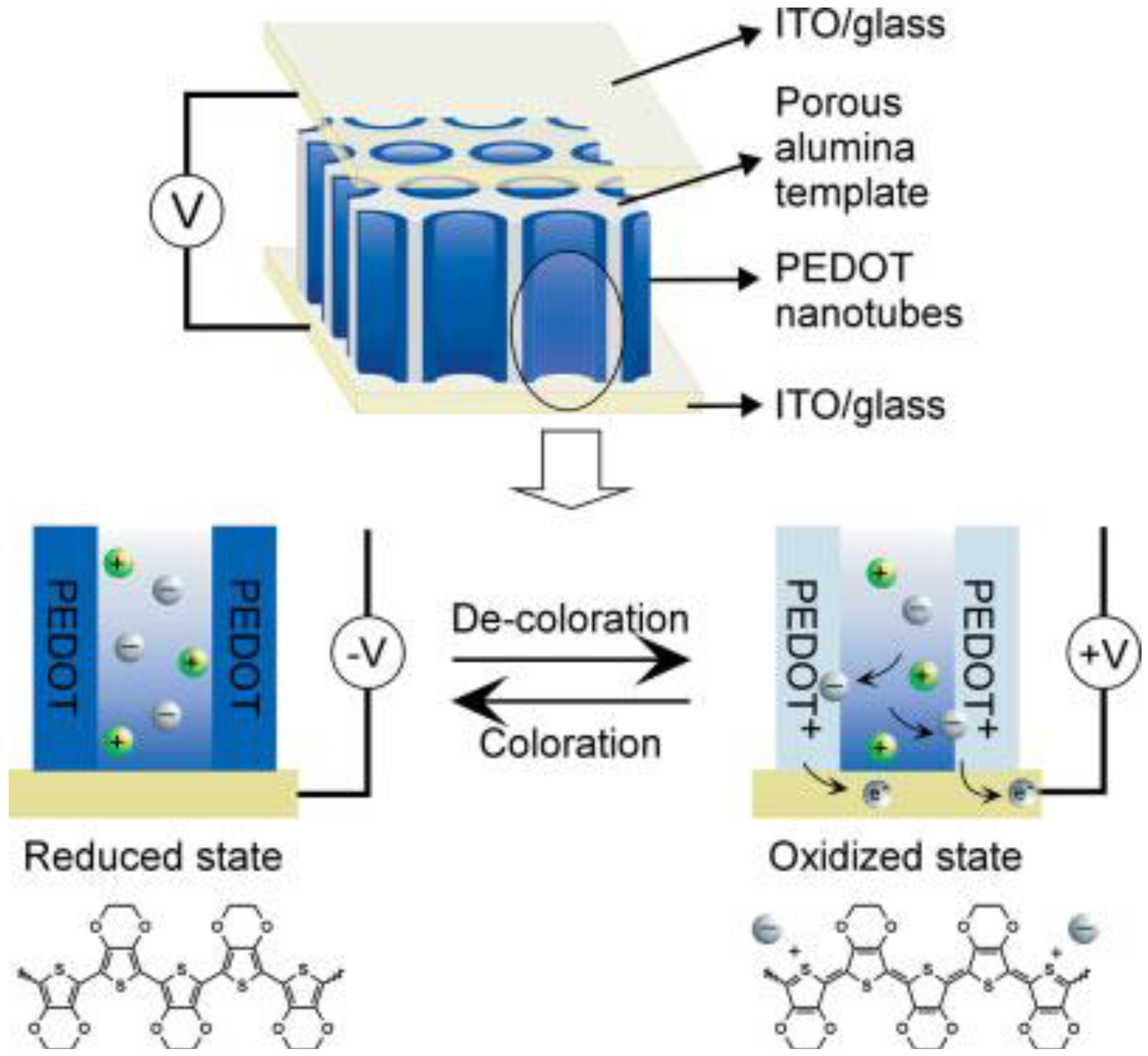
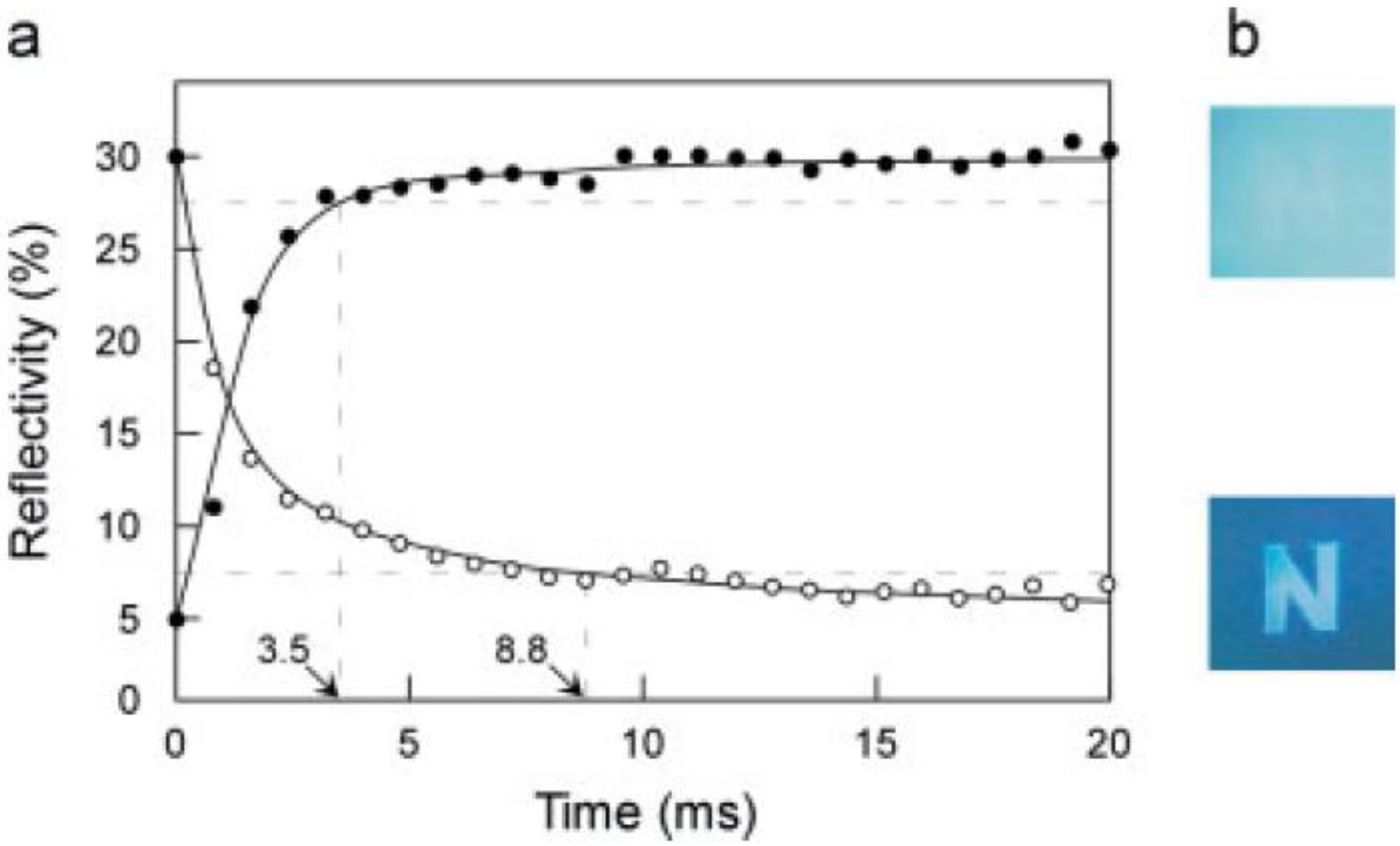
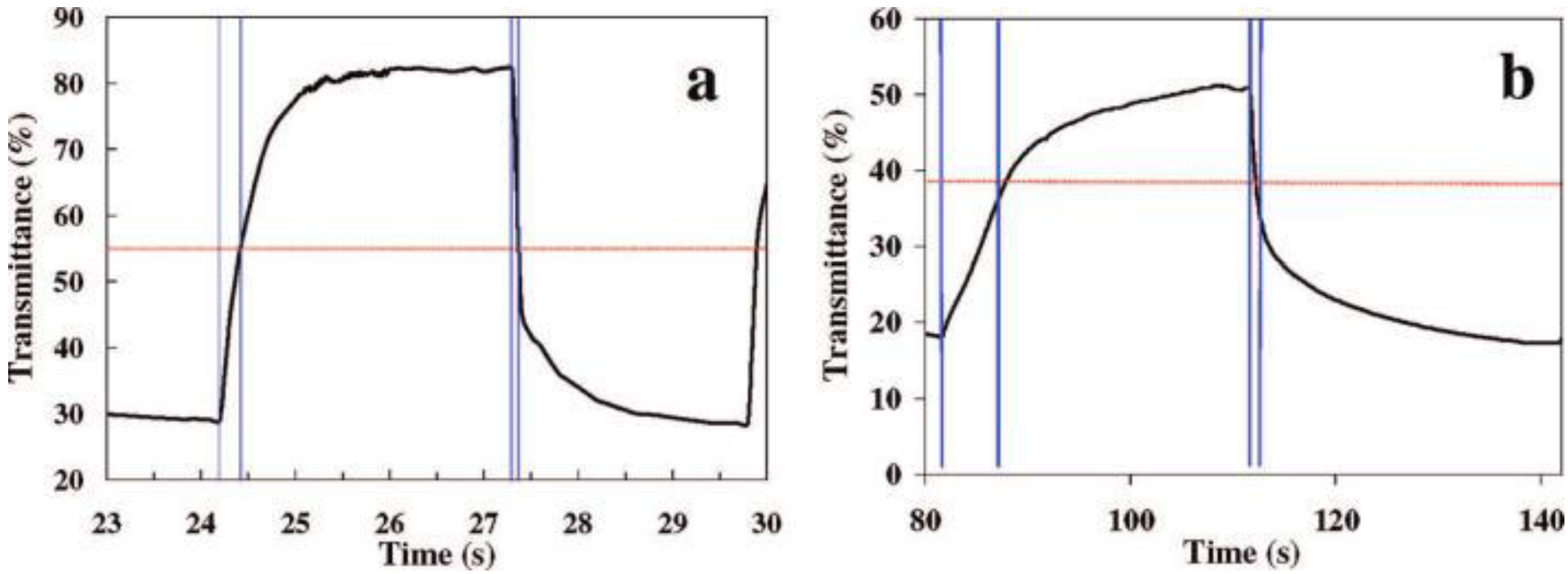
2.5. PEDOT Nanotubes


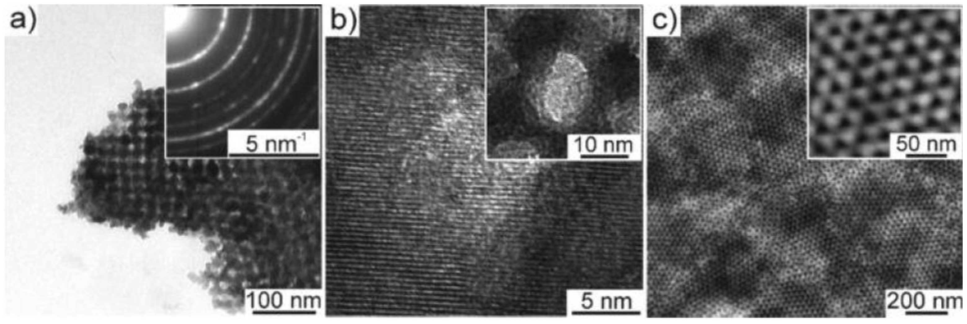
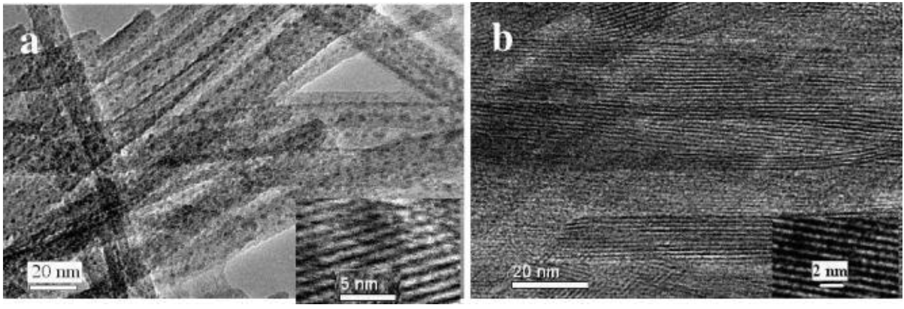
2.6. V2O5 Nanowires
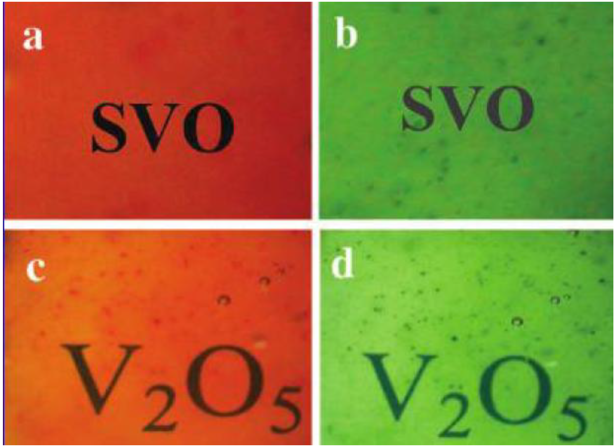

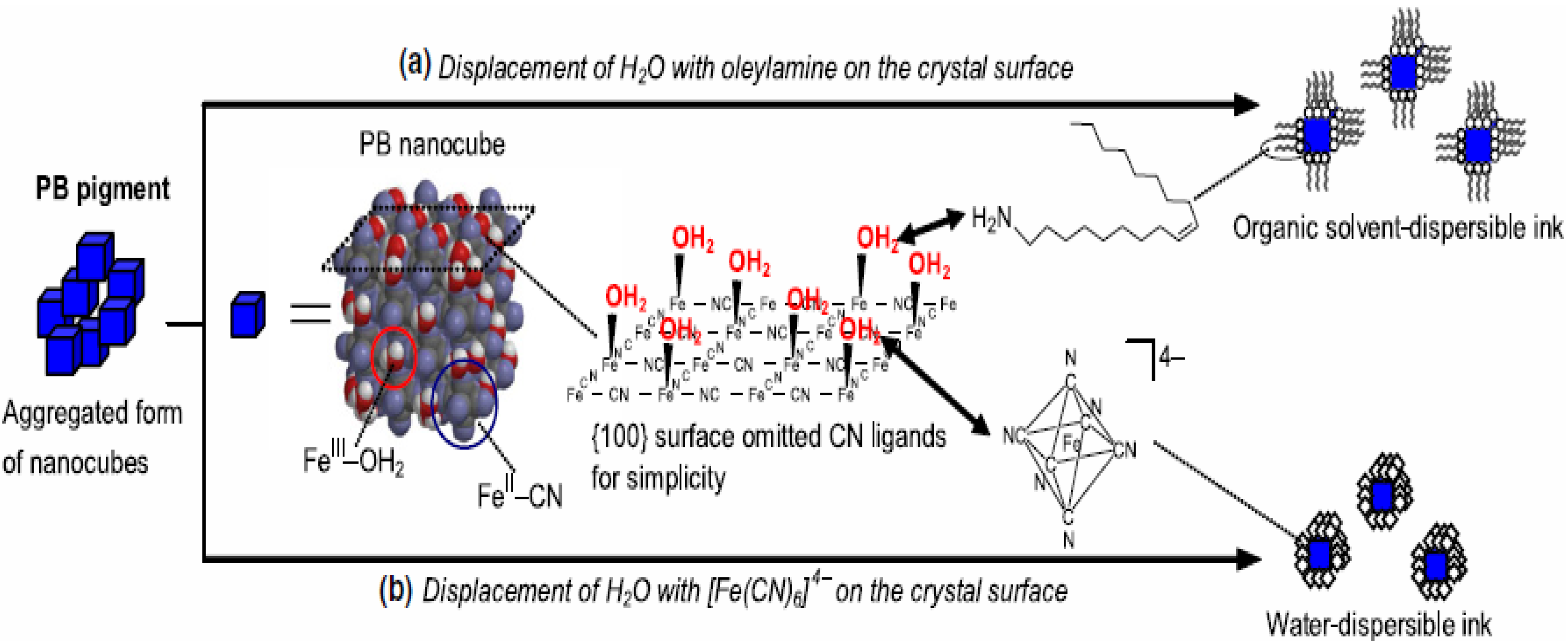
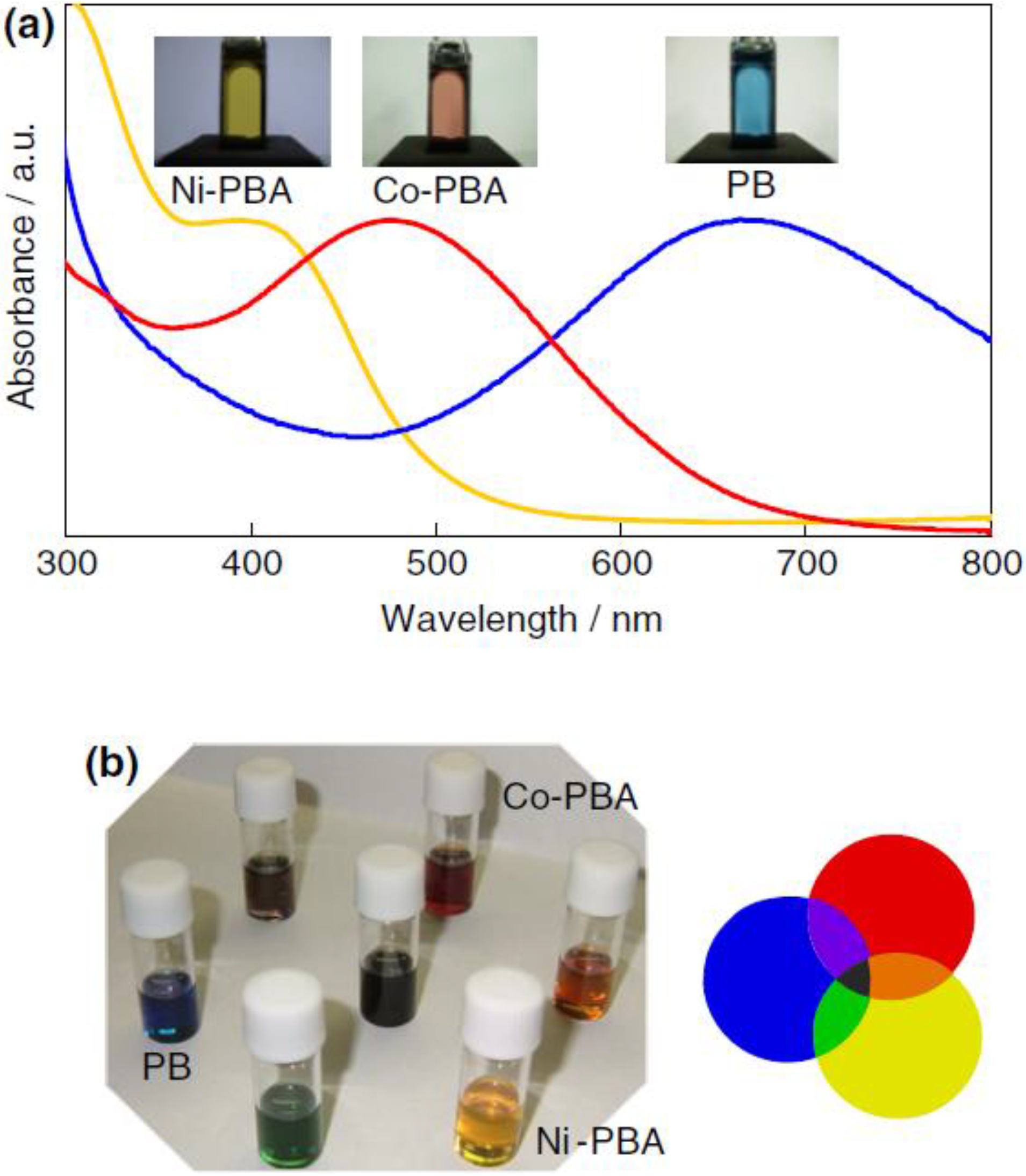
2.7. PB Nanoinks


2.8. Nanostructures in Switchable Mirrors
3. Conclusions and Perspective
Acknowledgements
References
- Granqvist, C.G. Handbook of Inorganic Electrochromic Materials; Elsevier: Amsterdam, The Netherlands, 1995. [Google Scholar]
- Deb, S.K. Reminiscences on the discovery of electrochromic phenomena in transition metal oxides. Solar Energ. Mater. Solar Cells 1995, 39, 191–201. [Google Scholar] [CrossRef]
- Deb, S.K. Opportunities and challenges in science and technology of WO3 for electrochromic and related applications. Solar Energ. Mater. Solar Cells 2008, 92, 245–258. [Google Scholar] [CrossRef]
- Deb, S.K. A novel electrophotographic system. Appl. Opt. Suppl. 1969, 3, 192–195. [Google Scholar]
- Deb, S.K. Optical and photoelectric properties and color centres in thin films of tungsten oxide. Philos. Mag. 1973, 27, 801–822. [Google Scholar] [CrossRef]
- Campus, F.; Bonhôte, P.; Grätzel, M.; Heinen, S.; Walder, L. Electrochromic devices based on surface-modified nanocrystalline TiO2 thin-film electrodes. Solar Energ. Mater. Solar Cells 1999, 56, 281–297. [Google Scholar] [CrossRef]
- Shim, G.H.; Han, M.G.; Sharp-Norton, J.C.; Creagerb, S.E.; Foulger, S.H. Inkjet-printed electrochromic devices utilizing polyaniline-silica and poly(3,4-ethylenedioxythiophene)-silica colloidal composite particles. J. Mater. Chem. 2008, 18, 594–601. [Google Scholar] [CrossRef]
- Liao, C.-C.; Chen, F.-R.; Kai, J.-J. Electrochromic properties of nanocomposite WO3 films. Solar Energ. Mater. Solar Cells 2007, 91, 1282–1288. [Google Scholar]
- Mortimer, R.J.; Dyer, A.L.; Reynolds, J.R. Electrochromic organic and polymeric materials for display applications. Displays 2006, 27, 2–18. [Google Scholar] [CrossRef]
- Granqvist, C.G.; Azensa, A.; Hjelm, A.; Kullman, L.; Niklasson, G.A.; Rönnow, D.; Mattsson, M.S.; Veszelei, M.; Vaivars, G. Recent advances in electrochromics for smart windows applications. Solar Energ. 1998, 63, 199–216. [Google Scholar] [CrossRef]
- Granqvist, C.G. Electrochromic tungsten oxide films: Review of progress 1993-1998. Solar Energ. Mater. Solar Cells 2000, 60, 201–262. [Google Scholar] [CrossRef]
- Baetens, R.; Jelle, B.P.; Gustavsen, A. Properties, requirements and possibilities of smart windows for dynamic daylight and solar energy control in buildings: A state-of-the-art review. Solar Energ. Mater. Solar Cells 2010, 94, 87–105. [Google Scholar] [CrossRef]
- Yoo, S.J.; Lim, J.W.; Sung, Y.-E.; Jung, Y.H.; Choi, H.G.; Kim, D.K. Fast switchable electrochromic properties of tungsten oxide nanowire bundles. Appl. Phys. Lett. 2007, 90, 173126. [Google Scholar] [CrossRef]
- Wu, M.-S.; Yang, C.-H. Electrochromic properties of intercrossing nickel oxide nanoflakes synthesized by electrochemically anodic deposition. Appl. Phys. Lett. 2007, 91, 033109. [Google Scholar] [CrossRef]
- Ghicov, A.; Albu, S.P.; Macak, J.M.; Schmuki, P. High-contrast electrochromic switching using transparent lift-off layers of self-organized TiO2 nanotubes. Small 2008, 4, 1063–1066. [Google Scholar] [CrossRef] [PubMed]
- Cheng, K.-C.; Chen, F.-R.; Kai, J.-J. V2O5 nanowires as a functional material for electrochromic device. Solar Energ. Mater. Solar Cells 2006, 90, 1156–1165. [Google Scholar] [CrossRef]
- Cheng, K.-C.; Chen, F.-R.; Kai, J.-J. Electrochromic property of nano-composite Prussian blue based thin film. Electrochim. Acta 2007, 52, 3330–3335. [Google Scholar] [CrossRef]
- Cinnsealach, R.; Boschloo, G.; Rao, S.N.; Fitzmaurice, D. Electrochromic windows based on viologen-modified nanostructured TiO2 films. Solar Energ. Mater. Solar Cells 1998, 55, 215–223. [Google Scholar] [CrossRef]
- Gospodinova, N.; Terlemezyan, L. Conducting polymers prepared by oxidative polymerization: polyaniline. Prog. Polym. Sci. 1998, 23, 1443–1484. [Google Scholar] [CrossRef]
- Andersson, P.; Forchheimer, R.; Tehrani, P.; Berggren, M. Printable all-organic electrochromic active-matrix displays. Adv. Funct. Mater. 2007, 17, 3074–3082. [Google Scholar] [CrossRef]
- Niklasson, G.A.; Granqvist, C.G. Electrochromics for smart windows: thin films of tungsten oxide and nickel oxide, and devices based on these. J. Mater. Chem. 2007, 17, 127–156. [Google Scholar] [CrossRef]
- Avendaño, E.; Berggren, L.; Niklasson, G.A.; Granqvist, C.G.; Azens, A. Electrochromic materials and devices: Brief survey and new data on optical absorption in tungsten oxide and nickel oxide films. Thin Solid Films 2006, 496, 30–36. [Google Scholar] [CrossRef]
- Dautremont-Smith, W.C.; Beni, G.; Schiavone, L.M.; Shay, J.L. Solid-state electrochromic cell with anodic iridium oxide film electrodes. Appl. Phys. Lett. 1979, 35, 565. [Google Scholar] [CrossRef]
- Patila, P.S.; Kawarb, R.K.; Sadale, S.B. Electrochromism in spray deposited iridium oxide thin films. Electrochim. Acta 2005, 50, 2527–2532. [Google Scholar] [CrossRef]
- DeLongchamp, D.M.; Hammond, P.T. High-contrast electrochromism and controllable dissolution of assembled Prussian blue/polymer nanocomposites. Adv. Funct. Mater. 2004, 14, 224–232. [Google Scholar] [CrossRef]
- Granqvist, C.G. Solar energy materials. Adv. Mater. 2003, 15, 1789–1803. [Google Scholar] [CrossRef]
- Granqvist, C.G.; Avendaño, E.; Azens, A. Electrochromic coatings and devices: survey of some recent advances. Thin Solid Films 2003, 442, 201–211. [Google Scholar] [CrossRef]
- Granqvist, C.G.; Azens, A.; Heszler, P.; Kish, L.B.; Osterlund, L. Nanomaterials for benign indoor environments: Electrochromics for “smart windows”, sensors for air quality, and photo-catalysts for air cleaning. Solar Energ. Mater. Solar Cells 2007, 91, 355–365. [Google Scholar] [CrossRef]
- Granqvist, C.G. Oxide electrochromics: Why, how, and whither. Solar Energ. Mater. Solar Cells 2008, 92, 203–208. [Google Scholar] [CrossRef]
- Granqvist, C.G.; Lansaker, P.C.; Mlyuka, N.R.; Niklasson, G.A.; Avendaño, E. Progress in chromogenics: New results for electrochromic and thermochromic materials and devices. Solar Energ. Mater. Solar Cells 2009, 93, 2032–2039. [Google Scholar] [CrossRef]
- Granqvist, C.G.; Green, S.; Niklasson, G.A.; Mlyuka, N.R.; von Kræmer, S.; Georén, P. Advances in chromogenic materials and devices. Thin Solid Films 2010, 518, 3046–3053. [Google Scholar] [CrossRef]
- Vayssieres, L. Growth of arrayed nanorods and nanowires of ZnO from aqueous solutions. Adv. Mater. 2003, 15, 464–466. [Google Scholar] [CrossRef]
- Sun, X.W.; Wang, J.X. Fast switching electrochromic display using a viologen-modified ZnO nanowire array electrode. Nano Lett. 2008, 8, 1884–1889. [Google Scholar] [CrossRef]
- Wang, M.J.; Fang, G.J.; Yuan, L.Y.; Huang, H.H.; Sun, Z.H.; Liu, N.S.; Xia, S.H.; Zhao, X.Z. High optical switching speed and flexible electrochromic display based on WO3 nanoparticles with ZnO nanorod arrays’ supported electrode. Nanotechnology 2009, 20, 185304. [Google Scholar] [CrossRef] [PubMed]
- Deepa, M.; Joshi, A.G.; Srivastava, A.K.; Shivaprasad, S.M.; Agnihotry, S.A. Electrochromic nanostructured tungsten oxide films by sol-gel: Structure and intercalation properties. J. Electrochem. Soc. 2006, 153, C365–C376. [Google Scholar] [CrossRef]
- Deepa, M.; Saxena, T.K.; Singh, D.P.; Sood, K.N.; Agnihotry, S.A. Spin coated versus dip coated electrochromic tungsten oxide films: Structure, morphology, optical and electrochemical properties. Electrochim. Acta 2006, 51, 1974–1989. [Google Scholar] [CrossRef]
- Subrahmanyam, A.; Karuppasamy, A. Optical and electrochromic properties of oxygen sputtered tungsten oxide (WO3) thin films. Solar Energ. Mater. Solar Cells 2007, 91, 266–274. [Google Scholar] [CrossRef]
- Lee, S.-H.; Deshpande, R.; Parilla, P.A.; Jones, K.M.; To, B.; Mahan, A.H.; Dillon, A.C. Crystalline WO3 nanoparticles for highly improved electrochromic applications. Adv. Mater. 2006, 18, 763–766. [Google Scholar] [CrossRef]
- Wang, J.M.; Khoo, E.; Lee, P.S.; Ma, J. Synthesis, assembly and electrochromic properties of uniform crystalline WO3 nanorods. J. Phys. Chem. C 2008, 112, 14306–14312. [Google Scholar] [CrossRef]
- Wang, J.M.; Khoo, E.; Lee, P.S.; Ma, J. Controlled synthesis of WO3 nanorods and their electrochromic properties in H2SO4 electrolyte. J. Phys. Chem. C 2009, 113, 9655–9658. [Google Scholar] [CrossRef]
- Jiao, Z.H.; Sun, X.W.; Wang, J.M.; Ke, L.; Demir, H.V. Hydrothermally grown nanostructured WO3 films and their electrochromic characteristics. J. Phys. D: Appl. Phys. 2010, 43, 285501. [Google Scholar] [CrossRef]
- Baeck, S.-H.; Choi, K.-S.; Jaramillo, T.E.; Stucky, G.D.; McFarland, E.W. Enhancement of photocatalytic and electrochromic properties of electrochemically fabricated mesoporous WO3 thin films. Adv. Mater. 2003, 15, 1269–1273. [Google Scholar] [CrossRef]
- Brezesinski, T.; Fattakhova-Rohlfing, D.; Sallard, S.; Antonietti, M.; Smarsly, B.M. Highly crystalline WO3 thin films with ordered 3D mesoporosity and improved electrochromic performance. Small 2006, 10, 1203–1211. [Google Scholar] [CrossRef]
- Sallard, S.; Brezesinski, T.; Smarsly, B.M. Electrochromic stability of WO3 thin films with nanometer-scale periodicity and varying degrees of crystallinity. J. Phys. Chem. C 2007, 111, 7200–7206. [Google Scholar] [CrossRef]
- Cinnsealach, R.; Boschloo, G.; Nagaraja, R.S.; Fitzmaurice, D. Solar Energ. Mater. Solar Cells 1999, 57, 107–125. [CrossRef]
- Bonhote, P.; Gogniat, E.; Gratzel, M.; Ashrit, P.V. Novel electrochromic devices based on complementary nanocrystalline TiO2 and WO3 thin films. Thin Solid Films 1999, 350, 269–275. [Google Scholar] [CrossRef]
- Campus, F.; Bonhote, P.; Gratzel, M.; Heinen, S.; Walder, L. Electrochromic devices based on surface-modified nanocrystalline TiO2 thin-film electrodes. Solar Energ. Mater. Solar Cells 1999, 56, 281–297. [Google Scholar] [CrossRef]
- Cummins, D.; Boschloo, G.; Ryan, M.; Corr, D.; Nagaraja, R.S.; Fitzmaurice, D. Ultrafast electrochromic windows based on redox-chromophore modified nanostructured semiconducting and conducting films. J. Phys. Chem. B 2000, 104, 11449–11459. [Google Scholar] [CrossRef]
- Bach, U.; Corr, D.; Lupo, D.; Pichot, F.; Ryan, M. Nanomaterials-based electrochromics for paper-quality displays. Adv. Mater. 2002, 14, 845–848. [Google Scholar] [CrossRef]
- Choi, S.Y.; Mamak, M.; Coombs, N.; Chopra, N.; Ozin, G.A. Electrochromic performance of viologen-modified periodic mesoporous nanocrystalline anatase electrodes. Nano Lett. 2004, 4, 1231–1235. [Google Scholar] [CrossRef]
- Weng, W.; Higuchi, T.; Suzuki, M.; Fukuoka, T.; Shimomura, T.; Ono, M.; Radhakrishnan, L.; Wang, H.; Suzuki, N.; Hamid, O.; Yamauchi, Y. A high-speed passive-matrix electrochromic display using a mesoporous TiO2 electrode with vertical porosity. Angew. Chem. Int. Ed. 2010, 49, 3956–3959. [Google Scholar] [CrossRef]
- Cho, C.I.; Kwon, W.J.; Choi, S.-J.; Kim, P.; Park, S.-A.; Kim, J.; Son, S.J.; Xiao, R.; Kim, S.-H.; Lee, S.B. Nanotube-based ultrafast electrochromic display. Adv. Mater. 2005, 17, 171–175. [Google Scholar] [CrossRef]
- Xiong, C.; Aliev, A.E.; Gnade, B.; Balkus, K.J., Jr. Fabrication of silver vanadium oxide and V2O5 nanowires for electrochromics. ACS Nano 2008, 2, 293–301. [Google Scholar] [CrossRef] [PubMed]
- Brown, J. Observations and experiments upon the foregoing preparation. Philos. Trans. 1724, 33, 17–24. [Google Scholar] [CrossRef]
- Sharpe, A.G. The Chemistry of Cysno Complexes of the Transition Metals; Academic Press: New York, NY, USA, 1976. [Google Scholar]
- Neff, V.D. Electrochemical oxidation and reduction of thin-films of Prussian blue. J. Electrochem. Soc. 1978, 125, 886–887. [Google Scholar] [CrossRef]
- Ellis, D.; Eckhoff, M.; Neff, V.D. Electrochromism in the mixed-valence hexacyanides. 1. Voltammetric and spectral studies of the oxidation and reduction of thin-films of Prussian blue. J. Phys. Chem. 1981, 85, 1225–1231. [Google Scholar] [CrossRef]
- Itaya, K.; Shibayama, K.; Akahoshi, H.; Toshima, S. Prussian-blue-modified electrodes: An application for stable electrochromic display device. J. Appl. Phys. 1982, 53, 804–805. [Google Scholar] [CrossRef]
- Itaya, K.; Ataka, T.; Toshima, S. Spectroelectrochemistry and electrochemical preparation method of Prussian blue modified electrodes. J. Am. Chem. Soc. 1982, 104, 4767–4772. [Google Scholar] [CrossRef]
- Itaya, K.; Uchida, I.; Neff, V.D. Electrochemistry of polynuclear transition-metal cyanides-Prussian blue and its analogs. Accounts Chem. Res. 1986, 19, 162–168. [Google Scholar] [CrossRef]
- Rajan, K. P.; Neff, V.D. Electrochromism in the mixed-valence hexacyanides. 2. Kinetics of the reduction of ruthenium purple and Prussian blue. J. Phys. Chem. 1982, 86, 4361–4368. [Google Scholar] [CrossRef]
- Garjonyte, R.; Malinauskas, A. Operational stability of amperometric hydrogen peroxide sensors, based on ferrous and copper hexacyanoferrates. Sensor Actuator. B-Chem. 1999, 56, 93–97. [Google Scholar] [CrossRef]
- Karyakin, A.A.; Gitelmacher, O.V.; Karyakina, E.E. Prussian blue based first-generation biosensor—A sensitive amperometric electrode for glucose. Anal. Chem. 1995, 67, 2419–2423. [Google Scholar] [CrossRef]
- Karyakin, A.A.; Puganova, E.A.; Budashov, I.A.; Kurochkin, I.N.; Karyakina, E.E.; Levchenko, V.A.; Matveyenko, V.N.; Varfolomeyev, S.D. Prussian blue based nanoelectrode arrays for H2O2 detection. Anal. Chem. 2004, 76, 474–478. [Google Scholar] [CrossRef] [PubMed]
- Mortimer, R.J.; Rosseinsky, D.R. Iron Hexacyanoferrate films-spectroelectrochemical distinction and electrodeposition sequence of soluble (K+-containing) and insoluble (K+-free) Prussian blue, and composition changes in polyelectrochromic switching. J. Chem. Soc., Dalton Trans. 1984, 2059–2061. [Google Scholar]
- Hamnett, A.; Higgins, S.; Mortimer, R.S.; Rosseinsky, D.R. A study of the electrodeposition and subsequent potential cycling of Prussian blue films using ellipsometry. J. Electroanal. Chem. 1988, 255, 315–324. [Google Scholar] [CrossRef]
- Karyakin, A.A.; Karyakina, E.E.; Gorton, L. Prussian-blue-based amperometric biosensors in flow-injection analysis. Talanta 1996, 43, 1597–1606. [Google Scholar] [CrossRef] [PubMed]
- Mortimer, R.J. Electrochromic materials. Chem. Soc. Rev. 1997, 26, 147–156. [Google Scholar] [CrossRef]
- Somani, P.R.; Radhakrishnan, S. Electrochromic materials and devices: present and future. Mater. Chem. Phys. 2003, 77, 117–133. [Google Scholar] [CrossRef]
- Gotoh, A.; Uchida, H.; Ishizaki, M.; Satoh, T.; Kaga, S.; Okamoto, S.; Ohta, M.; Sakamoto, M.; Kawamoto, T.; Tanaka, H.; Tokumoto, M.; Hara, S.; Shiozaki, H.; Yamada, M.; Miyake, M.; Kurihara, M. Simple synthesis of three primary colour nanoparticle inks of Prussian blue and its analogues. Nanotechnology 2007, 18, 345609. [Google Scholar] [CrossRef]
- Hara, S.; Tanaka, H.; Kawamoto, T.; Tokumoto, M.; Yamada, M.; Gotoh, A.; Uchida, H.; Kurihara, M.; Sakamoto, M. Electrochromic thin film of Prussian blue nanoparticles fabricated using wet process. Jpn. J. Appl. Phys. Pt 2 2007, 46, L945–L947. [Google Scholar] [CrossRef]
- Hara, S.; Shiozaki, H.; Omura, A.; Tanaka, H.; Kawamoto, T.; Tokumoto, M.; Yamada, M.; Gotoh, A.; Kurihara, M.; Sakamoto, M. Color-switchable glass and display devices fabricated by liquid processes with electrochromic nanoparticle “ink”. Appl. Phys. Express 2008, 1, 104002. [Google Scholar] [CrossRef]
- Shiozaki, H.; Kawamoto, T.; Tanaka, H.; Hara, S.; Tokumoto, M.; Gotoh, A.; Satoh, T.; Ishizaki, M.; Kurihara, M.; Sakamoto, M. Electrochromic thin film fabricated using a water-dispersible ink of Prussian blue nanoparticles. Jpn. J. Appl. Phys. 2008, 47, 1242–1244. [Google Scholar] [CrossRef]
- Omura, A.; Tanaka, H.; Kurihara, M.; Sakamoto, M.; Kawamoto, T. Electrochemical control of the elution property of Prussian blue nanoparticle thin films: Mechanism and applications. Phys. Chem. Chem. Phys. 2009, 11, 10500–10505. [Google Scholar] [CrossRef] [PubMed]
- Richardson, T.J.; Slack, J.L.; Armitage, R.D.; Kostecki, R.; Farangis, B.; Rubin, M.D. Switchable mirrors based on nickel-magnesium films. Appl. Phys. Lett. 2001, 78, 3047–3049. [Google Scholar] [CrossRef]
- Farangis, B.; Nachimuthu, P.; Richardson, T.J.; Slack, J.L.; Perera, R.C.C.; Gullikson, E.M.; Lindle, D.W.; Rubin, M. In situ x-ray-absorption spectroscopy study of hydrogen absorption by nickel-magnesium thin films. Phys. Rev. B 2003, 67, 085106. [Google Scholar] [CrossRef]
- Lohstroh, W.; Westerwaal, R.J.; van Mechelen, J.L.M.; Chacon, C.; Johansson, E.; Dam, B.; Griessen, R. Structural and optical properties of Mg2NiHx switchable mirrors upon hydrogen loading. Phys. Rev. B 2004, 70, 165411. [Google Scholar] [CrossRef]
- Borsa, D.M.; Gremaud, R.; Baldi, A.; Schreuders, H.; Rector, J.H.; Kooi, B.; Vermeulen, P.; Notten, P.H.L.; Dam, B.; Griessen, R. Structural, optical, and electrical properties of MgyTi1-yHx thin films. Phys. Rev. B 2007, 75, 205408. [Google Scholar] [CrossRef]
- Bao, S.; Tajima, K.; Yamada, Y.; Okada, M.; Yoshimura, K. Magnesium-titanium alloy thin-film switchable mirrors. Solar Energ. Mater. Solar Cells 2008, 92, 224–227. [Google Scholar] [CrossRef]
- Huiberts, J.N.; Griessen, R.; Rector, J.H.; Wijngaargen, R.J.; Dekker, J.P.; de Groot, D.G.; Koeman, N.J. Yttrium and lanthanum hydride films with switchable optical properties. Nature 1996, 380, 231–234. [Google Scholar] [CrossRef]
- van der Sluis, P.; Ouwerkerk, M.; Duine, P.A. Optical switches based on magnesium lanthanide alloy hydrides. Appl. Phys. Lett. 1997, 70, 3356–3358. [Google Scholar] [CrossRef]
- Yoshimura, K.; Yamada, Y.; Okada, M. Optical switching of Mg-rich Mg-Ni alloy thin films. Appl. Phys. Lett. 2002, 81, 4709–4711. [Google Scholar] [CrossRef]
- Yoshimura, K.; Bao, S.H.; Yamada, Y.; Okada, M. Optical switching property of Pd-capped Mg-Ni alloy thin films prepared by magnetron sputtering. Vacuum 2006, 80, 684–687. [Google Scholar] [CrossRef]
- Bao, S.; Tajima, K.; Yamada, Y.; Okada, M.; Yoshimura, K. Color-neutral switchable mirrors based on magnesium-titanium thin films. Appl. Phys. A: Mater. 2007, 87, 621–624. [Google Scholar] [CrossRef]
- Griessen, R.; Huiberts, J.N.; Kremers, M.; van Gogh, A.T.M.; Koeman, N.J.; Dekker, J.P.; Notten, P.H.L. Yttrium and lanthanum hydride films with switchable optical properties. J. Alloy. Compd. 1997, 253-254, 44–50. [Google Scholar] [CrossRef]
- Richardson, T.J.; Slack, J.L.; Armitage, R.D.; Kostecki, R.; Farangis, B.; Rubin, M.D. Switchable mirrors based on nickel-magnesium films. Appl. Phys. Lett. 2001, 78, 3047–3049. [Google Scholar] [CrossRef]
- Yamada, Y.; Bao, S.; Tajima, K.; Okada, M.; Yoshimura, K. Optical properties of switchable mirrors based on magnesium-calcium alloy thin films. Appl. Phys. Lett. 2009, 94, 191910. [Google Scholar] [CrossRef]
- Richardson, T.J. New electrochromic mirror systems. Solid State Ionics 2003, 165, 305–308. [Google Scholar] [CrossRef]
- Liu, G.; Richardson, T.J. Sb-Cu-Li electrochromic mirrors. Solar Energ. Mater. Solar Cells 2005, 86, 113–121. [Google Scholar] [CrossRef]
© 2010 by the authors; licensee MDPI, Basel, Switzerland. This article is an open access article distributed under the terms and conditions of the Creative Commons Attribution license (http://creativecommons.org/licenses/by/3.0/).
Share and Cite
Wang, J.M.; Sun, X.W.; Jiao, Z. Application of Nanostructures in Electrochromic Materials and Devices: Recent Progress. Materials 2010, 3, 5029-5053. https://doi.org/10.3390/ma3125029
Wang JM, Sun XW, Jiao Z. Application of Nanostructures in Electrochromic Materials and Devices: Recent Progress. Materials. 2010; 3(12):5029-5053. https://doi.org/10.3390/ma3125029
Chicago/Turabian StyleWang, Jin Min, Xiao Wei Sun, and Zhihui Jiao. 2010. "Application of Nanostructures in Electrochromic Materials and Devices: Recent Progress" Materials 3, no. 12: 5029-5053. https://doi.org/10.3390/ma3125029