Study of Direct-Contact HfO2/Si Interfaces

National Institute of Advanced Industrial Science and Technology (AIST), Tsukuba, Ibaraki 305-8562, Japan
Materials 2012, 5(3), 512-527; https://doi.org/10.3390/ma5030512
Submission received: 27 February 2012
/
Revised: 5 March 2012
/
Accepted: 8 March 2012
/
Published: 19 March 2012
(This article belongs to the Special Issue High-k Materials and Devices)
Abstract
:Controlling monolayer Si oxide at the HfO2/Si interface is a challenging issue in scaling the equivalent oxide thickness of HfO2/Si gate stack structures. A concept that the author proposes to control the Si oxide interface by using ultra-high vacuum electron-beam HfO2 deposition is described in this review paper, which enables the so-called direct-contact HfO2/Si structures to be prepared. The electrical characteristics of the HfO2/Si metal-oxide-semiconductor capacitors are reviewed, which suggest a sufficiently low interface state density for the operation of metal-oxide-semiconductor field-effect-transistors (MOSFETs) but reveal the formation of an unexpected strong interface dipole. Kelvin probe measurements of the HfO2/Si structures provide obvious evidence for the formation of dipoles at the HfO2/Si interfaces. The author proposes that one-monolayer Si-O bonds at the HfO2/Si interface naturally lead to a large potential difference, mainly due to the large dielectric constant of the HfO2. Dipole scattering is demonstrated to not be a major concern in the channel mobility of MOSFETs.
1. Introduction
High-k HfO2 gate dielectrics have been employed in state-of-the-art complementary metal-oxide-semiconductor field-effect-transistors (CMOSFETs), which have contributed to improved performance of devices and reduced power consumption [1,2]. Before the beginning of the 1990s, thermally grown SiO2 was the only gate dielectric employed in the mass production of CMOSFETs [3]. Although small amounts of nitrogen had then been incorporated into SiO2 to prevent dopant diffusion from the poly-Si gate, the SiO2/Si interface has continuously been utilized because of its excellent interface characteristics, i.e., low interface state and low fixed charge densities. When the physical thickness of SiON layers was scaled down below 2 nm in the mid-1990s, power consumption due to direct-tunneling gate-leakage current was highlighted, and research on high-k technology started throughout the world [4].
Various metal oxides, e.g., ZrO2, Al2O3, Y2O3, and La2O3, were studied as candidates for high-k materials when research began [4,5,6,7,8], and HfO2 was then finally employed in mass production [1,2]. The author of this paper has focused on the fundamental characteristics of the HfO2/Si system until the early 2000s. In particular, the growth kinetics of the low-dielectric-constant layer at the HfO2/Si interface has intensively been investigated, as its low dielectric constant (SiO2 ~3.9) obviously results in disadvantages in scaling the equivalent oxide thickness (EOT) down to less than 1 nm [4]. For example, it has been predicted that the interface Si oxide layer should be suppressed to 1–2 monolayers (~0.3–0.5 nm) to achieve an EOT of ~0.7 nm. From the viewpoint of EOT scaling, the direct-contact HfO2/Si interface is an optimum structure. However, Hf-Si bonds are not suitable as they may have electric states in the Si band gap [9,10]. Thus, the Si surface should be terminated at least by one monolayer of oxygen (and/or hydrogen), i.e., monolayer Hf-O-Si bonding is an optimum interface structure. However, since it is difficult to control interface Si oxide under standard process conditions, e.g., atomic layer deposition and chemical vapor deposition, the HfO2/SiO2/Si stack structure has been employed in practical device development [11,12].
As continuous EOT scaling has been required in the development of advanced MOSFETs [13], I felt that it was valuable to challenge the preparation of a direct-contact HfO2/Si structure. However, Si oxidation under the HfO2 layer has not been very controllable because of the so-called catalytic effect by HfO2, e.g., the small amount of residual oxygen and water in the deposition and post-deposition annealing (PDA) ambient immediately produces several monolayers of Si oxide layers [14,15,16], meaning that low O2 pressure conditions should be applied. However, a certain amount of oxygen pressure is required to reduce defects in the HfO2 layer (e.g., oxygen vacancies). Therefore, we should find appropriate O2 pressure conditions that are compatible with slow interface Si oxidation and low defect density in HfO2.
Ultra-high vacuum electron-beam (UHV-EB) HfO2 deposition and in-situ post-deposition annealing (PDA), which enable the preparation of direct-contact HfO2/Si structures, are described in this article. The HfO2/Si structures demonstrate low interface state densities but unexpected strong interface dipoles. The effect of interface dipoles on the channel mobility of MOSFETs is also discussed.
2. Electron-Beam HfO2 Deposition
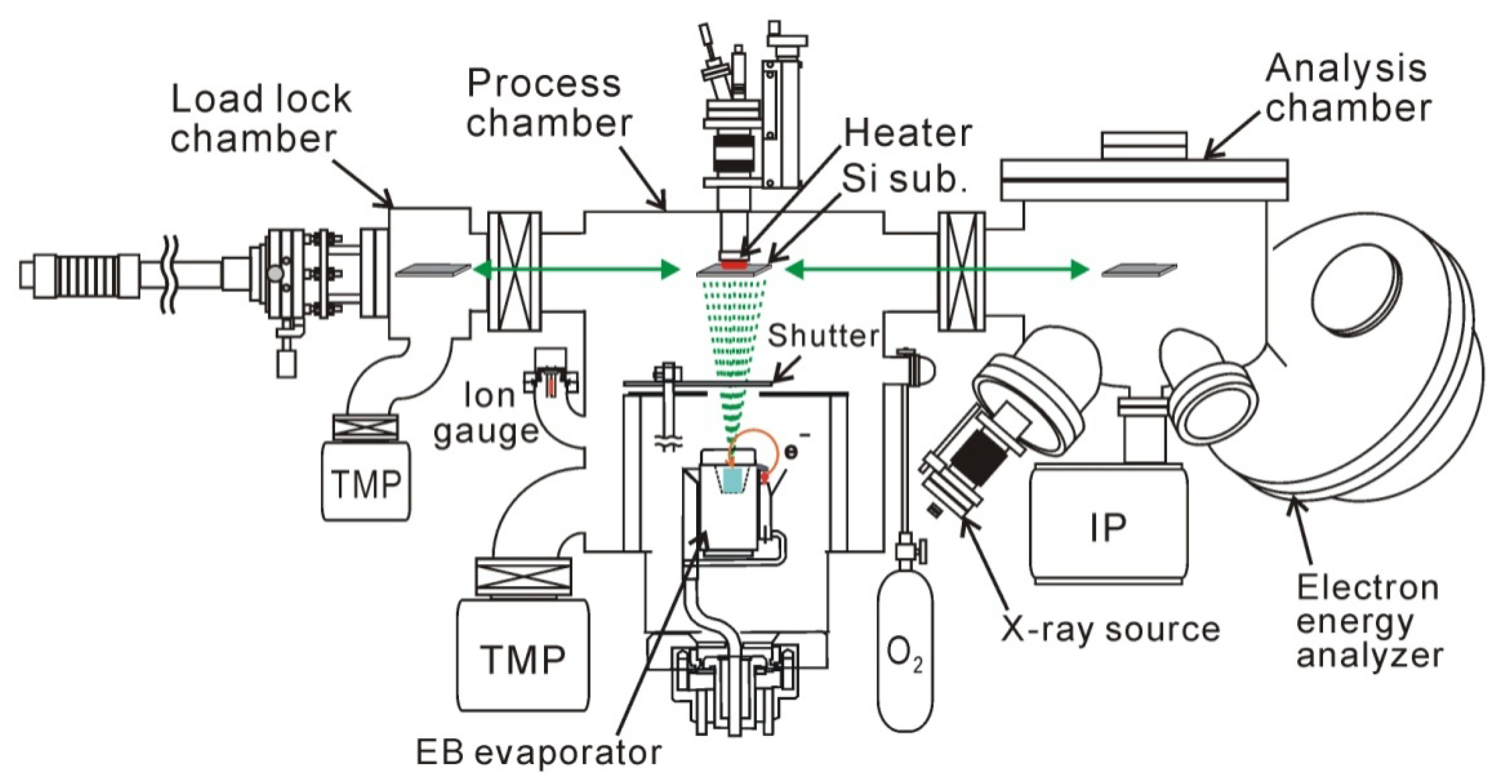
We should carefully choose process conditions by taking into account fundamental reactions in the HfO2/Si system. Interface layer growth and silicidation are major reactions taking place during HfO2 deposition and PDA. The former is particularly important in EOT scaling. There have been numerous reports on the growth of interface layers; the major chemical components have been ascribed to be SiO2, although small numbers of Hf atoms have sometimes been included (i.e., Hf silicate) [14,15,16,17,18]. The fact that Si oxide was formed implies that the Si surface was oxidized during HfO2 deposition and PDA. Thus, it is important to suppress the oxygen that is supplied to the Si surface from the process ambient, even though a certain amount of oxygen is required to produce Hf oxide. Therefore, we needed to carefully examine a wide range of O2 pressures to find optimum process conditions. UHV-EB evaporation is suitable for such experiments, because we can easily control the oxidant (O2) pressure in the high-vacuum range. A metallic Hf source was evaporated under an O2 pressure of 10−4–10−8 torr (Figure 1) in our experiment. This deposition setup had a load lock chamber and a surface analysis system that involved x-ray photoelectron spectroscopy.
Figure 1.
Experimental setup used for HfO2 deposition, post-deposition annealing (PDA), and surface analysis. XPS system was connected to UHV-EB evaporation chamber for in-vacuum analysis of surface chemistry.
Figure 1.
Experimental setup used for HfO2 deposition, post-deposition annealing (PDA), and surface analysis. XPS system was connected to UHV-EB evaporation chamber for in-vacuum analysis of surface chemistry.

Three Si-oxidation stages should be taken into account at least in the current processes: (1) Si oxidation before HfO2 deposition; (2) Si oxidation during HfO2 deposition; and (3) Si oxidation during PDA. Controlling the third stage is particularly serious, as the oxidation rate is much faster due to the HfO2 catalytic effect and the raised sample temperature (>400 °C) [16]. This issue will be discussed in the next section. This section focuses on the first and second stages. A hydrogen-terminated Si (100) surface formed by diluted hydrofluoric (HF) acid solution was used as the initial surface, because it is stable under atmospheric conditions [19]. However, this Si surface is not very stable in a vacuum chamber, e.g., a filament of the ion gauge dissociates residual molecules to break H-Si bonds on the Si surface. The sample in this work was slowly evacuated in the load-lock chamber, and it was then transferred to the deposition chamber without turning on the ion gauge in the load-lock chamber. The in-vacuum x-ray photoelectron measurements revealed that the surface coverage of oxygen on the Si substrate was less than 5%.
A certain amount of oxygen should intentionally be introduced into the chamber to produce metal oxide in the process of HfO2 deposition. We can easily predict that oxygen molecules will be dissociated by the filament of the ion gauge and of the EB evaporator as well as by the heated Hf source. The dissociated species immediately oxidizes the surface Si before and during HfO2 deposition. Thus, the ion gauge was carefully placed to prevent direct incidence of hot-filament-dissociated species onto the Si surface. The EB evaporator was separated from the sample with a water-cooled housing and shutter. The HfO2 was deposited at about 0.2 nm/min under an O2 pressure of 2 × 10⁻⁶ torr. The sample heater was turned off to suppress Si oxidation. Although radiation from the EB evaporator slightly raised the sample temperature, this was confirmed to be less than 100 °C by thermocouple measurement of the sample surface. The Si 2p photoelectron spectra revealed that the Si oxide was less than 0.15 nm thick after HfO2 deposition, suggesting the interface Si-O bonds were less than one monolayer [20]. The Hf 4f photoelectron spectra exhibited stoichiometric HfO2, even though the deposition was carried out under such low O2 pressure and low temperature conditions.
Although the XPS revealed stoichiometric HfO2, small numbers of defects were likely formed in the as-deposited HfO2. The MOS capacitors of the HfO2/Si structure actually showed unusual C-V curves and hysteresis. Therefore, PDA was required to eliminate the defects. Note that if the sample was exposed to air before PDA, fixed positive charges were created in HfO2 due to the reaction between defects with moisture [21,22]. This type of electric charge can be eliminated by using PDA, but high temperature annealing is required (>600 °C). Thus, in-situ PDA in the EB deposition chamber was performed in this experiment.
3. Kinetics of Interface Si Oxidation in PDA
As was described in the last section, interface Si-O bonds could be suppressed to less than one monolayer by employing UHV-EB deposition HfO2 method. Searching for optimum PDA conditions was more complicated, because of immediate Si oxidation due to the HfO2 catalytic effect and local silicidation. The Si oxide layer increased in thickness with increasing temperature and O2 pressure, while the annealing time was fixed (~several minutes) [16]. Under low O2 pressure conditions (<10−6 torr), on the other hand, local silicidation took place at temperatures higher than 800 °C [16]. Atomistic mass transfer on the HfO2 surface led to local thinning of the HfO2 layer, and this resulted in the formation of voids [23,24]. Hf silicide was formed in these voids due to the reaction of HfO2 with mobile Si atoms on the void surfaces (HfO2 + 4Si → HfSi2 + 2SiO↑) [25]. Since Hf silicide is metallic, MOS devices that underwent this silicidation did not work. The maximum PDA temperature that can suppress silicidation depends on the duration of PDA, as void formation is a time-development phenomenon. For typical durations of several minutes, we should chose a PDA temperature that is below 800 °C to suppress silicidation.
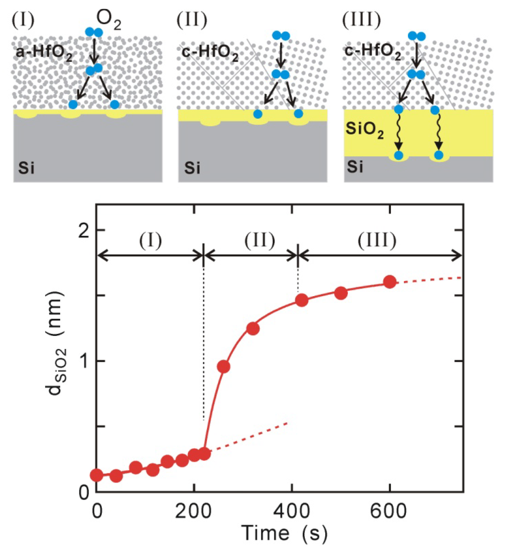
The thicknesses of Si oxide layers observed by XPS for the 1.5-nm-thick HfO2/Si structures are plotted in Figure 2, where PDA was performed at an O2 pressure of 2 × 10⁻⁶ torr at 400–500 °C. Si oxidation occurs in three stages: (I) slow oxidation in the monolayer range, (II) rapid oxidation up to thick SiO2 layers that exceed 1 nm, and (III) again slow oxidation showing saturated behavior. This indicates that PDA should be finished within stage (I) to maintain a direct-contact HfO2/Si interface. The activation energy for the first stage was estimated to be 0.3 eV, i.e., the dependence on temperature was very weak [20]. This characteristic acts as an advantage from the viewpoint of controlling interface Si oxidation. The PDA in this work was thus conducted under these conditions, i.e., an O2 pressure of 2 × 10⁻⁶ torr at 400–600 °C for several minutes.
Next, I will briefly explain why the mode of Si oxidation changes so dramatically during PDA. Although the oxidation rate in the first stage is smaller than those in the other stages, it is slightly higher than that on a clean Si(100)-2 × 1 surface. This means that atomic oxygen produced by defects in the as-deposited HfO2 layer contributes to Si oxidation even in the first stage. The crystallization of HfO2 in the second stage is responsible for the change in the mode of oxidation. The TEM observations actually revealed that a monoclinic HfO2 phase appeared in the second stage, although an amorphous HfO2 phase was maintained in the first stage [20]. This suggests that O2-dissociation sites, i.e., defects (e.g., oxygen vacancies), are largely created by crystallization. As oxygen diffusion in the third stage through the grown interface SiO2 layer limited the whole oxidation process, the oxidation rate was saturated. The activation energy in this stage has been reported to be 0.72 eV, which is smaller than the 1.24 eV reported for O2 diffusion through the SiO2 layer [26,27]. This means that atomic oxygen is a major oxidant species in Si oxidation in the HfO2/Si system.
Figure 2.
Si oxidation at 1.5-nm HfO2/Si interface during PDA in O2 pressure of 2 × 10⁻⁶ torr at 400–500 °C. Oxidation occurred in three steps of (I) slow oxidation in range of monolayer Si oxide; (II) rapid oxidation up to thick SiO2 layer exceeding 1 nm; and (III) slow oxidation demonstrating saturated behavior. Oxidation mechanisms expected for stages (I)–(III) have been depicted.
According to the above results, suppressing HfO2 crystallization is crucial to control interface Si oxide in the monolayer range. It has been reported that Al-, Si-, or N-incorporated HfO2 has an advantage in suppressing the growth of the interface layer. This is likely related to crystallization, i.e., the incorporation of such atoms is expected to increase the temperature of crystallization. Furthermore, the insertion of an oxygen-diffusion-barrier layer into the HfO2/Si system e.g., Al oxide or Si nitride, effectively suppresses Si oxidation [26,28]. However, as their dielectric constants are lower than that of HfO2, these multi-stack structures are not suitable for achieving an EOT of ~0.5 nm. Incorporating additional atoms or an oxygen-diffusion-barrier layer is probably required while the sample undergoes high-temperature PDA (>600 °C). A simple HfO2/Si structure can be applied for fabricating a direct-contact HfO2/Si structure in low-temperature PDA (≤600 °C).
4. MOS Electrical Characteristics
As previously described, UHV-EB HfO2 deposition and in-situ PDA enabled a direct-contact HfO2/Si structure with stoichiometric HfO2 to be prepared and interface Si-O bonds of about one monolayer to be attained. The electrical characteristics of MOS capacitors are reviewed in this section. It has been reported that the EOT values for direct-contact 2.2-nm-thick HfO2/n-Si(100) MOS capacitors have been estimated to be 0.45–0.48 nm from their high-frequency C-V curves [20]. The dependence of EOTs on HfO2 thickness has indicated that the dielectric constant of the HfO2 layer is about 20. This value is approximately consistent with that of bulk HfO2, supporting the formation of a stoichiometric HfO2 layer [4]. The dependence on thickness has also supported the argument that the interface layer is about zero for MOS capacitors fabricated on n-type Si substrates. However, the accumulation capacitances of MOS capacitors on p-type Si substrates were slightly smaller than those on n-type Si substrates, where additional layers with an EOT of ~0.26 nm virtually existed at HfO2/Si interfaces [29]. However, XPS observations did not reveal any differences in the interface Si oxide. This unexpected reduction in accumulation capacitance at the p-Si substrate could be explained based on the effect of the interface dipole, i.e., the hole distribution for the p-Si surface is slightly shifted far from the HfO2/Si interface due to the electrostatic potential of the interface dipole. We should note that this effect acts as a disadvantage in the operation of p-channel MOSFETs.
Interface state density (Dit) can roughly be inferred from the frequency dispersion in C-V curves. The C-V frequency dispersion of direct-contact HfO2/Si MOS capacitors has suggested that Dit near the mid-gap energy is on the order of 1011 cm−2eV−1 or less. A method of ac-conductance, which is more accurate, actually indicates a Dit of ~1011 cm−2eV−1 at around the mid-gap energy [30]. This is approximately equal to those of HfO2/SiO2/Si stack structures prepared with the same methods of UHV-EB and in-situ PDA. The MOSFET characteristics also support the small Dit, as will be explained in what follows. Thus, we can conclude that Si dangling bonds at the direct-contact HfO2/Si interface are effectively suppressed even though interface Si-O bonds are in the range of about one monolayer.
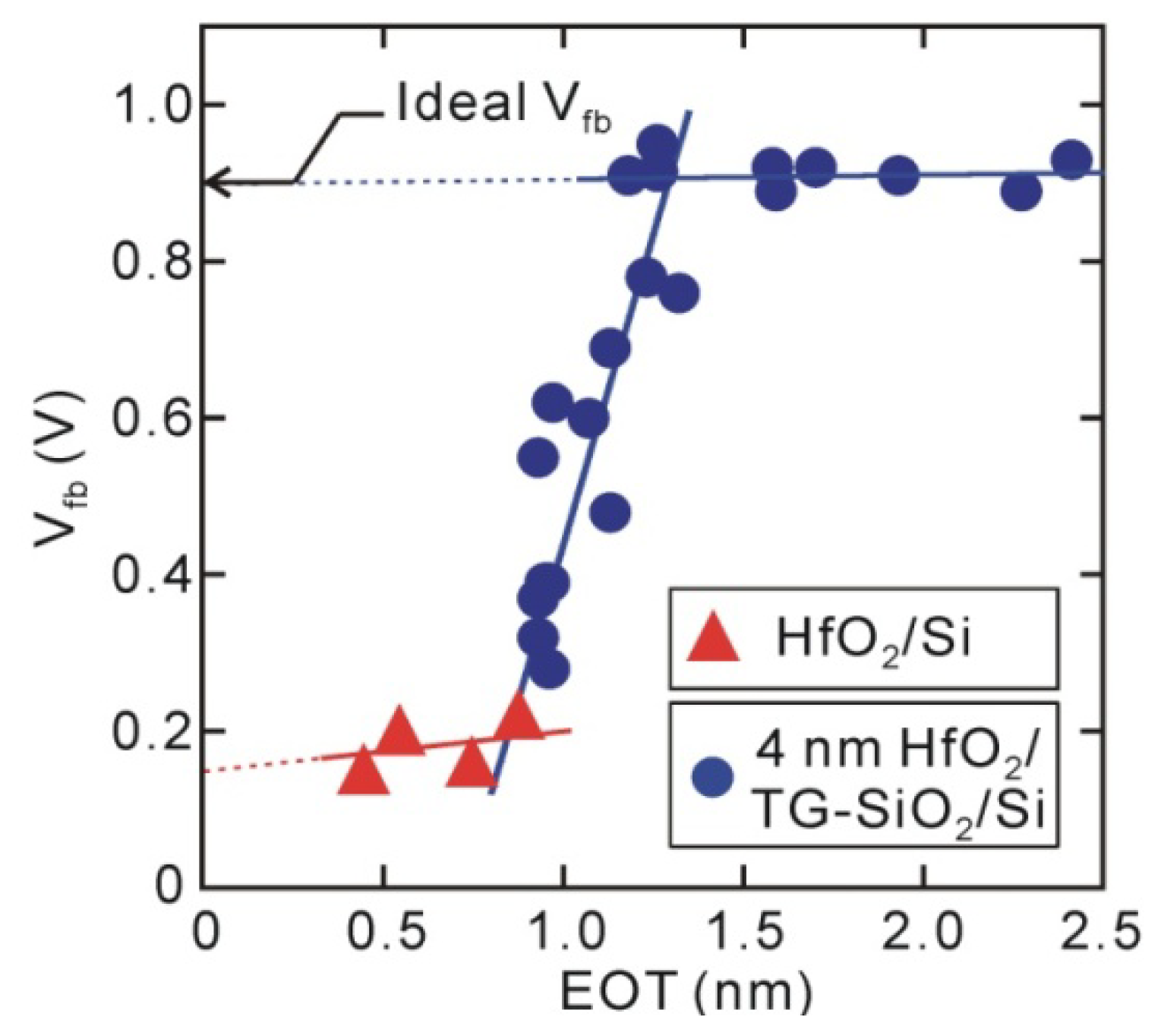
Next, let us discuss the distribution of fixed electric charges in the direct-contact HfO2/Si structures from the behavior of flat-band voltages (Vfb). The direct-contact samples demonstrated the obvious negative Vfb shifts shown in Figure 3, and their values did not depend on the HfO2 thickness. Unipolar-electric charges that exist at the oxide/Si interface usually show a Vfb shift that is dependent on oxide thickness, but dipole-like charges show Vfb shift that is independent of thickness [31]. Thus, it has been concluded that direct-contact HfO2/Si MOS capacitors have a strong interface dipole (>0.5 V, positively charged Si and negatively charged HfO2 sides) [32]. However, the HfO2/SiO2/Si stack structures with thick interface SiO2 layers have almost ideal Vfb. The Vfb behavior observed for the HfO2/thickness-graded (TG) SiO2/Si structure in Figure 3 reveals that negative Vfb shift in the direct-contact samples is almost completely mitigated by inserting an SiO2 layer that is about 0.5 nm thick, meaning that the interface dipole was eliminated by inserting an additional Si-O layer that was 3–4 monolayers. Thus, an interface dipole observed for the direct-contact HfO2/Si structure presumably exists at the HfO2/Si interface. Similar interface dipoles that are larger than 0.5 V have been observed from direct-contact HfO2/Ge structures that have interface Ge-O bonds of about one monolayer [33].
Figure 3.
Vfb for direct-contact HfO2/Si and 4 nm HfO2/TG-SiO2/Si MOS capacitors. Negative Vfb shift for direct-contact HfO2/Si MOS capacitor is mitigated by insertion of thin Si oxide layer (~0.5 nm).
Figure 3.
Vfb for direct-contact HfO2/Si and 4 nm HfO2/TG-SiO2/Si MOS capacitors. Negative Vfb shift for direct-contact HfO2/Si MOS capacitor is mitigated by insertion of thin Si oxide layer (~0.5 nm).

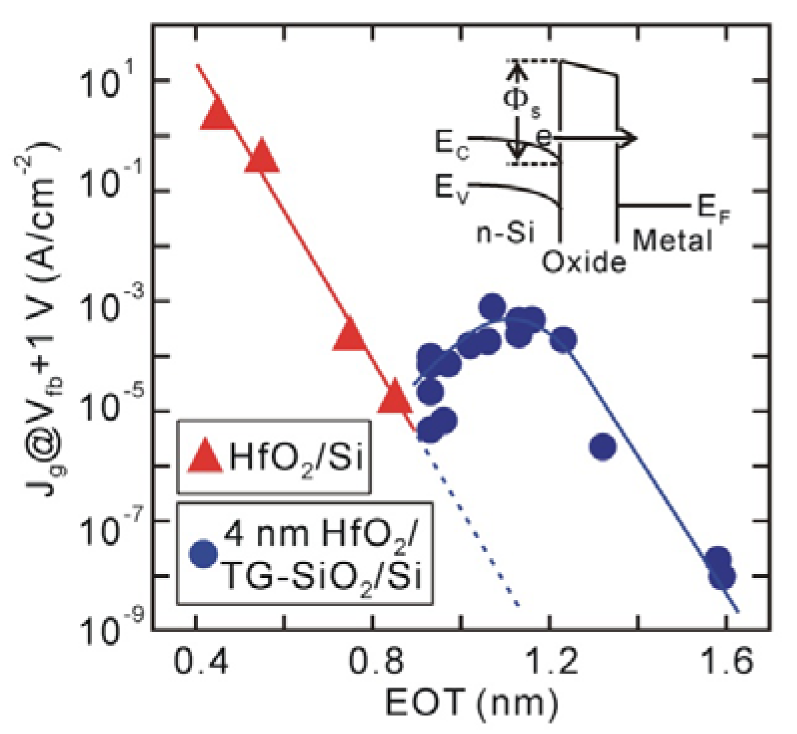
The leakage current (Jg) characteristics also support the existence of an interface dipole (Figure 4). Generally, Jg exponentially decreases with increasing dielectric layer thickness, while trap-assisted current is sufficiently suppressed, as those of the direct-contact HfO2/Si structures in Figure 4 show. This means that both conduction band offset (Φs) at the HfO2/Si interface and HfO2 thickness govern electron tunneling. Since the conduction band offset of the SiO2/Si interface (Φs ~3.15 eV) [34] is larger than that of the HfO2/Si interface (Φs ~1.1–1.5 eV) [35,36,37], the leakage current is expected to decrease by inserting an Si oxide layer, as indicated by the dotted line in Figure 4. However, the Jg of HfO2/TG-SiO2/Si MOS capacitors increases once and then decreases, probably meaning that the barrier height is reduced by the insertion of an interface Si oxide. In addition, the Φs values at the direct-contact HfO2/Si interfaces were estimated to be about 2.0 eV, which were obtained by fitting the measured Jg curves with a direct-tunneling model. This estimated barrier height is larger by at least 0.5 eV than those previously reported for HfO2/Si systems [35,36,37], suggesting that the conduction band offset at the direct-contact HfO2/Si interface is raised by the interface dipole [32].
Figure 4.
Jg at Vfb + 1 V for direct-contact HfO2/Si and 4 nm HfO2/TG-SiO2/Si MOS capacitors fabricated on n-type Si substrates. Jg for HfO2/TG-SiO2/Si MOS capacitors increases with increasing Si oxide layer because of reduced conduction band offset (Φs) at HfO2/Si interface.
Figure 4.
Jg at Vfb + 1 V for direct-contact HfO2/Si and 4 nm HfO2/TG-SiO2/Si MOS capacitors fabricated on n-type Si substrates. Jg for HfO2/TG-SiO2/Si MOS capacitors increases with increasing Si oxide layer because of reduced conduction band offset (Φs) at HfO2/Si interface.
5. Origin of Interface Dipole
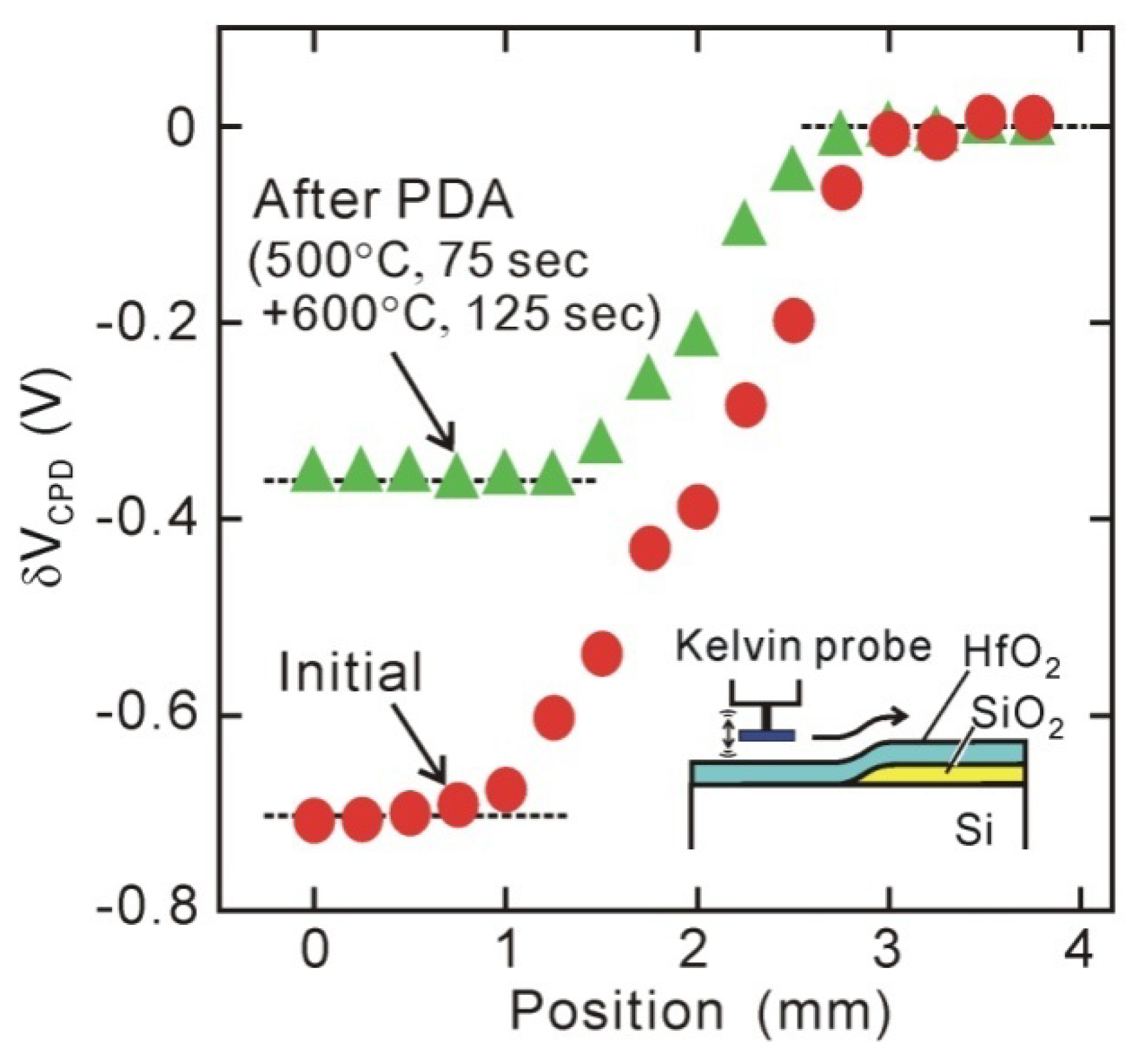
This section discusses the physical origin as to why a strong interface dipole was formed in direct-contact HfO2/Si MOS capacitors. First, we should examine extrinsic effects, e.g., the fabrication process for metal gates induces electric charges in gate stack structure [38,39]. As-prepared HfO2/Si samples should be evaluated with some surface analysis without gate metal layers being deposited to investigate such effects. X-ray photoelectron spectroscopy (XPS) is a potential method, which has often been used to identify the band lineups of oxide/semiconductor systems [40,41]. Our group employed hard x-ray photoemission spectroscopy as well as conventional XPS (Al kα x-ray source) to compare metal/HfO2/Si and HfO2/Si structures, but we could not find clear evidence that supported the existence of an interface dipole, because x-ray-induced electrical charges and screening effects around the HfO2/Si interface hampered band lineups from being accurately estimated [42]. Thus, Kelvin probe measurements, which are not accompanied by the creation of electrical charges in the oxide, were used to explore the origin of dipole formation.
The Kelvin probe measurement is a conventional surface analysis, which has widely been used to measure the work function of metal surfaces. A reference electrode was placed on the sample surface with a small air or vacuum gap (0.1–0.5 mm). The alternating current induced by vibrating the reference electrode was monitored to determine the contact potential difference (CPD) between the sample metal and reference electrode surfaces. The surface carrier response should be taken into account for the semiconductor surface, but an n-type semiconductor surface can be analyzed like a metal surface provided that the response of holes can be neglected. The band diagram for the oxide/Si surface is quite similar to that obtained from MOS measurements except for the vacuum gap [43,44]. Thus, we can infer the distribution of electric charges inside the oxide/Si structure from the behavior of VCPD. Figure 5 plots the normalized CPD voltage (δVCPD) observed from the sample surface that includes both direct-contact HfO2/Si and HfO2/SiO2/Si stack structures, which indicates that the surface potential of the direct-contact HfO2/Si area is smaller by about 0.7 V than that of the HfO2/SiO2/Si stack area [44,45]. This potential difference is approximately consistent with the negative Vfb shifts of MOS capacitors. This means that the interface dipole is formed before the metal gate is fabricated.
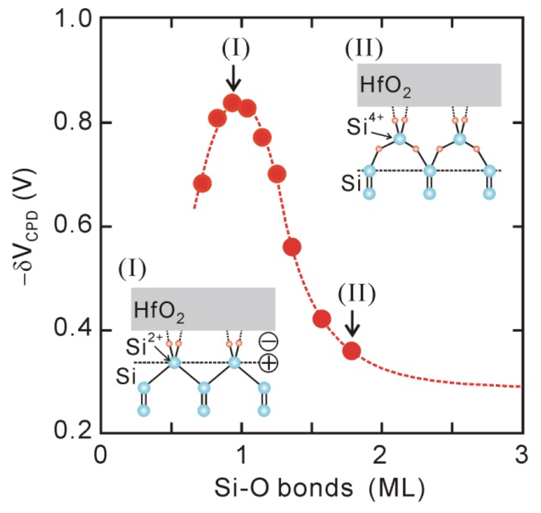
In-situ Kelvin probes and XPS have been used to assess the effect of interface chemical bonding on the interface dipole. Figure 6 plots the δVCPD values for direct-contact HfO2 (1.5 nm)/Si structures that underwent various PDA in the first oxidation stage in Figure 2, as a function of the thickness of the Si-O layer. The dipole strength becomes maximal at Si-O bonds of about one monolayer, and then decreases in the range of Si-O bonds of 1–2 monolayers. This behavior means that Si-O bonds of one monolayer are responsible for the interface dipole, and inserting oxygen atoms into the back bonds of these surface Si atoms results in the dipole being annihilated as shown in the insets in Figure 6. In addition, it has been reported that the interface dipole completely disappears while the interface Si-O bonds thermally decompose in UHV [45]. Similar annihilation of the dipole could be found for direct-contact HfO2/Ge structures [33]. Thus, we can conclude that the Si-O bonds of about one monolayer at the HfO2/Si interface mainly induce the interface dipole [44,45].
Figure 5.
In-situ Kelvin probe measurements for normalized contact potential difference (δVCPD). Large δVCPD difference between direct-contact HfO2/Si and HfO2/SiO2/Si stack structures indicates existence of interface dipole.
Figure 5.
In-situ Kelvin probe measurements for normalized contact potential difference (δVCPD). Large δVCPD difference between direct-contact HfO2/Si and HfO2/SiO2/Si stack structures indicates existence of interface dipole.

Figure 6.
δVCPD for direct-contact HfO2/Si structures after various PDA processes, as a function of Si-O thickness estimated by in-vacuum XPS.
Figure 6.
δVCPD for direct-contact HfO2/Si structures after various PDA processes, as a function of Si-O thickness estimated by in-vacuum XPS.
The formation of an interface dipole has been a long-standing controversy in the engineering of band lineups in metal/semiconductor, semiconductor/semiconductor, and oxide/semiconductor systems. Various mechanisms have been proposed, which can be roughly classified into two models. The first is charge transfer due to interface states, e.g., metal-induced-gap states (MIGS) and dielectric-constant-induced gap states (DCIGS) [46,47,48,49]. The second is based on the electric polarization of interface chemical bonds [50,51,52]. The C-V and ac-conductance measurements revealed that charge trapping at the direct-contact HfO2/Si interface is not serious as previously mentioned [30], so that the contribution of the first model is not as large in this case. Thus, the second model is preferable, as the Kelvin probe measurements demonstrated. However, it has widely been accepted that SiO2/Si structures, which are prepared by using appropriate thermal oxidation processes, do not have such strong dipoles, even though there are Si-O bonds at this interface. The author’s group thus compared electrostatic potential between atomistic models of SiO2/Si and direct-contact HfO2/Si interfaces [44]. As for the SiO2/Si interface, the potential on the SiO2 side is expected to be close to that on the Si side, as the potential drop by the interface Si-O bonds is compensated by the potential rise by the upper O-Si bonds. However, the potential rise by the O-Hf bonds in the direct-contact HfO2/Si interface was estimated to be smaller than that by the O-Si bonds in the SiO2/Si interface, as the dielectric constant for the O-Hf region was expected to be larger than that for the O-Si region. We, therefore, concluded that a dipole formation is a natural phenomenon for the atomically abrupt high-k/Si interface having one-monolayer Si-O bonds.
6. MOSFET Characteristics and Channel Mobility
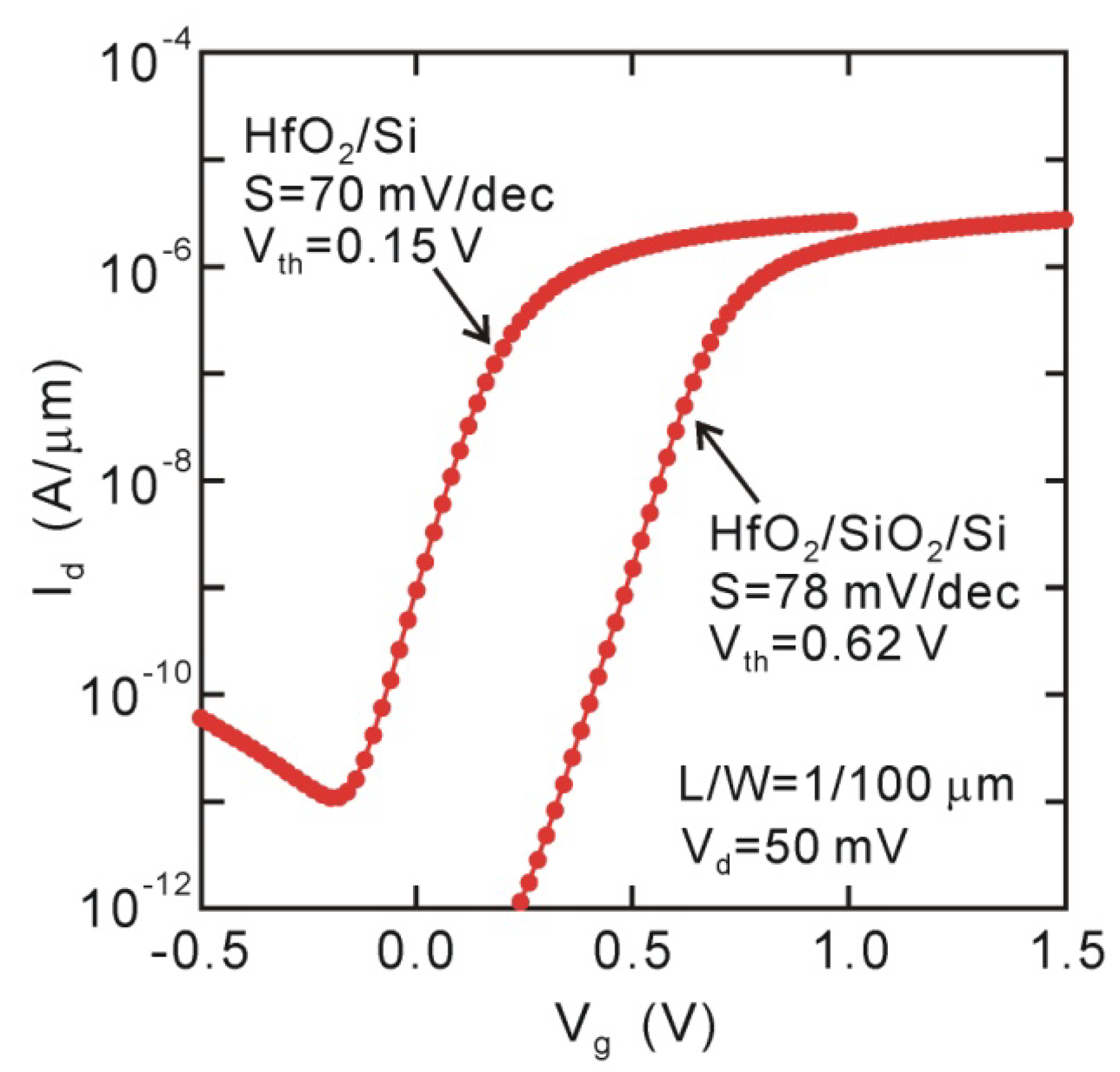
As previously described, direct-contact HfO2/Si structures have an advantage in EOT scaling in ranges thinner than 1 nm. The interface state density could be suppressed to ~1011 cm−2eV−1 at around the midgap, probably because of surface termination with Si-O bonds of about one monolayer. Thus, we could expect MOSFETs to work well except for the effect of the interface dipole. The Id-Vg curves for the direct-contact HfO2/Si MOSFET in Figure 7 actually indicate good behavioral characteristics. The Ion/Ioff ratio is larger than 105, even though a very thin HfO2 layer of 2.5 nm was used in the direct-contact HfO2/Si structure (EOT ~0.52 nm) [20]. The subthreshold slope (SS) was almost independent of the interface structures (SS ~70 mV/decay), which is approximately consistent with the Dit value estimated with the ac-conductance measurement of MOS capacitors. Obvious negative Vth shift can be identified in Figure 7, as predicted from the interface dipole observed for the MOS capacitors.
Figure 7.
Id-Vg curves of 2.5 nm HfO2/Si and HfO2/SiO2/Si MOSFETs. Large negative Vth shift takes place for direct-contact HfO2/Si device.
Figure 7.
Id-Vg curves of 2.5 nm HfO2/Si and HfO2/SiO2/Si MOSFETs. Large negative Vth shift takes place for direct-contact HfO2/Si device.

The impact of interface dipoles on channel mobility has been pointed out in several papers, e.g., high-k/Si and high-k/III-V-channel MOSFETs [53,54,55]. Actually, electron mobility of direct-contact HfO2/Si MOSFET is smaller than that of HfO2/SiO2/Si stack MOSFET, as shown in Figure 8(a). Thus, we have examined what effect such an interface dipole has on the channel mobility of direct-contact HfO2/Si MOSFETs. The channel mobility of high-k-gated MOSFETs generally gradually decreases with thinning interface Si oxide layers (IL) due to the so-called remote scattering, i.e., high-k phonon scattering and Coulomb scattering due to oxide charges in the high-k layer [56,57,58,59]. We should take such effects into account to identify the true impact of dipoles. Actually, additional electron mobility (µadd) decreases exponentially throughout the whole tIL range including direct-contact HfO2/Si interfaces, as seen in Figure 8(b). This tendency suggests that remote scattering is the dominant mechanism [56,57,58,59]. The variable temperature measurements suggested that remote scattering could mainly be ascribed to Coulomb effects due to oxide charges in the HfO2 layer [60]. The incorporation of nitrogen into HfO2 effectively reduced the oxide charges, as the HfON/HfO2/Si stack device had larger channel mobility than standard HfO2/Si device [Figure 8(a,b)].
Figure 8.
Electron mobility characteristics of HfO2/Si and HfON/HfO2/Si MOSFETs. (a) Effective mobility characteristics; and (b) additional electron mobility (μadd@Ns = 1.82 × 1012 cm−2) for 3.5-nm HfO2/TG-SiO2/Si and 3-nm HfON/0.5-nm HfO2/Si MOSFETs.
Figure 8.
Electron mobility characteristics of HfO2/Si and HfON/HfO2/Si MOSFETs. (a) Effective mobility characteristics; and (b) additional electron mobility (μadd@Ns = 1.82 × 1012 cm−2) for 3.5-nm HfO2/TG-SiO2/Si and 3-nm HfON/0.5-nm HfO2/Si MOSFETs.
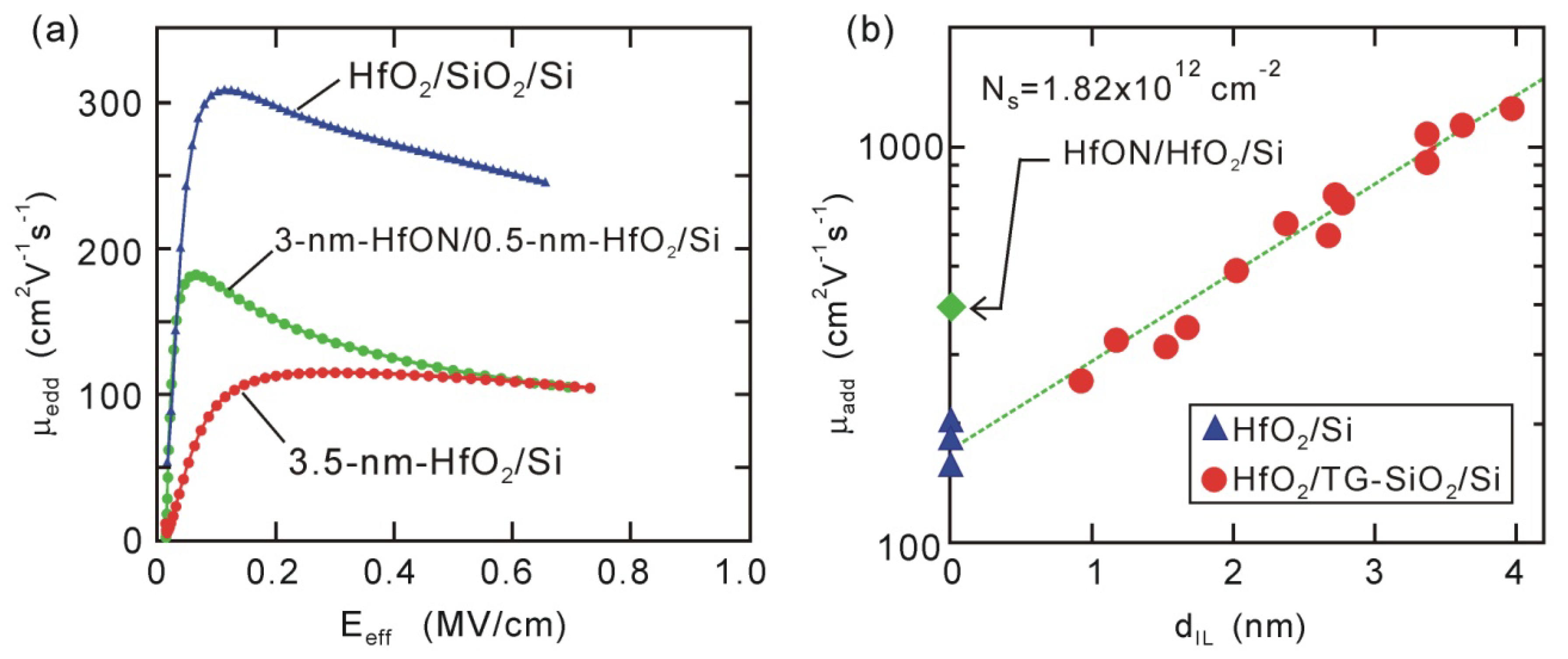
If the dipole had some impact, a dramatic change should have been observed in the dependence of µadd on tIL, as the negative Vfb and Vth shifts were mitigated by inserting a ~0.5 nm thick Si oxide layer. It is obvious that the data observed in Figure 8(b) do not demonstrate such a dramatic change. In addition, the µadd of direct-contact HfO2/Si devices depended on the HfO2 thickness [60], although the dipole strength was nearly independent of the HfO2 thickness [32]. Thus, we can conclude that dipole scattering is not the dominant mechanism responsible for degradation in direct-contact HfO2/Si devices. We can expect that well-ordered dipoles, which do not produce large electrostatic potential fluctuations, do not act as strong scattering centers, e.g., interface chemical bonds at lattice-matched heterojunctions do not induce serious degradation in mobility [61]. The present results suggest that uniformly arrayed dipoles are formed at direct-contact HfO2/Si interfaces. This speculation is consistent with the above dipole model based on the electrostatic potential of interface Si-O and O-Hf bonds [44,45].
7. Conclusions
UHV-EB HfO2 deposition and in-situ PDA enabled us to prepare the so-called direct-contact HfO2/Si structure. The electrical characteristics of direct-contact HfO2/Si MOS capacitors demonstrated low interface state density but a strong interface dipole. The in-situ Kelvin probe measurements of HfO2/Si structures provided clear evidence for the formation of dipoles at direct-contact HfO2/Si interfaces. It is proposed that Si-O bonds of about one monolayer at the HfO2/Si interface naturally lead to large differences in the electrostatic potential due to the large dielectric constant of HfO2. It was also found that dipole scattering in direct-contact HfO2/Si MOSFETs is not of major concern in terms of the mobility criterion.
Acknowledgments
The author would like to thank T. Yasuda, M. Ichikawa, M. Kundu, and Y. Abe for their helpful discussion and comments. This work was partly supported by a Grant-in-Aid for Scientific Research (B) (No. 19360149) from the Japan Society for the Promotion of Science (JSPS). A Part of this work was performed at the Nano-Processing Facility (NPF) of AIST.
References
- Mistry, K.; Allen, C.; Auth, C.; Beattie, B.; Bergstrom, D.; Bost, M.; Brazier, M.; Buehler, M.; Cappellani, A.; Chau, R.; et al. A 45 nm logic technology with high-k + Metal gate transistors, strained silicon, 9 Cu interconnect layers, 193nm dry patterning, and 100% Pb-free packaging. In Proceeding of the IEEE International Electron Devices Meeting, Washington, DC, USA, 10–12 December 2007; pp. 247–245.
- Jan, C.-H.; Agostinelli, M.; Buehler, M.; Chen, Z.-P.; Choi, S.-J.; Curello, G.; Deshpande, H.; Gannavaram, S.; Hafez, W.; Jalan, U.; et al. A 32 nm SoC platform technology with 2nd generation high-k/metal gate transistors optimized for ultra low power, high performance, and high density product applications. In Proceeding of the IEEE International Electron Devices Meeting, Baltimore, MD, USA; 2009; pp. 1–4. [Google Scholar]
- Green, M.L.; Gusev, E.P.; Degraeve, R.; Garfunkel, E.L. Ultrathin (<4 nm) SiO2 and Si-O-N gate dielectric layers for silicon microelectronics: Understanding the processing, structure, and physical and electrical limits. J. Appl. Phys. 2001, 90, 2057–2122. [Google Scholar]
- Wilk, G.D.; Wallace, R.M.; Anthony, J.M. High-k gate dielectrics: Current status and materials properties considerations. J. Appl. Phys. 2001, 89, 5243–5276. [Google Scholar] [CrossRef]
- Qi, W.J.; Nieh, R; Lee, B.H.; Kang, L.; Jeon, Y; Onishi, K.; Ngai, T.; Banerjee, S.; Lee, J.C. MOSCAP and MOSFET characteristics using ZrO2 gate dielectric deposited directly on Si. In Proceeding of the IEEE International Electron Devices Meeting, Washington, DC, USA; 1999; pp. 145–148. [Google Scholar]
- Chin, A.; Wu, Y.H.; Chen, S.B.; Liao, C.C.; Chen, W.J. High quality La2O3 and Al2O3 gate dielectrics with equivalent oxide thickness 5–10 Å. In Proceeding of the VLSI Technology, Digest of Technical Papers, Honolulu, HI, USA; 2000; pp. 16–17. [Google Scholar]
- Ragnarsson, L.-A.; Guha, S.; Copel, M.; Cartier, E.; Bojarczuk, N. A.; Karasinski, J. Molecular-beam-deposited yttrium-oxide dielectrics in aluminum-gated metal-oxide-semiconductor field-effect transistors: Effective electron mobility. Appl. Phys. Lett. 2001, 78, 4169–4171. [Google Scholar] [CrossRef]
- Wu, Y.H.; Yang, M.Y.; Chin, A.; Chen, W.J.; Kwei, C.M. Electrical characteristics of high quality La2O3 gate dielectric with equivalent oxide thickness of 5 Å. Electron. Device Lett. 2000, 21, 341–343. [Google Scholar] [CrossRef]
- Peacock, P.W.; Xiong, K.; Tse, K.; Robertson, J. Bonding and interface states of Si: HfO2 and Si:ZrO2 interfaces. Phys. Rev. B 2006, 73, 075328. [Google Scholar] [CrossRef]
- Hobbs, C.; Fonseca, L.; Dhandapani, V.; Samavedam, S.; Taylor, B.; Grant, J.; Dip, L.; Triyoso, D.; Hegde, R.; Gilmer, D.; et al. Fermi level pinning at the poly Si/metal oxide interface. VLSI Tech. Dig. 2004, 51, 9–10. [Google Scholar]
- Akiyama, K.; Wang, W.; Mizubayashi, W.; Ikeda, M.; Ota, H.; Nabatame, T.; Toriumi, A. VFB roll-off in HfO2 gate stack after high temperature annealing process—A crucial role of out-diffused oxygen from HfO2 to Si. In Proceeding of the VLSI Technology, Tokyo, Japan; 2007; pp. 72–73. [Google Scholar]
- Ohmori, K.; Ahmet, P.; Shiraishi, K.; Yamabe, K.; Watanabe, H.; Akasaka, Y.; Umezawa, N.; Nakajima, K.; Yoshitake, M.; Nakayama, T.; et al. Controllability of flatband voltage in high-k gate stack structures—Remarkable advantages of La2O3/HfO2. In Proceeding of the Solid-State and Integrated Circuit Technology, 8th International Conference, Shanghai, China; 2006; pp. 376–379. [Google Scholar]
- The International Technology Roadmap for Semiconductor; Semiconductor Industry Association: San Jose, CA, USA, 2003. Available online: http://www.itrs.net (accessed on 6 March 2012).
- He, G.; Fang, Q.; Liu, M.; Zhu, L.Q.; Zhang, L.D. The structural and interfacial properties of HfO2/Si by the plasma oxidation of sputtered metallic Hf thin films. J. Cryst. Growth 2004, 268, 155–162. [Google Scholar] [CrossRef]
- Lee, M.; Lu, Z.-H.; Ng, W.-T.; Landheer, D.; Wu, X.; Moisa, S. Interfacial growth in HfOxNy gate dielectrics deposited using [(C2H5)2N]4Hf with O2 and NO. Appl. Phys. Lett. 2003, 83, 2638–2640. [Google Scholar] [CrossRef] [Green Version]
- Miyata, N.; Ichikawa, M.; Nabatame, T.; Horikawa, T.; Toriumi, A. Thermal stability of a thin HfO2/ultrathin SiO2/Si structure: Interfacial Si oxidation and silicidation. Jpn. J. Appl. Phys. 2003, 42, 138–140. [Google Scholar] [CrossRef]
- Kirsch, P.D.; Kang, C.S.; Lozano, J.; Lee, J.C.; Ekerdt, J.G. Electrical and spectroscopic comparison of HfO2/Si interfaces on nitrided and un-nitrided Si(100). J. Appl. Phys. 2002, 91, 4353–4364. [Google Scholar] [CrossRef]
- Cho, M.-H.; Roh, Y.S.; Whang, C.N.; Jeong, K.; Nahm, S.W.; Ko, D.-H.; Lee, J.H.; Lee, N.I.; Fujihara, K. Thermal stability and structural characteristics of HfO2 films on Si (100) grown by atomic-layer deposition. Appl. Phys. Lett. 2002, 81, 472–475. [Google Scholar] [CrossRef]
- Chabal, Y.J. Infrared spectroscopy of hydrogen on silicon surfaces. Physica. B Condens. Matter 1991, 170, 447–456. [Google Scholar] [CrossRef]
- Miyata, N. Two-step behavior of initial oxidation at HfO2/Si interface. Appl. Phys. Lett. 2006, 89, 102903:1–102903:3. [Google Scholar] [CrossRef]
- Miyata, N.; Ota, H.; Ichikawa, M. Correlation between scanning-tunneling-probe-induced spots and fixed positive charges in thin HfO2 films. Appl. Phys. Lett. 2005, 86, 112906:1–112906:3. [Google Scholar] [CrossRef]
- Miyata, N. Photoassisted scanning tunneling spectroscopy study on the local spot strucutres in thin HfO2 film on Si. Appl. Phys. Express 2008, 1, 051602:1–051602:3. [Google Scholar]
- Miyata, N.; Nabatame, T.; Horikawa, T.; Ichikawa, M.; Toriumi, A. Void nucleation in thin HfO2 layer on Si. Appl. Phys. Lett. 2003, 82, 3880–3883. [Google Scholar] [CrossRef]
- Miyata, N.; Yasuda, T.; Abe, Y. Structural degradation of thin HfO2 film on Ge during the post deposition annealing. J. Appl. Phys. 2010, 107, 103536–103541. [Google Scholar] [CrossRef]
- Miyata, N.; Morita, Y.; Horikawa, T.; Nabatame, T.; Ichikawa, M.; Toriumi, A. Two-dimensional void growth during thermal annealing of thin HfO2 film on Si. Phys. Rev. 2005, B71, 233302:1–233302:4. [Google Scholar]
- Kundu, M.; Miyata, N.; Nabatame, T.; Horikawa, T.; Ichikawa, M.; Toriumi, A. Effect of Al2O3 capping layer on suppression of interfacial SiO2 growth in HfO2/ultrathin SiO2/Si(001) structure. Appl. Phys. Lett. 2003, 82, 3442–3445. [Google Scholar] [CrossRef]
- Massoud, H.Z.; Plummer, J.D.; Irene, E.A. Thermal Oxidation of silicon in dry oxygen growth-rate enhancement in the thin regime. J. Electrochem. Soc. 1985, 132, 2685–2693. [Google Scholar] [CrossRef]
- Kundu, M.; Miyata, N.; Morita, Y.; Horikawa, T.; Nabatame, T.; Ichikawa, M.; Toriumi, A. Decomposition of SiN interlayer during thermal annealing of HfAlOx/SiN/Si(001) structure. Appl. Phys. Lett. 2004, 84, 5326–5328. [Google Scholar] [CrossRef]
- Abe, Y.; Miyata, N.; Nohira, H.; Yasuda, T. Reduction of accumulation capacitance in direct-contact HfO2/p-Type Si metal-oxide-semiconductor capacitors. Jpn. J. Appl. Phys. 2010, 49, 060202:1–060202:3. [Google Scholar]
- Miyata, N.; Abe, Y.; Yasuda, T. Conductance spectroscopy study on interface electronic states of HfO2/Si structures: Comparison with interface dipole. Appl. Phys. Express 2009, 2, 035502. [Google Scholar] [CrossRef]
- Hickmott, T.W. Dipole layers at the metal—SiO2 interface. J. Appl. Phys. 1980, 51, 4269–4281. [Google Scholar] [CrossRef]
- Abe, Y.; Miyata, N.; Shiraki, Y.; Yasuda, T. Dipole formation at direct-contact HfO2/Si interface. Appl. Phys. Lett. 2007, 90, 172906:1–172906:3. [Google Scholar]
- Abe, Y.; Miyata, N.; Yasuda, T. Comparison between the direct-contact HfO2/Ge and HfO2/SiO2/Ge structure: Physical and electrical properties. ECS Trans. 2008, 375, 375–385. [Google Scholar]
- Sze, M. Physics of Semiconductor Devices, 2nd Ed. ed; Wiley: New York, NY, USA, 1981. [Google Scholar]
- Robertson, J. Band offsets of wide-band-gap oxides and implications for future electronic devices. J. Vac. Sci. Technol. 2000, B18, 1785–1791. [Google Scholar] [CrossRef]
- Zhu, W.J.; Tso-Ping Ma; Tamagawa, T.; Kim, J.; Di, Y. Current transport in metal/hafnium oxide/silicon structure. IEEE Electron. Device Lett. 2002, 23, 97–99. [Google Scholar] [CrossRef]
- Tanimura, T.; Toyoda, S.; Kumigashira, H.; Oshima, M.; Ikeda, K.; Liu, G.L.; Liu, Z.; Usuda, K. Analysis of x-ray irradiation effect in high-k gate dielectrics by time-dependent photoemission spectroscopy using synchrotron radiation. Surf. Interface Anal. 2008, 40, 1606–1609. [Google Scholar] [CrossRef]
- Kadoshima, M.; Ogawa, A.; Ota, H.; Iwamoto, K.; Takahashi, M.; Mise, N.; Migita, S.; Ikeda, M.; Satake, H.; Nabatame, T.; Toriumi, A. Symmetrical threshold voltage in complementary metal-oxide-semiconductor field-effect transistors with HfAlOx(N) achieved by adjusting Hf/Al compositional ratio. J. Appl. Phys. 2006, 99, 054506:1–054506:6. [Google Scholar] [CrossRef]
- Akasaka, Y.; Nakamura, G.; Shiraishi, K.; Umezawa, N.; Yamabe, K.; Ogawa, O.; Lee, M.; Amiaka, T.; Kasuya, T.; Watanabe, H.; et al. Modified oxygen vacancy induced fermi level pinning model extendable to P-metal pinning. Jpn. J. Appl. Phys. 2006, 45, L1289–L1291. [Google Scholar] [CrossRef]
- Miyazaki, S. Photoemission study of energy-band alignments and gap-state density distributions for high-k gate dielectrics. J. Vac. Sci. Technol. 2001, B19, 2212–2216. [Google Scholar] [CrossRef]
- Oshima, M.; Toyoda, S.; Okumura, T.; Okabayashi, J.; Kumigashira, H.; Ono, K.; Niwa, M.; Usuda, K.; Hirashita, N. Chemistry and band offsets of HfO2 thin films for gate insulators. Appl. Phys. Lett. 2003, 83, 2172–2175. [Google Scholar] [CrossRef]
- Abe, Y.; Miyata, N.; Ikenaga, E.; Suzuki, H.; Kitamura, K.; Igarashi, S.; Nohira, H. Effect of oxide charge trapping on x-ray photoelectron spectroscopy of HfO2/SiO2/Si structures. Jpn. J. Appl. Phys. 2009, 48, 7999–8004. [Google Scholar]
- Schroder, D.K. Surface voltage and surface photovoltage: History, theory and applications. Meas. Sci. Technol. 2001, 12, R16–R31. [Google Scholar] [CrossRef]
- Miyata, N.; Yasuda, T.; Abe, Y. Kelvin probe study on formation of electric dipole at direct-contact HfO2/Si interfaces. J. Appl. Phys. 2011, 110, 074115:1–074115:8. [Google Scholar] [CrossRef]
- Miyata, N.; Yasuda, T.; Abe, Y. Kelvin probe study of dipole formation and annihilation at the HfO2/Si interface. Appl. Phys. Express 2010, 3, 054101:1–054101:3. [Google Scholar]
- Bardeen, J. Surface states and rectification at a metal semi-conductor contact. Phys. Rev. 1947, 71, 717–727. [Google Scholar] [CrossRef]
- Tersoff, J. Theory of semiconductor heterojunctions: The role of quantum dipoles. Phys. Rev. 1984, B 30, 4874–4877. [Google Scholar] [CrossRef]
- Robertson, J. Band structures and band offsets of high K dielectrics on Si. Appl. Surf. Sci. 2002, 170, 2–7. [Google Scholar] [CrossRef]
- Mönch, W. On the electric-dipole contribution to the valence-band offsets in semiconductor-oxide heterostructures. Appl. Phys. Lett. 2007, 91, 042117:1–042117:3. [Google Scholar] [CrossRef]
- Lambrecht, W.R.L; Segall, B. Self-consistent dipole theory of heterojunction band offsets. Phys. Rev. 1990, B41, 2831–2813. [Google Scholar]
- Tung, R.T. Formation of an electric dipole at metal-semiconductor interfaces. Phys. Rev. 2001, B64, 205310:1–205310:15. [Google Scholar]
- McKee, R.A.; Walker, F.J.; Nardelli, M.B.; Shelton, W.A.; Stocks, G.M. The interface phase and the schottky barrier for a crystalline dielectric on silicon. Science 2003, 300, 1726–1730. [Google Scholar] [CrossRef] [PubMed]
- Nara, Y. Dielectric Films for Advanced Microelectronics; Baklanov, M., Green, M., Maex, K., Eds.; Wiley: New York, NY, USA, 2007; p. 437. [Google Scholar]
- Ota, H.; Hirano, A.; Watanabe, Y.; Yasuda, N.; Iwamoto, K.; Akiyama, K.; Okada, K.; Migita, S.; Nabatame, T.; Toriumi, A. Intrinsic origin of electron mobility reduction in high-k mosfets—From remote phonon to bottom interface dipole scattering. In Proceeding of the IEEE International Electron Devices Meeting, Washington, DC, USA, 10–12 December 2007; pp. 65–68.
- Urabe, Y.; Miyata, N.; Ishii, H.; Itatani, T.; Maeda, T.; Yasuda, T.; Yamada, H.; Fukuhara, N.; Hata, M.; Yokoyama, M.; et al. Correlation between channel mobility improvements and negative Vth shifts in III–V MISFETs: Dipole fluctuation as new scattering mechanism. In Proceeding of the IEEE International Electron Devices Meeting, San Francisco, CA, USA, 6–8 December 2010; pp. 142–145.
- Fischetti, M.V.; Neumayer, D.A; Carter, E.A. Effective electron mobility in Si inversion layers in metal-oxide-semiconductor systems with a high-k insulator: The role of remote phonon scattering. J. Appl. Phys. 2001, 90, 4587–4609. [Google Scholar] [CrossRef]
- Yasuda, N.; Hisamatsu, H.; Ota, H.; Mizubayashi, W.; Toriumi, A. Weak temperature dependence of non-coulomb scattering component of HfAlOx-limited inversion layer mobility in n+-polysilicon/HfAlOx/SiO2 N-channel metal-oxide-semiconductor field-effect transistors. Jpn. J. Appl. Phys. 2005, 44, 7750–7755. [Google Scholar] [CrossRef]
- Weber, O.; Cassé, M.; Thevenod, L.; Ducroquet, F.; Ernst, T.; Deleonibus, S. On the mobility in high-k/metal gate MOSFETs: Evaluation of the high-k phonon scattering impact. Solid-State Electron. 2006, 50, 626–631. [Google Scholar] [CrossRef]
- Ando, T.; Copel, M.; Bruley, J.; Frank, M.; Martin, M.; Watanabe, H.; Narayanan, V. Physical Origins of mobility degradation in extremely scaled SiO2/HfO2 gate stacks with La and Al induced dipoles. Appl. Phys. Lett. 2010, 96, 132904:1–132904:3. [Google Scholar]
- Miyata, N.; Ishii, H.; Itatani, T.; Yasuda, T. Electron mobility degradation and interface dipole formation in direct-contact HfO2/Si metal-oxide-semiconductor field-effect transistors. Appl. Phys. Express 2011, 4, 101101:1–101101:3. [Google Scholar] [CrossRef]
- Zhao, W.; Jena, D. Dipole scattering in highly polar semiconductor alloys. J. Appl. Phys. 2004, 96, 2095–2101. [Google Scholar] [CrossRef]
© 2012 by the authors; licensee MDPI, Basel, Switzerland. This article is an open access article distributed under the terms and conditions of the Creative Commons Attribution license (http://creativecommons.org/licenses/by/3.0/).
Share and Cite
MDPI and ACS Style
Miyata, N. Study of Direct-Contact HfO2/Si Interfaces. Materials 2012, 5, 512-527. https://doi.org/10.3390/ma5030512
AMA Style
Miyata N. Study of Direct-Contact HfO2/Si Interfaces. Materials. 2012; 5(3):512-527. https://doi.org/10.3390/ma5030512
Chicago/Turabian StyleMiyata, Noriyuki. 2012. "Study of Direct-Contact HfO2/Si Interfaces" Materials 5, no. 3: 512-527. https://doi.org/10.3390/ma5030512