Emerging Applications for High K Materials in VLSI Technology

Abstract
: The current status of High K dielectrics in Very Large Scale Integrated circuit (VLSI) manufacturing for leading edge Dynamic Random Access Memory (DRAM) and Complementary Metal Oxide Semiconductor (CMOS) applications is summarized along with the deposition methods and general equipment types employed. Emerging applications for High K dielectrics in future CMOS are described as well for implementations in 10 nm and beyond nodes. Additional emerging applications for High K dielectrics include Resistive RAM memories, Metal-Insulator-Metal (MIM) diodes, Ferroelectric logic and memory devices, and as mask layers for patterning. Atomic Layer Deposition (ALD) is a common and proven deposition method for all of the applications discussed for use in future VLSI manufacturing.
1. Introduction
Over the past half century the economics of the semiconductor industry have been driven by the principle of Moore’s law, which is really the observation that as semiconductor manufacturing technology continually improves the minimum manufacturing cost per device is continually decreasing and is realized by doubling the number of devices per square unit area roughly every two years [1]. Thus, semiconductor device makers have continued to shrink or “scale” the footprint of their devices on the wafer at a relatively constant pace over the decades. The resulting increases in readily available computing power have been a boon to mankind and underpin most of the technological and scientific progress made in the past 50 years. The terminology of device nodes has arisen as a common way to reference each new two year cycle. The device node at one time equated to the half-pitch or spacing between the tightest metal lines in Dynamic Random Access Memory (DRAM) chips, then migrated to become the minimum feature size in a given chip (typically Flash memory), and now the device node is effectively a marketing term that continues to decrease linearly even if no feature on the chip can be found to match it. Nevertheless, the very real trend of doubling the number of devices per unit area biannually, first laid out by Gordon Moore in 1965, has continued steadily through nodes named in microns on to nanometer-scale nodes and very soon to nodes that one might suppose will be termed in angstroms [2].
In order to continue device scaling to the 45 nm and below nodes, semiconductor device makers have implemented High K and Metal Gate (HKMG) stacks within the Metal Oxide Semiconductor Field Effect Transistors (MOSFETs) used in digital Complementary Metal Oxide Semiconductor (CMOS) technology, which forms the basis for logic circuits within microprocessors and systems on a chip used in computers, tablets, cell phones, etc. [2,3]. Likewise, memory technologies, such as DRAM, have also migrated to High K dielectrics [4]. For the purpose of this review High K dielectrics refer to a class of simple binary and ternary metal oxide insulators with a relative dielectric constant greater than about 9 and comprising transition metals from groups 3–5, the lanthanides and Al. The relative dielectric constant, K, is defined according to Equation (1), where εd is the permittivity of the dielectric and ε0 is the permittivity of free space. Representative examples of High K dielectrics include Al2O3, HfO2, ZrO2, HfZrO4, TiO2, Sc2O3 Y2O3, La2O3, Lu2O3, Nb2O5, Ta2O5 and simple mixtures thereof. By replacing dielectrics such as SiO2 (K = 3.9) and SiON (K = 4–6) with High K dielectrics, CMOS and DRAM manufacturers were able to continue scaling the Equivalent Oxide Thickness (EOT) of their devices while simultaneously using a physically thicker dielectric resulting in a leakage current reduction versus the SiO2 and SiON based devices at the same EOT [2,4].
The use of High K dielectrics in manufacturing has paved the way for their use in applications beyond traditional logic and memory devices. As logic devices continue to evolve device makers are moving towards non-classical CMOS devices incorporating high mobility channel materials or new device architectures, which will also rely on potentially new High K dielectric stacks. Memory makers are similarly contemplating new memory devices and structures, such as Resistive Random Access Memory (ReRAM) and 3-dimensional stacked memories. In many cases the emerging applications of High K dielectrics rely on properties other than their dielectric constant. For example current conduction through the High K dielectric is used in ReRAM and controlled in many cases by ion migration within the dielectric to form conducting filaments. Because of its low deposition temperature and etch resistance, aluminum oxide may find use as a hard mask or as a sidewall spacer within double patterning schemes.
This review summarizes some of the emerging applications for High K dielectrics which may be implemented in future semiconductor manufacturing. The current status of High K dielectrics in DRAM and CMOS manufacturing is introduced as well as the commonly used deposition methods and equipment types. Future non-classical CMOS and memory devices are then described along with candidate High K dielectrics and requirements for their use. ReRAM, contact, and selector applications which make use of current conduction through the dielectrics are then introduced and discussed. The recent discovery of ferroelectric Hf/Zr oxides is discussed with potential use in logic and memory devices. Finally, the potential to use High K dielectrics, and particularly Al2O3, for patterning applications is examined.
2. Current Status of High K Devices
As mentioned above, the main motivation for the migration to High K materials was to continue scaling the EOT of devices while maintaining a low leakage current. The conceptual advantage of a High K dielectric can best be realized by considering a simple parallel plate capacitor, Figure 1. The capacitance (C) of the device can be calculated according to Equation (2) where d is the spacing between the plates and A is the area of the device, equal to LxW. Historically the dielectric most often used in VLSI technology was SiO2. By substituting a High K dielectric in place of SiO2 the capacitance of the device can be increased for a given spacing d. In practice the High K dielectrics have a smaller band gap than SiO2, Figure 2, and therefore allow more current to leak between the plates unless the physical thickness of the dielectric is increased. Thus the physical thickness of the dielectric (and therefore the spacing (d)) must be increased and so a smaller reduction in EOT than what might be expected from a simple substitution of High K for SiO2 can be realized while maintaining the leakage current of the device [5–7]. For a given capacitance the EOT of the device can becalculated by solving Equation (2) for dwhile using the K of SiO2, which is 3.9, Equation (3). Thus the EOT is the thickness of SiO2 that would give an equivalent capacitance in accumulation to the device being measured, and is generally accepted as the “electrical thickness” of the device. In practice the situation is more complex for devices using ultra-thin dielectrics in combination with semiconductors, requiring a quantum mechanical correction to extract the accumulation capacitance, and thus extracted device parameters, such as EOT, can vary greatly depending on the methodology used [8].
2.1. DRAM Cell Capacitors
Since DRAM makes use of a capacitor as the memory element it is perhaps the most straightforward application for high K dielectrics. In DRAM the capacitor is either charged or not, corresponding to a bit value of 1 or 0 respectively. In addition it is the application that first made use of High K dielectrics in production in the 2001–2003 timeframe [4,9]. Though a modern stacked DRAM cell capacitor, Figure 3, has a much more complex shape than the parallel plate capacitor in Figure 1, it still operates in basically the same manner. The motivation for creating such a complex shape is the same as the motivation for using High K materials within the capacitor, maintaining a large cell capacitance and low leakage current while continuing to scale the footprint of the device. Referring to Equation (2), there are three basic ways to increase or maintain the capacitance of the cell as the device footprint shrinks: (1) increase the area (A) of the device; (2) decrease the dielectric thickness or spacing between the plates (d); or (3) increase the dielectric constant (K). In order to maximize the active area of the device within a shrinking footprint, the cylindrical shape shown in Figure 3 was developed. The minimum physical dielectric thickness is determined by the requirement to maintain a low enough leakage current so that the device can store a charge from one refresh cycle to the next. Though the aspect ratio of the storage nodes in DRAM capacitors continues to increase because of the shrinking footprint it is difficult to increase the active area of the device and thus the EOT of the device needs to scale aggressively without sacrificing additional current leakage. Thus, in order to reach the extremely low EOT of 3Å projected within the next few years, device makers will require higher K dielectrics with relative dielectric constants of 50 or greater [10]. Historically, DRAM manufacturers have proposed and used a variety of High K dielectric materials including Al2O3, Ta2O5, HfO2, and ZrO2, and recently have made use of a nanolaminate, termed ZAZ for its structure with a thin layer of Al2O3 sandwiched between two ZrO2 layers [4,9–12]. Candidates proposed for future DRAM capacitor dielectrics are generally TiO2-based dielectrics including perovskite type dielectrics [10] such as SrTiO3 and Al doped TiO2 [13].
2.2. CMOS and MOSFETs
In 2007 Intel became the first logic device maker to report Hf-based HKMG transistors in CMOS manufacturing [14]. Since then, Hf-based HKMG technology has gained wide adoption within the industry [10]. While the current status and future prospects for continued scaling of the CMOS architecture using HKMG have been recently reviewed quite extensively [2,3,7,15–20], a brief discussion of the technology is warranted here in order to introduce non-classical CMOS as an emerging application.
A basic planar bulk HKMG transistor, illustrated graphically in Figure 4, consists of a Si Channel bounded by the Source and Drain, and insulated from the Metal Gate Electrode by a Gate Dielectric comprised of a very thin SiO2 interface layer and a Hf-based High K layer. The thin SiO2 layer under the High K is required in order to maintain the reliability of the transistor and in order to maintain the carrier mobility in the channel, see below. Within the bounds of the Sidewall Spacers the HKMG stack forms a parallel plate capacitor with the Metal Gate Electrode and Si Channel as the top and bottom electrodes respectively. Since the gate dielectric is a nano-laminate of SiO2 and High K dielectric it has an effective K somewhere between the two and can be estimated by a linear combination based on physical thicknesses if needed. It is worth noting that the typical physical thicknesses of the interface (~6–10 Å) and High K (~15–20 Å) layers in current state of the art MOSFETs are pushing the limits of what can be measured accurately even with state of the art metrology, so electrical characterization is generally relied upon more heavily. From an electrical perspective the interface layer and high K layer can be treated as two capacitors connected in series and thus the total dielectric/oxide capacitance Cox can be found from Equation (4) where CIL and CHiK are the capacitances of the Interface and High K layers respectively. Combining with Equation (3) leads to a very useful approximation, Equation (5), that the total EOT of the device is equal to the EOT of the Interface Layer plus the EOT of the High K Dielectric.
A MOSFET works as a solid state switch by applying a voltage across the source and drain. When no charge is applied to the gate electrode, no current flows to the drain from the source. As a voltage is applied to the gate electrode carriers are attracted to the surface of the Si channel and current can flow from the source to the drain. For a long channel device the current flow will saturate to a value Ids according to Equation (6) where μ is channel mobility or how fast charge carriers can flow through the channel, Vg is the gate voltage relative to the source, and Vt is the threshold voltage which is nominally the voltage at which the device switches from off to on. It is worth pointing out again that the relations above are simplistic and based on idealized devices, and do not apply directly to devices scaled to the dimensions currently used, but they are useful in understanding the factors influencing device performance and a good deal of device engineering effort is expended yearly trying to maximize the transistors drive current (Ion) while maintaining an acceptable off current (Ioff).
To form a CMOS inverter, the basic building block of CMOS logic, two different “flavors” of transistor are required to be connected together, an N-type MOSFET (NFET) and a P-type MOSFET (PFET), distinguished from each other by the polarity of the charge carriers which are electrons (negative) and holes (positive) respectively. In order to continue scaling the planar MOSFET without deleterious short channel effects it has traditionally been necessary to continue scaling the electrical thickness or EOT of the device along with the physical dimensions of the device according to a general relation first proposed by Robert Dennard and his colleagues at IBM in 1974 [21]. Dennard’s scaling rules were followed for decades on MOSFETs with SiO2 gate dielectrics to simultaneously reduce the size of the transistor and improve the switching speed and delay of the device as it became smaller resulting in chips that ran at ever faster clock rates. However, at the 90 nm node, the SiO2 gate dielectric had scaled to a thickness of just 1.2 nm, equal to only about four molecular layers of SiO2and the power dissipation and heat of the chips, which had originally been effectively constant, had begun to rise alarmingly due to leakage currents and resistance. At that point the leakage through the gate dielectric became too high to continue scaling its physical thickness, so at 65 nm the gate dielectric failed to scale, and it became necessary to introduce High K dielectrics at the 45 nm and below nodes as mentioned above. However, even with High K dielectrics it has not been possible to continue scaling planar bulk MOSFETs below the 20 nm node for leading edge device makers, primarily because the EOT of the gate dielectric cannot be scaled according to Dennard’s scaling rules. In fact, the era of improving transistor performance according to Dennard scaling has passed and device makers are now using new knobs beyond pure dimensional scaling to improve device performance. In order to make up for the lag in EOT scaling device makers have introduced strained Si technology at 90 nm and below nodes which improves the mobility of the transistor by straining the Si channel, and at the 22 nm node and below device makers are introducing fully depleted device architectures that have improved short channel effects enough to allow the channel length to scale without scaling the dielectric EOT, Figure 5.
Referring to Figure 5 the new device architectures being implemented at 22 nm and beyond are all fully depleted device architectures because the Si Body thickness is less than the depletion length of Si majority charge carriers in each case [22–25]. The benefit of fully depleted architectures is an effective lowering of the Vt of the device versus a bulk planar device and simultaneous reduction in the Ioff due to lower leakage between the source and drain. Typically CMOS operates using a supply voltage (Vdd) of about three times the Vt, so lowering the Vt allows a lower operating voltage, resulting in significant power savings for the same performance or significantly higher performance at the same power level. While all of these devices outperform Bulk Planar MOSFETs with similar dimensions there are some differences in how they operate, and the performance that can be expected from each, Table 1. The Fully Depleted Silicon on Insulator (FDSOI) architecture [24] is the most similar to Bulk Planar and therefore seems to offer the least additional process complexity. The double gated Bulk FinFET [25] is distinguished from the triple gated Tri-Gate [22,23] by being relatively taller and thinner, and having a hardmask left in place over the fin, meaning the gate only acts on the sides of the fin versus the sides and top as in the Tri-Gate.
In practice, Intel’s Tri-Gate transistor, which is the only fully depleted transistor technology in high volume manufacturing at the time of this writing, is tapered and rounded at the top in such a way that there is no flat top gate, Figure 6. Generally the bulk FinFET and Tri-Gate devices are quite similar in terms of their operation and offer better electrostatic control, as evidenced by the lower Drain Induced Barrier Lowering (DIBL) and Subthreshold Swing (SS), than FDSOI. However, the FDSOI device has a unique advantage not represented in Table 1 in that this architecture allows designers to put a charge on the Si substrate underneath the thin Buried Oxide (BOX), termed Back Biasing, to dynamically raise or lower the performance (and power) of a block of logic which is quite attractive for certain applications. The performance advantage of FinFET and Tri-Gate, as evidenced by higher Ion versus Device Footprint, is primarily due to the 3-dimensional structure of the devices. The effective channel width (Weff) of a fin, as used in Equation (6) and referring to Figure 5, would be twice the fin height, and for a Tri-Gate twice the fin height plus the fin width. Therefore, the effective device channel width (Weff) is actually larger than the device footprint width, resulting in a higher drive current versus device footprint. In a real device the structure is not quite so simple, Figure 6, since the shape of the fin is not so regular, but still results in a higher drive current per device footprint even though the Tri-Gate and FDSOI devices have quite a similar drive current per Weff, Table 1. The fin pitch also plays a large role because Weff is effectively quantized for FinFET and TriGate devices- the device can have three or four fins, but not 3.5. The process complexity for manufacturing these devices should be evident when considering structures of the NFET and PFET depicted in Figure 6 and the device dimensions, Table 1. The performance requirements for the Hf-based High K dielectric layer include near perfect conformality and continuity along with minimal thickness variation across a 300 mm wafer, typically <1% Within Wafer Nonuniformity (WIWNU) at the 1σ level is allowed for High K gate dielectrics within the industry for a film that is <2 nm thick.
3. Deposition
There are three deposition methods for High K dielectric layers that have been employed for VLSI manufacturing: Physical Vapor Deposition (PVD), Chemical Vapor Deposition (CVD) and Atomic Layer Deposition (ALD). For High K dielectric deposition, CVD and ALD, which are conceptually-related to one another, make up the bulk of the market and use similar equipment, while PVD has seen relatively little use in manufacturing despite extensive use in research and development. Each of these methods will be discussed briefly here and has been treated in more detail elsewhere specifically with respect to Hf silicate and HfO2 used in CMOS manufacturing as well as HfO2, ZrO2 and Al2O3 used for DRAM manufacturing [12,16,18,28–33].
3.1. Physical Vapor Deposition (PVD)
PVD, or sputtering, is a high energy process where a target of the material or alternately the base metal of interest is bombarded with an inert plasma in order to evaporate it onto the wafer. PVD generally requires very high vacuums on the order of 10−7 Torr or less due to the low vapor pressure of the evaporated materials, and the substrate is generally maintained at room temperature during the deposition. PVD of high K oxides may employ the oxide with a completely inert atmosphere or may be so-called reactive sputtering, which employs the base metal with some oxygen in the atmosphere in order to form the oxide of interest. For instance La2O3 could be sputtered from a starting target of La2O3 or from a starting La metal target if oxygen were included in the atmosphere of the chamber in order to react the La metal during deposition. In some cases it has been found that even with an oxide target some oxygen may be required during the deposition in order to preclude silicide formation during deposition [34]. Because PVD is a line of sight technology, it is not well suited to coating high aspect ratio 3-Dimensional structures. In addition, the high ion bombardment during PVD processes is thought to damage the Si Channel in MOSFET devices if it is used to deposit the main High K layer resulting in mobility degradation. However, PVD has found use for deposition of the Vt adjusting cap layers used in gate first planar MOSFET devices [7,35–39]. In this application the cap layer is deposited on top of the HfO2 High K gate dielectric, which serves to protect the Si channel. The intricacies of gate first versus gate last integration are beyond the scope of this paper, but the high thermal budget of the gate first integration scheme is required for the cap layer to diffuse through the HfO2 where it alters the dipole at the High K/SiO2 interface resulting in a band edge work function for the NFET device [7,36,37,39–47]. Two trends in CMOS manufacturing are pointing toward the fading of the use of this method in the future: (1) Device makers are becoming more likely to use the lower thermal budget gate last integration scheme which will not allow the cap layer to diffuse and alter the Vt; and (2) Device makers are migrating to 3-dimensional transistor structures such as FinFET that are more difficult to coat conformally using PVD. If PVD can no longer be used due to the high aspect ratio of the CMOS structure, it has already been shown that these layers can be deposited by ALD, with the added benefit of enabling Vt layers to be inserted within the HfO2 gate dielectric for lower thermal budget [47–49]. Of course PVD does have some advantages over CVD and ALD in terms of its flexibility, low cost and low temperature. Nearly any High K material imaginable, up to complex quaternary oxides can be deposited easily by PVD at low temperature in a research environment. This flexibility has enabled countless materials screening studies for early pathfinding in the industry. Thus, regardless of whether it is used for High K dielectric deposition in future manufacturing nodes, PVD will continue to be used for R&D purposes.
3.2. Chemical Vapor Deposition (CVD) and Atomic Layer Deposition (ALD)
CVD and ALD are very closely related to one another conceptually, and in some cases they exist simultaneously, though that is usually considered detrimental in the case of ALD. In fact, ALD can reasonably be considered as a variant of CVD [18,30]. CVD and ALD for High K dielectrics use similar hardware, operate in similar pressure and temperature ranges and use similar precursors. Typical deposition processes, with respect to gas flows to the deposition chamber, are shown in Figure 7. As can be seen the processes are distinguished from one another by whether or not the precursor and oxidant are present in the chamber at the same time. For the purpose of this review, the term oxidant, or oxidizing agent is the chemical agent providing the oxygen during the deposition process, and is not intended to imply a formal reduction-oxidation chemical mechanism. In ALD the precursor and oxidant enter the deposition chamber separately and are never present together in the gas phase due to inert gas purges between the precursor and oxidant pulses. In CVD the precursor and oxidant are both present in the chamber during the deposition. While plasma enhanced versions of both CVD and ALD are known for High K dielectrics, in production thermal CVD and ALD have been preferred traditionally, and used in VLSI manufacturing. Another distinction between CVD and ALD is the nature of the deposition. While CVD typically produces a continuous deposition rate with respect to time, ALD is a cyclical deposition method wherein each half cycle is self-limited due to the surface chemistry such that extending the time of the precursor or oxidant pulse beyond a saturated pulse does not result in significant additional film growth. Typical ALD processes for High K dielectrics produce something on the order of a third of a monolayer or less per cycle (on the order of about 1 Å per cycle or less) [31,48].
CVD has found limited use for High K dielectric deposition in manufacturing. The high aspect ratios of DRAM structures are not amenable to CVD depositions, and the ALD method is preferred for those structures. For High K gate dielectrics CVD has found a role in the deposition of Hf silicate films, which are typically then nitrided to form HfSiON [50]. While the dielectric constant of HfSiON is not quite as high as pure HfO2, HfSiON is more similar to the traditional SiON, is more thermally stable in contact with Si, and has a larger band gap than HfO2. However, much like for PVD, the trends in VLSI manufacturing are pushing away from CVD and toward the use of ALD for High K gate dielectrics due to the higher aspect ratio features inherent in FinFET and Tri-Gate devices, the lower thermal budgets used for gate last integration, and the desire to scale the EOT by employing the Higher K value of pure HfO2 in future devices. Thus, ALD is expected to dominate High K dielectric deposition in manufacturing for future VLSI applications.
The self-limited nature of ALD provides significant advantages for semiconductor manufacturers. Because the film growth is digital the film thickness can be set by selecting the number of deposition cycles. The deposition rates, particularly for Hf, Zr and Al oxides as used in production, are determined by the surface chemistry, and small variations in temperature, pressure or pulse time (provided a margin is maintained ensuring a saturated pulse) have relatively little effect on the growth per cycle of the process within the ALD process window, especially when compared with CVD depositions. Thus, wafer to wafer, lot to lot, and tool to tool variations are at least theoretically easier to control for ALD processes. In addition, near perfect conformality can be realized even in high aspect ratio structures—suitable for any of the three dimensional structures discussed herein. Because the precursor and oxidant are separated, it is possible to use more reactive precursors and oxidants in the ALD process as well since the reactant separation minimizes the possibility of gas phase reactions that can lead to particle formation in the case of CVD. Finally, ALD tends to operate in a slightly lower temperature regime than the corresponding CVD process and so it can provide a lower thermal budget as well. For the emerging applications discussed below, some combination of each of these advantages suggests that ALD is likely to be employed if and when these new devices enter manufacturing.
3.3. Deposition Equipment Styles
Deposition equipment used for CVD and ALD of High K dielectrics can be categorized within a few basic configurations, Figure 8. For DRAM dielectrics device makers tend to prefer furnace, or batch style, systems because they are more cost effective for the thicker dielectric layers used in DRAM, and because the product itself is more cost sensitive. Single wafer systems tend to be used for gate dielectric depositions which require the best uniformity, are typically thinner, and are less cost sensitive. In single wafer configurations the chamber may be configured for cross-flow or perpendicular flow. Both types have been used for ALD, but for CVD the perpendicular flow style is more common, and typically the gas distribution is through a showerhead. For ALD systems gas distribution is less critical and can be accomplished with a simple cone to allow the gas to expand or with a small showerhead. Equipment design considerations can vary somewhat depending on the particular precursor and process.
4. Emerging Applications
Multiple new applications are currently contemplated for High K dielectrics. Within CMOS and DRAM manufacturing there is a push to develop Higher K gate dielectrics in order to reduce EOT and increase capacitance in the devices. In addition, future CMOS devices may make use of alternative channel materials, which will require new gate dielectric stacks in order to meet EOT and device performance targets. Beyond CMOS the possibility for using Tunnel FETs and other steep sub-threshold slope switches is under investigation. Below the 14nm nodes contact resistance within CMOS is becoming a larger issue, and High K layers have been proposed for Metal-Insulator-Semiconductor (MIS) contact schemes that alleviate the Fermi level pinning phenomenon. New memory devices, in the form of Resistive RAM (ReRAM) and Ferroelectric FETs incorporating traditional High K dielectrics are proposed for future nonvolatile memories as well. MIM diodes have also recently been investigated which may find use as selection devices in ReRAM or other future nonvolatile memory candidates. Building on the foundation of High K dielectrics in VLSI manufacturing discussed above, each of these areas is introduced below briefly.
4.1. Higher K Dielectrics and High Mobility Channels in CMOS
Referring to Equation (5) above, reducing the EOT of the gate dielectric stack can be accomplished in several ways, but must result in a net reduction in the EOT of the interface layer or the High K layer, or some combination thereof. The potential for using Higher K dielectrics, as well as Higher K and scaled interface layers was recently reviewed extensively in this journal [15] as well as elsewhere [7,18]. Most dielectrics with a higher K than HfO2 result in an unusable Effective Work Function (EWF), meaning the Vt for the PFET and NFET cannot be set near enough to the midgap of Si to allow the CMOS architecture to function. Therefore, optimizing the interface layer thickness for EOT minimization, while maintaining EWF control, mobility and reliability, has become the main focus for EOT scaling in Si based devices.
One potential alternative High K dielectric which does not suffer from the problem with the EWF shift has recently seen renewed interest as well, namely ZrO2. ZrO2 is infinitely miscible with HfO2, and due to their well-known similarity, Zr and Hf tend to have analogous precursors that do not react with each other deleteriously during ALD. Thus it is possible to form mixed Hf-Zr oxides easily with any desirable ratio of Hf:Zr by ALD [48,51–53]. It has further been found that, while HfO2 typically crystallizes in the lower K monoclinic form, ZrO2 tends to crystallize in the tetragonal form which is thought to have a higher K [54,55]. Thus, doping ZrO2 into HfO2, or using pure ZrO2 is one potential way to boost the dielectric constant of the High K dielectric stack. In addition gate stacks incorporating ZrO2 along with HfO2 exhibit improved reliability, mobility, and charge trapping [56–59]. Thermal budget control is critical in using ZrO2 in the gate stack, as ZrO2 tends to be more thermally reactive than HfO2 [60–62]. But, as mentioned above, the current trend towards gate last engineering brings with it a lower thermal budget for the HKMG stack.
Another approach to future CMOS is to improve electrostatics even further by employing a Gate-All-Around FET (GAA-FET) structure [3,17,19,20,63–69]. Such a structure should allow the extension of the Si channel to beyond the 10 nm node, while continuing to employ the traditional High K gate dielectrics in use today, and therefore can be considered the most likely scenario for scaling beyond the 10 nm node. This structure uses nano-wire Si as the MOSFET channel and requires the gate dielectric and metal gate to wrap completely around the nanowire. Using ALD for the gate dielectric and work function metals, such a structure is thought to be manufacturable. Eventually though, the need for scaling EOT will present itself again, or the transistors drive current will need to be increased by another means.
Beyond the use of Higher K gate stacks and GAA-FETs another potential increase in transistor performance may come from substituting higher carrier mobility semiconductors for Si within the MOSFET channel [3,19,20,70]. The leading candidates for high mobility channel materials include Ge for the PFET channel [71,72] and III–V materials, particularly InGaAs for the NFET channel of the MOSFET [73,74]. Again, ALD is well suited to meet the challenges associated with forming gate stacks on high mobility substrates [75,76].
Ge PFETs have shown particular promise, and as Ge is a fab friendly group 14 material, like Si, and is already used in mainstream manufacturing, integrating Ge PFETs along with Si NFETs seem to be apromising path for the first implementation of high mobility channel materials in manufacturing. In fact, SiGe channel PFETs are already being used in current generation CMOS; SiGe is arguably a high mobility channel material as well, and represents an incremental step towards using a pure Ge channel [24,77]. In the case of both pure Ge and SiGe, HfO2 is well established as the leading candidate for the bulk of the High K dielectric. The use of a Si cap over the Ge channel seems to represent a leading approach for passivating interface defects and allows the use of the same High K dielectric stacks used for Si [71,72]. GeO2 has also been proposed as a passivation and interface layer for High K/Ge gate stacks [78–85]. This approach is attractive due to its apparent similarity to the Si/SiO2 system traditionally used; however process control of the Ge oxidation is complicated by the delicate nature of the oxide. Another approach is to employ an Al oxide interface layer for Ge surface channels [86]. One attractive aspect of this approach is the ability to scale the EOT due to elimination of the SiO2(or GeO2) interface layer and substitution for a higher K interface. Another attractive aspect of an Al2O3 interface layer on Ge, is the potential to use the same interface layer material with a III-V NFET, as described below. Ge also has some interesting benefits with ZrO2 as the gate dielectric [87–89]. As with the III–V material systems discussed below the passivation of defects at the Ge/High K interface is a key challenge for any High K dielectric scheme used, which can be largely avoided by using a Si cap [90–94]. However, use of a Si cap for passivation has some detriments as well. If GAA-FETs are employed, it will be necessary to develop conformal Si capping processes presumably either using ALD or atomic layer epitaxy. Such processes, to this author’s knowledge, have not been well established. In addition the conduction band alignment of Si with Ge is such that electrons would not be confined in the Ge channel, meaning this approach is not useful if Ge NFETs are desired. However, if Ge PFETs are implemented prior to GAA-FETs then it is likely to be accomplished using Si passivation layers over a Tri-Gate or FinFET type device for a PFET in combination with a strained Si NFET.
As mentioned above Ge NFETs are a possibility for future CMOS manufacturing as well, and matched with Ge PFETs would represent perhaps the most feasible single channel high mobility CMOS candidate [80,81,95–101]. Provided that a lower Vdd can be implemented in order to maintain a low Ioff, due to the lower band gap of Ge, two major hurdles exist to this technology: (1) Metal/Ge contacts tend to pin at the valence band edge which is ideal for contacts to Ge PFETs, but results in unusably high resistance in Ge NFET contacts; and (2) The defects near the conduction band edge need to be effectively passivated without a Si passivation layer, requiring development of High K gate stack processes that can accomplish this goal [100]. One possible approach to overcoming the high Ge NFET contact resistance problem is the use of an MIS contact structure incorporating a High K dielectric, discussed below. If single channel Ge CMOS with acceptable performance can be demonstrated with a common gate stack for NFET and PFET, then it would become an attractive option for future VLSI manufacturing due to its cost savings versus implementing dual channel CMOS. In addition, incorporating Sn into the Ge channel has been proposed for extending Ge CMOS to future generations with even higher mobility channels [102].
The possibility for III–V NFETs due to their high electron mobility has also been extensively investigated and reviewed [18,70,92,94,103–105]. A benchmark result reported by Intel in 2011 employed a quantum well structure within a Tri-Gate architecture and a TaSiO4 gate dielectric [73]. This important result demonstrated that reasonable electrostatic control and performance was possible in III-V NFETs. It still remains to be seen if scaled III–V NFETs can be fabricated that have performance exceeding the performance possible with highly scaled strained Si NFETs. However, several very recent results are worth highlighting, as they have exceeded the record performance first reported by Intel. Groups at MIT, TSMC, and UC Santa Barbara along with their collaborators have recently reported record transconductance (Gm) of about 2.7 mS/μm, which exceeds the highest Gm in III-V MOSFETs reported to date [106–111]. SEMATECH also presented a benchmark result recently with excellent short channel effects (SS = 77 mV/dec. and DIBL = 10 mV/V) for short channel devices with Gm greater than 1.5 mS/μm in a quantum well Tri-Gate MOSFET which represents the best Gm in a III-V MOSFET attained with a SS below 80 mV/dec in a potentially manufacturable device [112]. The MIT, SEMATECH and UC Santa Barbara groups all make use of ALD HfO2 as the bulk high K dielectric. While the High K dielectric used by TSMC was not reported, it was deposited by ALD. SEMATECH and UC Santa Barbara have employed Al2O3 as the interface and passivation layer, while the MIT group employed InP underneath the HfO2 for passivation. These results strongly suggest that future III–V devices used in manufacturing would continue to employ HfO2 as the gate dielectric, and that a dual channel solution with a Ge PMOSFET and a common High K Gate Dielectric stack incorporating Al2O3 and HfO2 might be possible.
The possibility of using III-V semiconductor channels in PFETs hinges on Sb based systems including GaSb, InSb, and InGaSbdue to their high hole mobilities [113,114],and III-Sb channels have been proposed as a potential single channel solution for CMOS [115]. However, these systems are not as well developed for NFETs and the III-As systems, nor for PFETs as the Ge channel devices, so it is not considered a near term solution for CMOS manufacturing.
For solutions beyond the III–V and Ge channel systems 2-Dimensional channel materials as well as carbon nanotubes have garnered interest. These “beyond the roadmap” materials will all require High K gate dielectrics that can be used without compromising the channel integrity. Related C-based systems including graphene and nanotubes have been investigated [116–123]. In addition, there are many non-C analogs to graphene that have been proposed as potential channel materials, particulary the metal dichalcogenides [124–128]. Device makers are also contemplating what might replace the CMOS architecture, and how to make switches that can give steeper subthreshold slopes than traditional MOSFETs, with Tunnel FETs frequently mentioned as a possibility due to their similarity to traditional MOSFETs and extremely low SS [3,19]. Any of these materials and devices will take at least a decade to make its way to becoming a leading candidate for CMOS insertion/replacement on the ITRS roadmap, and certainly other potential solutions exist currently and will be found along the way. The important point made by this type of research is that there are potential logic solutions on the horizon for years to come.
4.2. MIS Contacts
As mentioned above contact resistance is becoming increasingly problematic for the 14 nm and below geometries [10]. The problem arises from a confluence of factors including Fermi level pinning at the metal-semiconductor interface, difficulty in doping high aspect ratio and ultra-thin body structures, fundamental limits on doping due to solid solubility limits, and contact area reduction due to scaling or new device structures. MIS Contacts, where an ultra-thin (typically < 1 nm) High K dielectric layer is inserted between the metal and semiconductor to form an MIS structure, have been proposed as a potential solution to this problem [129–131]. In this case, the lower band gap High K dielectrics are preferred as the objective is for the dielectric to contribute as little resistance to the contact structure as possible. The idea of inserting a dielectric into a metal-semiconductor contact in order to reduce resistivity is counter-intuitive, and so the operating principle deserves some explanation. Referring to Figure 9, inserting a thin dielectric layer between a metal-semiconductor contact can de-pin the interface and lower Schottky Barrier Height (SBH) by limiting Metal Induced Gap States (MIGS) penetration. Interface dipoles can further reduce the SBH in some cases, but the main effect, especially with high doping depends mostly on reducing MIGS penetration [132–137]. The leading candidate applications for this technology in the near term are N-type contacts to Si and Ge, for which TiO2 has been found to be a particularly good candidate [136–141]. In addition this technology has been proposed for metal/III–V contacts including III-As and III-Sb systems [142,143]. Contributing factors to the implementation of this technology could be the increasing difficulty of forming NiSi within high aspect ratio structures as well as the decreasing benefit of NiSi due to lower contact area enhancement on Fin-type devices.
4.3. Resistive RAM (ReRAM)
Resistive RAM (ReRAM) is an emerging non-volatile memory technology that potentially employs traditional high K dielectrics [12,144–146]. The structure of a ReRAM memory stack is basically the same as an MIM capacitor, with a High K dielectric sandwiched between two metal electrodes. For traditional High K dielectrics in ReRAM structures, such as ZrO2, HfO2, Ta2O5 and TiO2, the resistive switching mechanism is thought to be filamentary. Referring to Figure 10, for a unipolar filamentary ReRAM, during the forming process a conducting filament is initially formed under high voltage in a process related to oxygen vacancy migration in the dielectric layer. Controlling the compliance current is useful for controlling the on state or low resistance state current level. After forming, flowing a high current through the ReRAM device causes joule heating allowing oxygen vacancies to redistribute and rupturing the filament. The filament can be re-formed by using a set voltage, again with a lower compliance current than the reset process.
Multi-level cross point arrays have been proposed for implementing ReRAM memories, with a CMOS front end that can be used for controlling and selecting the various memory block formed [147–149]. Since the cross point arrays can be formed within back end metal line and via structures and stacked on top of one another, a high density non-volatile memory is the result. Tight electrical parameter control and effective design of the dielectric stack to control oxygen vacancy movement in order to meet endurance and repeatability criteria are required in order for these devices to be implemented in manufacturing [150,151]. Multi-layer High K stacks including an O vacancy well, nearly stoichiometric HfO2 as the O vacancy medium in which the filament forms and an O vacancy deficient layer, such as Al2O3 to control filament rupture have recently been proposed to meet these requirements [152]. The O vacancy well can be formed by reaction of HfO2 with a highly electropositive metal such as Hf or Ti, sometimes called an oxygen exchange layer (OEL). Depositing the High K dielectric layers by ALD into the high aspect ratio structures proposed is considered relatively routine based on the current state of the art described above, but the OEL is more difficult by ALD. However, there is at least one recent report of forming a working ReRAM device using HfO2 and a Ti metal OEL both deposited by ALD [153]. Thus, the potential for manufacturing high density ReRAM using highly scaled 3-dimensional crosspoint structures has been shown in principle, though realizing a stack by this method that has the reliability needed for a commercial product has not yet been demonstrated.
4.4. MIM Diodes as Select Devices?
MIM Diodes have recently been fabricated using HfO2 as the insulator which bear a striking resemblance to the MIM structures used in ReRAM [154,155]. By using electrodes with asymmetric work functions, e.g., one high and one low work function, current rectifying behavior can be realized. Interestingly, one problem with the crosspoint memory arrays proposed for ReRAM devices is the phenomenon of sneak currents flowing backwards through a device adjacent to the device being read in the crosspoint array. This problem is general to crosspoint memory arrays and not just in ReRAM devices. Incorporating a diode in series with the crosspoint memory device to act as a select device is one potential solution to this problem. The use of simple MIM diodes with only HfO2 as the dielectric is unlikely because they do not show highly non-linear current flow. However, it was recently demonstrated that by incorporating an additional High K dielectric, such as Al2O3, the diode behavior could be enhanced [156]. The mechanism for enhanced current rectification is illustrated by the band diagrams shown in Figure 11 for forward and backward biasing. Interestingly, the dielectric stacks employed are the same as those proposed for ReRAM as described above, which suggests that it could be possible to engineer the ReRAM stack to act as its own select device- a so-called nonlinear ReRAM.
4.5. Ferroelectrics
Ferroelectric behavior was recently discovered in HfO2, ZrO2 and mixed HfZrO, and attributed to the non-centrosymmetric orthorhombic crystal form [157–161]. A variety of dopants has been found to select for the orthorhombic phase after crystallization [158–163]. While all of these results are quite recent, these new ferroelectric dielectrics are quite interesting as an alternative to the traditional perovskite materials that have been used in the past. These dielectrics have been incorporated into several different types of memory devices recently including ferroelectric MIM capacitors, ferroelectric floating gate memories, and ferroelectric FETs show that thinner dielectrics can be used than what was previously possible [157,163–165]. In addition a Ferroelectric PFET was found to have ultra-steep subthreshold swing (<60 mV/dec.) recently using these dielectrics [166]. All of this work has taken place just within the past three years, so there obviously remains a great deal of research and development before these dielectrics can be used for practical devices, but the ability to use simple, proven manufacturable High K dielectrics to make ferroelectric devices could open up a variety of new applications.
4.6. Patterning
The use of High K materials for pattern formation is another potential new application. High K metal oxides, such as Al2O3and HfO2, require different etch chemistries than SiO2, Si, or Si nitrides to remove them- meaning selective etches are available to etch any of these materials if a High K dielectric is used as the mask layer [16,167–169]. Area selective ALD has been used to form patterns with HfO2 serving as the hardmask [16] and Al2O3 has shown promise as a hardmask layer in various studies [170–173]. Considering that ALD Al2O3 can be deposited by ALD at temperatures well below 100 °C and even approaching room temperature on polymer substrates [174,175], it is potentially useful even for deposition on photoresist materials, and certainly for deposition on a variety of substrates at temperatures below 400 °C, the typical thermal budget allowed for back end of line processing. Other High K dielectrics have also been deposited at extremely low temperatures but the characteristics of the TMA based ALD Al2O3 make it perhaps the most ideal system for ALD film deposition [31,176–178]. Thus far, this area does not seem to have been well explored, but it is unlikely to be ignored as the ability to deposit High K films has been added to the Integration Engineers’ toolbox.
5. Conclusions
The current status of High K dielectrics in VLSI manufacturing for leading edge DRAM and CMOS applications was summarized along with the deposition methods and general equipment types employed. Emerging applications for High K dielectrics in future CMOS were described, including devices employing Higher K dielectrics, Gate All Around architectures, and high mobility channels. Additional emerging applications for High K dielectrics include Resistive RAM memories, MIM diodes, Ferroelectric logic and memory devices, and as mask layers for patterning. ALD is a likely and proven deposition method for all of the applications discussed for use in future VLSI manufacturing. Each of the applications discussed is promising for use in 10 nm and beyond nodes.
Acknowledgments
Robert Clark wishes to acknowledge the generous help of Steve Consiglio and Kandabara Tapily in editing this document. And would also like to acknowledge his other colleagues at Tokyo Electron Limited and especially at TEL Technology Center, America, LCC for all of their assistance and guidance over the years. He would like to thank Ali Khakifirooz and Ian Dedic for helpful discussions online about leading edge CMOS comparisons. Finally he wishes to acknowledge the participating students, professors, staff and liaisons within SRC Device Sciences and the INMP research at Stanford University who have shaped his view of future semiconductor devices over the past several years.
Conflicts of Interest
The author declares no conflict of interest.
References
- Moore, G.E. Cramming more components onto integrated circuits. Electronics 1965, 38, 114–117. [Google Scholar]
- Bohr, M. The Evolution of Scaling from the Homogeneous Era to the Heterogeneous Era, Proceedings of the Technical Digest of the IEEE International Electron Devices Meeting, Washington, DC, USA, 5–7 December 2011.
- Kuhn, K.J.; Avci, U.; Cappellani, A.; Giles, M.D.; Haverty, M.; Kim, S.; Kothyar, R.; Maraipatruni, S.; Nikomov, D.; Pawashe, C.; et al. The Ultimate CMOS Device and Beyond, Proceedings of the Technical Digest of the IEEE International Electron Devices Meeting, San Francisco, CA, USA, 10–13 December 2012; pp. 171–174.
- Cha, S.Y. DRAM. Technology-History & Challenges, Proceedings of the 2011 International Electron Devices Meeting Short Course: Advanced Memory Technology, Washington, DC, USA, 5–7 December 2011.
- Robertson, J. Interfaces and defects of high-K oxides on silicon. Solid State Electron 2005, 49, 283–293. [Google Scholar]
- Robertson, J. Band offsets of high dielectric constant gate oxides on silicon. J. Noncryst. Solids 2002, 303, 94–100. [Google Scholar]
- Robertson, J. New High-K Materials for CMOS Applications. In Comprehensive Semiconductor Science and Technology: Online version; Fornari, R., Ed.; Elsevier: Amsterdam, The Netherlands, 2011; Volume 4, pp. 132–176. [Google Scholar]
- Richter, C.A.H.; Hefner, A.R.; Vogel, E.M. A comparison of quantum-mechanical capacitance–voltage simulators. IEEE Electron Device Lett 2001, 22, 35–37. [Google Scholar]
- ITRS, Homepage. International Technology Roadmap for Semiconductors 2001 Edition, Available online: www.itrs.net (accessed on 9 April 2014).
- ITRS, Homepage. International Technology Roadmap for Semiconductors 2011 Edition, Available online: www.itrs.net (accessed on 9 April 2014).
- Kil, D.S.; Song, H.S.; Lee, K.J.; Hong, K.; Kim, J.H.; Park, K.S.; Yeom, S.J.; Roh, J.S.; Kwak, N.J.; Sohn, H.C.; et al. Development of New TiN/ZrO2/Al2O3/ZrO2/TiN Capacitors Extendable to 45 nm Generation DRAMs Replacing HfO2 Based Dielectrics, Proceedings of the Symposium on VLSI Technology Digest of Technical Papers, Honolulu, HI, USA, 13–15 June 2006; pp. 38–39.
- Panda, D.; Tseng, T.-Y. Growth, dielectric properties, and memory device applications of ZrO2 thin films. Thin Solid Films 2013, 531, 1–20. [Google Scholar]
- Kim, S.K.; Choi, G.-J.; Lee, S.Y.; Seo, M.; Lee, S.W.; Han, J.H.; Ahn, H.-S.; Han, S.; Hwang, C.S. Al-doped TiO2 films with ultralow leakage currents for next generation DRAM capacitors. Adv. Mater 2008, 20, 1429–1435. [Google Scholar]
- Mistry, K.; Allen, C.; Auth, C.; Beattie, B.; Bergstrom, D.; Bost, M.; Brazier, M.; Buehler, M.; Cappellani, A.; Chau, R.; et al. A 45 nm Logic Technology with High-k+ Metal Gate Transistors, Strained Silicon, 9 Cu Interconnect Layers, 193 nm Dry Patterning, and 100% Pb-Free Packaging, Proceedings of the Technical Digest of the International Electron Devices Meeting, Washington, DC, USA, 10–12 December, 2007; pp. 247–250.
- Ando, T. Ultimate scaling of high-k gate dielectrics: Higher-k or interfacial layer scavenging? Materials 2012, 5, 478–500. [Google Scholar]
- Choi, J.H.; Mao, Y.; Chang, J.P. Development of hafnium based high-k materials—A review. Mater. Sci. Eng. Rep 2011, 72, 97–136. [Google Scholar]
- Dey, S.B.; Banerjeeb, S.K. Silicon MOSFETs for ULSI: Scaling CMOS to Nanoscale. In Comprehensive Semiconductor Science and Technology: Online Version; Bhattacharya, P., Ed.; Elsevier: Amsterdam, The Netherlands, 2011; Volume 5, pp. 52–83. [Google Scholar]
- He, G.; Zhu, L.; Sun, Z.; Wan, Q.; Zhang, L. Integrations and challenges of novel high-k gate stacks in advanced CMOS technology. Progr. Mater. Sci 2011, 56, 475–572. [Google Scholar]
- Kuhn, K.J. Moore’s crystal ball: Device physics and technology past the 15 nm generation. Microelectron. Eng 2011, 88, 1044–1049. [Google Scholar]
- Datta, S. Recent advances in high performance CMOS transistors: From planar to non-planar. Electrochem. Soc. Interface 2013, 22, 41–46. [Google Scholar]
- Dennard, R.H.; Gaensslen, F.H.; Yu, H.-N.; Rideout, V.L.; Bassous, E.; LeBlanc, A.R. Design of ion-implanted mosfet’s with very small physical dimensions. IEEE J. Solid State Circuits 1974, 9, 256–268. [Google Scholar]
- Auth, C.; Allen, C.; Blattner, A.; Bergstrom, D.; Brazier, M.; Bost, M.; Buehler, M.; Chikarmane, V.; Ghani, T.; Glassman, T.; et al. A 22 nm High Performance and Low-Power CMOS Technology Featuring Fully-Depleted Tri-Gate Transistors, Self-Aligned Contacts and High Density MIM Capacitors, Proceedings of the Technical Digest of the IEEE International Electron Devices Meeting, San Francisco, CA, USA, 10–13 December 2012; pp. 131–132.
- Jan, C.H.; Bhattacharya, U.; Brain, R.; Choi, S.J.; Curello, G.; Gupta, G.; Hafez, W.; Jang, M.; Kang, M.; Komeyli, K.; et al. A 22 nm SoC Platform Technology Featuring 3-D Tri-Gate and High-k/Metal Gate, Optimized for Ultra Low Power, High Performance and High Density SoC Applications, Proceedings of the 2012 Symposium on VLSI Technology, San Francisco, CA, USA, 10–13 December 2012; pp. 311–314.
- Liu, Q.; Vinet, M.; Gimbert, J.; Loubet, N.; Wacquez, R.; Grenouillet, L.; le Tiec, Y.; Khakifirooz, A.; Nagumo, T.; Cheng, K.; et al. High Performance UTBB FDSOI Devices Featuring 20 nm Gate Length for 14 nm Node and Beyond, Proceedings of the Technical Digest of the IEEE International Electron Devices Meeting, Washington, DC, USA, 9–11 December 2013; pp. 228–231.
- Wu, S.-Y.; Lin, C.Y.; Chiang, M.C.; Liaw, J.J.; Cheng, J.Y.; Yang, S.H.; Liang, M.; Miyashita, T.; Tsai, C.H.; Hsu, B.C.; Chen, H.Y.; et al. A 16 nm FinFET CMOS Technology for Mobile SoC and Computing Applications, Proceedings of the Technical Digest of the IEEE International Electron Devices Meeting, Washington, DC, USA, 9–11 December 2013; pp. 224–227.
- Das, A.; Dorofeev, A. Intel’s 22-nm Process Gives MOSFET Switch a Facelift, Available online: http://www.eetimes.com/document.asp?doc_id=1281328&page_number=1 (accessed on 6 September 2012).
- James, R. Intel’s 22-nm Tri-gate Transistors Exposed, Available online: http://www.chipworks.com/en/technical-competitive-analysis/resources/blog/intels-22-nm-tri-gate-transistors-exposed/ (accessed on 23 April 2012).
- Hatanpää, T.; Ritala, M.; Leskelä, M. Precursors as enablers of ALD technology: Contributions from University of Helsinki. Coord. Chem. Rev 2013, 257, 3297–3322. [Google Scholar]
- Kim, H.; Lee, H.-B.-R.; Maeng, W.J. Applications of atomic layer deposition to nanofabrication and emerging nanodevices. Thin Solid Films 2009, 517, 2563–2580. [Google Scholar]
- He, G.; Deng, B.; Sun, Z.; Chen, X.; Liu, Y.; Zhang, L. CVD-derived Hf-based high-k gate dielectrics. Crit. Rev. Solid State Mater. Sci 2013, 38, 235–261. [Google Scholar]
- Puurunen, R.L. Surface chemistry of atomic layer deposition: A case study for the trimethylaluminum/water process. J. Appl. Phys 2005, 97, 121301:1–121301:52. [Google Scholar]
- Chu, S.S.; Atomic, Layer. Deposition (ALD) Processes for ULSI Manufacturing. In Advanced Nanoscale ULSI Interconnects: Fundamentals and Applications; Springer: New York, NY, USA, 2009; Volume 4, pp. 207–220. [Google Scholar]
- Niinistö, J.; Kukli, K.; Heikkilä, M.; Ritala, M.; Leskelä, M. Atomic layer deposition of high-k oxides of the group 4 metals for memory applications. Adv. Eng. Mater 2009, 11, 223–234. [Google Scholar]
- Bierwagen, O.; Proessdorf, A.; Niehle, M.; Grosse, F.; Trampert, A.; Klingsporn, M. Oxygen-deficient oxide growth by subliming the oxide source material: The cause of silicide formation in rare earth oxides on silicon. Cryst. Growth Des 2013, 13, 3645–3650. [Google Scholar]
- Chudzik, M.; Doris, B.; Mo, R.; Sleight, J.; Cartier, E.; Dewan, C.; Park, D.; Bu, H.; Natzle, W.; Yan, W.; et al. High-Performance High-κ/Metal Gates for 45 nm CMOS and beyond with Gate-First Processing, Proceedings of the Symposium on VLSI Technology Digest of Technical Papers, Kyoto, Japan, 12–14 June 2007; pp. 194–195.
- Narayanan, V.; Paruchuri, V.K.; Bojarczuk, N.A.; Linder, B.P.; Doris, B.; Kim, Y.H.; Zafar, S.; Statins, J.; Brown, S.; Arnold, J.; et al. Band-edge High-Performance High-κ /Metal Gate n-MOSFETs using Cap Layers Containing Group IIA and IIIB Elements with Gate-First Processing for 45 nm and beyond, Proceedings of the Symposium on VLSI Technology Digest of Technical Papers, Honolulu, HI, USA; 13–17 June 2006; pp. 178–179.
- Guha, S.; Paruchuri, V.K.; Copel, M.; Narayanan, V.; Wang, Y.Y.; Batson, P.E.; Bojarczuk, N.A.; Linder, B.; Doris, B. Examination of flatband and threshold voltage tuning of HfO2/TiN field effect transistors by dielectric cap layers. Appl. Phys. Lett 2007, 90, 092902:1–092902:3. [Google Scholar]
- Guha, S.; Cartier, E.; Gribelyuk, M.A.; Bojarczuk, N.A.; Copel, M.C. Atomic beam deposition of lanthanum- and yttrium-based oxide thin films for gate dielectrics. Appl. Phys. Lett 2000, 77, 2710–2712. [Google Scholar]
- Jagannathan, H.; Narayanan, V.; Brown, S. Engineering high dielectric constant materials for band-edge CMOS applications. ECS Trans 2008, 16, 19–26. [Google Scholar]
- Iwamoto, K.; Kamimuta, Y.; Ogawa, A.; Watanabe, Y.; Migita, S.; Mizubayashi, W.; Morita, Y.; Takahashi, M.; Ota, H.; Nabatame, T.; et al. Experimental evidence for the flatband voltage shift of high-k metal-oxide-semiconductor devices due to the dipole formation at the high-k/SiO2 interface. Appl. Phys. Lett 2008, 92, 132907:1–132907:3. [Google Scholar]
- Kita, K.; Toriumi, A. Origin of electric dipoles formed at high-k/SiO2 interface. Appl. Phys. Lett 2009, 94, 132902:1–132902:3. [Google Scholar]
- Widiez, J.; Kita, K.; Tomida, K.; Nishimura, T.; Toriumi, A. Internal photoemission over HfO2 and Hf(1−x)Six O2 High-kInsulating barriers: Band offset and interfacial dipole characterization. Jpn. J. Appl. Phys 2008, 47, 2410–2414. [Google Scholar]
- Zhu, L.Q.; Kita, K.; Nishimura, T.; Nagashio, K.; Wang, S.K.; Toriumi, A. Interfacial dipole at high-k dielectric/SiO2 interface: X-ray photoelectron spectroscopy characteristics. Jpn. J. Appl. Phys 2011, 50, 031502:1–031502:7. [Google Scholar]
- Lin, L.; Robertson, J. Atomic mechanism of electric dipole formed at high-K: SiO2 interface. J. Appl. Phys 2011, 109, 094502:1–094502:9. [Google Scholar]
- Tse, K.; Robertson, J. Work function control at metal–oxide interfaces in CMOS. Mater. Sci. Semicond. Process 2006, 9, 964–968. [Google Scholar]
- Tse, K.; Robertson, J. Work function control at metal high-dielectric-constant gate oxide interfaces. Microelectron. Eng 2008, 85, 9–14. [Google Scholar]
- Jagannathan, H.; Edge, L.F.; Jamison, P.; Iijima, R.; Narayanan, V.; Paruchuri, V.K.; Clark, R.D.; Consiglio, S.; Wajda, C.S.; Leusink, G.J. Engineering band-edge high-κ/metal gate n-MOSFETs with cap layers containing group IIA and IIIB elements by atomic layer deposition. ECS Trans 2009, 19, 253–261. [Google Scholar]
- Clark, R.D.; Consiglio, S.; Wajda, C.; Leusink, G.; Sugawara, T.; Nakabayashi, H.; Jagannathan, H.; Edge, L.F.; Jamison, P.; Paruchuri, V.; et al. High-K gate dielectric structures by atomic layer deposition for the 32 nm and beyond nodes. ECS Trans 2008, 16, 291–305. [Google Scholar]
- Clark, R.D.; Jagannathan, H.; Consiglio, S.; Jamison, P.; Wajda, C.; Edge, L.; Paruchuri, V.; Narayanan, V.; Leusink, G. Optimizing band-edge high-k/metal gate n-MOSFETs with ALD lanthanum oxide cap layers: Oxidant and positioning effects. ECS Trans 2010, 33, 75–81. [Google Scholar]
- Wajda, C.; Leusink, G.; Akiyama, K.; Ashigaki, S.; Aoyama, S.; Shimomura, K.; Aruga, M.; Takahashi, T.; Yamazaki, K.; Yamasaki, H. Control of material interactions in advanced high-κ metal gate stacks. ECS Trans 2006, 3, 175–184. [Google Scholar]
- Consiglio, S.; Tapily, K.; Clark, R.D.; Nakamura, G.; Wajda, C.S.; Leusink, G.J. Hfx Zr1−x O2 compositional control using co-injection atomic layer deposition. J. Vacuum Sci. Technol. A 2013, 31, 01A115:1–01A115:5. [Google Scholar]
- Clark, R.D.; Wajda, C.S.; Leusink, G.J.; Edge, L.F.; Faltermeier, J.; Jamison, P.; Linder, B.P.; Copel, M.; Narayanan, V.; Gribelyuk, M.; et al. Process and electrical characteristics of MO-ALD HfO2 films for high-K gate applications grown in a production-worthy 300 mm deposition system. ECS Trans 2007, 11, 55–69. [Google Scholar]
- Consiglio, S.; Wajda, C.S.; Nakamura, G.; Clark, R.D.; Aoyama, S.; Leusink, G.J. Physical and electrical properties of MOCVD grown HfZrO4 high-k thin films deposited in a production-worthy 300 mm deposition system. ECS Trans 2010, 28, 125–135. [Google Scholar]
- Tapily, K.; Consiglio, S.; Clark, R.D.; Vasić, R.; Bersch, E.; Jordan-Sweet, J.; Wells, I.; Leusink, G.J.; Diebold, A.C. Texturing and tetragonal phase stabilization of ALD Hfx Zr1−x O2 using a cyclical deposition and annealing scheme. ECS Trans 2012, 45, 411–420. [Google Scholar]
- Triyoso, D.H.; Hegde, R.I.; Gregory, R.; Spencer, G.; Schaeffer, J.K.; Raymond, M. Factors Impacting Stabilization of Tetragonal Phase in Hfx Zr1−x O2 High-k Dielectrics, Proceedings of the 2009 IEEE International Conference on Integrated Circuit Design and Technology, Austin, TX, USA, 18–20 May 2009; pp. 89–92.
- Chiang, C.K.; Wu, C.H.; Liu, C.C.; Lin, J.F.; Yang, C.L.; Wu, J.Y.; Wang, S.J. Characterization of Hf1−x Zrx O2 gate dielectrics with 0 ≤ x ≤ 1 prepared by atomic layer deposition for metal oxide semiconductor field effect transistor applications. Jpn. J. Appl. Phys 2012, 51, 011101:1–011101:6. [Google Scholar]
- Chiang, C.K.; Chang, J.C.; Liu, W.H.; Liu, C.C.; Lin, J.F.; Yang, C.L.; Wu, J.Y.; Wang, S.J. A. Comparative Study of Gate Stack Material Properties and Reliability Characterization in MOS Transistors with Optimal ALD Zirconia Addition for Hafina Gate Dielectric, Proceedings of the IEEE International Reliability Physics Symposium, Anaheim, CA, USA, 15–19 April 2012.
- Hegde, R.I.; Triyoso, D.H.; Samavedam, S.B.; White, B.E., Jr. Hafnium zirconate gate dielectric for advanced gate stack applications. J. Appl. Phys 2007, 101, 074113:1–074113:7. [Google Scholar]
- Ngai, T.; Qi, W.J.; Sharma, R.; Fretwell, J.L.; Chen, X.; Lee, J.C.; Banerjee, S.K. Transconductance improvement in surface-channel SiGe p-metal-oxide-silicon field-effect transistors using a ZrO2 gate dielectric. Appl. Phys. Lett 2001, 78, 3085–3087. [Google Scholar]
- Triyoso, D.H.; Hegde, R.I.; Gregory, R.; Spencer, G.S.; Taylor, W., Jr. Impact of Post Deposition Annealing on Characteristics of Hf1−x Zrx O2, Proceedings of the Materials Research Society Symposium, San Francisco, CA, USA, 13–17 April 2009; 1155, pp. 53–58.
- Triyoso, D.H.; Spencer, G.; Hegde, R.I.; Gregory, R.; Wang, X.D. Laser annealed Hfx Zr1−x O2 high-k dielectric: Impact on morphology, microstructure, and electrical properties. Appl. Phys. Lett 2008, 92, 113501:1–113501:3. [Google Scholar]
- Qi, W.-J.; Nieh, R.; Lee, B.H.; Kang, L.; Jeon, Y.; Onishi, K.; Ngai, T.; Banerjee, S.; Lee, J.C. MOSCAP and MOSFET Characteristics using ZrO2 Gate Dielectric Deposited Directly on Si, Proceedings of the Technical Digest of the International Electron Devices Meeting; pp. 145–148.
- Deshpande, V.; Barraud, S.; Jehl, X.; Wacquez, R.; Vinet, M.; Coquand, R.; Roche, B.; Voisin, B.; Triozon, F.; Vizioz, C.; et al. Scaling of trigate nanowire (NW) MOSFETs to sub-7 nm width: 300 K transition to single electron transistor. Solid State Electron 2013, 84, 179–184. [Google Scholar]
- Huguenin, J.L.; Bidal, G.; Denorme, S.; Fleury, D.; Loubet, N.; Pouydebasque, A.; Perreau, P.; Leverd, F.; Barnola, S.; Beneyton, R.; et al. Gate-all-around technology: Taking advantage of ballistic transport? Solid State Electron 2010, 54, 883–889. [Google Scholar]
- Kumar, S.; Jha, S. Impact of elliptical cross-section on the propagation delay of multi-channel gate-all-around MOSFET based inverters. Microelectron. J 2013, 44, 844–851. [Google Scholar]
- Rosaz, G.; Salem, B.; Pauc, N.; Gentile, P.; Potié, A.; Baron, T. Electrical characteristics of a vertically integrated field-effect transistor using non-intentionally doped Si nanowires. Microelectron. Eng 2011, 88, 3312–3315. [Google Scholar]
- Sato, S.; Kakushima, K.; Ahmet, P.; Ohmori, K.; Natori, K.; Yamada, K.; Iwai, H. Effects of corner angle of trapezoidal and triangular channel cross-sections on electrical performance of silicon nanowire field-effect transistors with semi gate-around structure. Solid State Electron 2011, 65–66, 2–8. [Google Scholar]
- Dupré, C.; Ernst, T.; Maffini-Alvaro, V.; Delaye, V.; Hartmann, J.M.; Borel, S.; Vizioz, C.; Faynot, O.; Ghibaudo, G.; Deleonibus, S. 3D nanowire gate-all-around transistors: Specific integration and electrical features. Solid State Electron 2008, 52, 519–525. [Google Scholar]
- Fasoli, A.; Milne, W.I. Overview and status of bottom-up silicon nanowire electronics. Mater. Sci. Semicond. Process 2012, 15, 601–614. [Google Scholar]
- Kirsch, P.D.; Hill, R.J.W.; Huang, J.; Loh, W.Y.; Kim, T.W.; Wong, M.H.; Min, B.G.; Huffman, C.; Veksler, D.; Young, C.D.; et al. Challenges of III-V Materials in Advanced CMOS Logic, Proceedings of the Symposium on VLSI Technology Digest of Technical Papers.
- Pillarisetty, R. Academic and industry research progress in germanium nanodevices. Nature 2011, 479, 324–328. [Google Scholar]
- Pillarisetty, R.; Chu-Kung, B.; Corcoran, S.; Dewey, G.; Kavalieros, J.; Kennel, H.; Kotlyar, R.; le, V.; Lionberger, D.; Metz, M.; et al. High Mobility Strained Germanium Quantum Well Field Effect Transistor as the P-Channel Device Option for Low Power (Vcc = 0.5 V) III–V CMOS Architecture, Proceedings of the Technical Digest of the International Electron Devices Meeting, San Francisco, CA, USA, 6–8 December 2010; pp. 671–674.
- Radosavljevic, M.; Dewey, G.; Basu, D.; Boardman, J.; Chu-Kung, B.; Fastenau, J.M.; Kabehie, S.; Kavalieros, J.; le, V.; Liu, W.K.; et al. Electrostatics Improvement in 3-D Tri-Gate over Ultra-Thin Body Planar InGaAs Quantum Well Field Effect Transistors with High-K Gate Dielectric and Scaled Gate-to-Drain/Gate-to-Source Separation, Proceedings of the Technical Digest of the International Electron Devices Meeting, Washington, DC, USA, 5–7 December 2011.
- Radosavljevic, M.; Dewey, G.; Fastenau, J.M.; Kavalieros, J.; Kotlyar, R.; Chu-Kung, B.; Liu, W.K.; Lubyshev, D.; Metz, M.; Millard, K.; et al. Non-Planar, Multi-Gate InGaAs Quantum Well Field Effect Transistors with High-K Gate Dielectric and Ultra-Scaled Gate-to-Drain/Gate-to-Source Separation for Low Power Logic Applications, Proceedings of the Technical Digest of the International Electron Devices Meeting, San Francisco, CA, USA, 6–8 December 2010.
- Delabie, A.; Brunco, D.P.; Conard, T.; Favia, P.; Bender, H.; Franquet, A.; Sioncke, S.; Vandervorst, W.; Van Elshocht, S.; Heyns, M.; et al. Atomic layer deposition of hafnium oxide on Ge and GaAs substrates: Precursors and surface preparation. J. Electrochem. Soc 2008, 155, H937–H944. [Google Scholar]
- Delabie, A.; Puurunen, R.L.; Brijs, B.; Caymax, M.; Conard, T.; Onsia, B.; Richard, O.; Vandervorst, W.; Zhao, C.; Heyns, M.M.; et al. Atomic layer deposition of hafnium oxide on germanium substrates. J. Appl. Phys 2005, 97, 064104:1–064104:10. [Google Scholar]
- Oh, J.; Jeon, K.; Lee, S.-H.; Huang, J.; Hung, P.Y.; Ok, I.; Sassman, B.; Ko, D.-H.; Kirsch, P.; Jammy, R. High mobility CMOS transistors on Si/SiGe heterostructure channels. Microelectron. Eng 2012, 97, 26–28. [Google Scholar]
- Lee, C.H.; Nishimura, T.; Tabata, T.; Wang, S.K.; Nagashio, K.; Kita, K.; Toriumi, A. Ge MOSFETs Performance: Impact of Ge Interface Passivation, Proceedings of 2010 IEEE International Electron Devices Meeting, San Francisco, CA, USA, 6–8 December 2010.
- Lee, C.H.; Tabata, T.; Nishimura, T.; Nagashio, K.; Kita, K.; Toriumi, A. Ge/GeO2 Interface Control with High Pressure Oxidation for Improving Electrical Characteristics. ECS Trans 2009, 19, 165–173. [Google Scholar]
- Toriumi, A.; Lee, C.H.; Nishimura, T.; Kita, K.; Wang, S.K.; Yoshida, M.; Nagashio, K. Feasibility of Ge CMOS for beyond Si-CMOS. ECS Trans 2010, 33, 33–46. [Google Scholar]
- Toriumi, A.; Lee, C.H.; Nishimura, T.; Wang, S.K.; Kita, K.; Nagashio, K. Recent progress of Ge technology for a post-Si CMOS. ECS Trans 2011, 35, 443–456. [Google Scholar]
- Toriumi, A.; Lee, C.H.; Tabata, T.; Wang, S.; Zhao, D.; Nishimura, T.; Kita, K.; Nagashio, K. Recent Progress of Germanium Gate Stack Technology, Proceedings of the 2012 International Silicon-Germanium Technology and Device Meeting; pp. 62–63.
- Toriumi, A.; Wang, S.K.; Lee, C.H.; Yoshida, M.; Kita, K.; Nishimura, T.; Nagashio, K. Oxidation, diffusion, and desorption in a Ge/GeO2 system. ECS Trans 2010, 28, 171–180. [Google Scholar]
- Kobayashi, M.; Irisawa, T.; Kope, B.M.; Sun, Y.; Saraswat, K.; Wong, H.S.P.; Pianetta, P.; Nishi, Y. High Quality GeO2/Ge Interface Formed by SPA Radical Oxidation and Uniaxial Stress Engineering for High Performance Ge NMOSFETs, Proceedings of 2009 Symposium on VLSI Technology, Honolulu, HI, USA, 16–18 June 2009; pp. 76–77.
- Kobayashi, M.; Thareja, G.; Ishibashi, M.; Sun, Y.; Griffin, P.; McVittie, J.; Pianetta, P.; Saraswat, K.; Nishi, Y. Radical oxidation of germanium for interface gate dielectric GeO2 formation in metal-insulator-semiconductor gate stack. J. Appl. Phys 2009, 106, 104117:1–104117:7. [Google Scholar]
- Swaminathan, S.; Shandalov, M.; Oshima, Y.; McIntyre, P.C. Bilayer metal oxide gate insulators for scaled Ge-channel metal-oxide-semiconductor devices. Appl. Phys. Lett 2010, 96, 082904:1–082904:3. [Google Scholar]
- Kamata, Y. High-k/Ge MOSFETs for future nanoelectronics. Mater. Today 2008, 11, 30–38. [Google Scholar]
- Abermann, S.; Henkel, C.; Bethge, O.; Pozzovivo, G.; Klang, P.; Bertagnolli, E. Stabilization of a very high-k crystalline ZrO2 phase by post deposition annealing of atomic layer deposited ZrO2/La2O3 dielectrics on germanium. Appl. Surf. Sci 2010, 256, 5031–5034. [Google Scholar]
- Abermann, S.; Bethge, O.; Henkel, C.; Bertagnolli, E. Atomic layer deposition of ZrO2/La2O3 high-k dielectrics on germanium reaching 0.5 nm equivalent oxide thickness. Appl. Phys. Lett 2009, 94, 262904:1–262904:3. [Google Scholar]
- Li, H.; Robertson, J. Defects at Ge:GeO2 and Ge:MeOx interfaces. Microelectron. Eng 2013, 109, 244–249. [Google Scholar]
- Misra, D. High k dielectrics on high-mobility substrates: The interface. Electrochem. Soc. Interface 2011, 20, 47–51. [Google Scholar]
- Misra, D. Issues and Challenges of High-k Dielectrics on High-Mobility Substrates. ECS Trans 2011, 41, 109–118. [Google Scholar]
- Misra, D. Interface Engineering of High-K and High-Mobility Substrate Interface, Proceedings of the ICSICT 2012–2012 IEEE 11th International Conference on Solid-State and Integrated Circuit Technology, Xian, China, 29 October–1 November 2012.
- Misra, D. Si-SiO2 Interface to High-k-Ge/III-V Interface: Passivation and Reliability. ECS Trans 2013, 53, 69–84. [Google Scholar]
- Lee, C.H.; Lu, C.; Tabata, T.; Nishimura, T.; Nagashio, K.; Toriumi, A. Enhancement of High-Ns Electron Mobility in Sub-nm EOT Ge n-MOSFETs, Proceedings of 2013 Symposium on VLSI Technology, Kyoto, Japan, 11–13 June 2013; pp. T28–T29.
- Lee, C.H.; Nishimura, T.; Nagashio, K.; Kita, K.; Toriumi, A. High-electron-mobility Ge/GeO2 n-MOSFETs with two-step oxidation. IEEE Trans. Electron Devices 2011, 58, 1295–1301. [Google Scholar]
- Lee, C.H.; Nishimura, T.; Saido, N.; Nagashio, K.; Kita, K.; Toriumi, A. Record-High Electron Mobility in Ge n-MOSFETs Exceeding Si Universality, Proceedings of 2009 IEEE International Electron Devices Meeting, Baltimore, MD, USA, 7–9 December 2009.
- Toriumi, A. Recent Progress of Germanium Mosfets, Proceedings of the IMFEDK 2012–2012 International Meeting for Future of Electron Devices, Kansai, Japan, 9–11 May 2012; pp. 22–23.
- Kuzum, D.; Krishnamohan, T.; Nainani, A.; Sun, Y.; Pianetta, P.A.; Wong, H.S.P.; Saraswat, K.C. Experimental Demonstration of High Mobility Ge NMOS, Proceedings of 2009 IEEE International Electron Devices Meeting, Baltimore, MD, USA, 7–9 December 2009.
- Kuzum, D.; Krishnamohan, T.; Nainani, A.; Sun, Y.; Pianetta, P.A.; Wong, H.S.P.; Saraswat, K.C. High-mobility Ge N-MOSFETs and mobility degradation mechanisms. IEEE Trans. Electron Devices 2011, 58, 59–66. [Google Scholar]
- Yu, H.Y.; Kobayashi, M.; Park, J.H.; Nishi, Y.; Saraswat, K.C. Novel germanium n-MOSFETs with raised source/drain on selectively grown Ge on Si for monolithic integration. IEEE Electron Device Lett 2011, 32, 446–448. [Google Scholar]
- Gupta, S.; Chen, R.; Vincent, B.; Lin, D.; Magyari-Köpe, B.; Caymax, M.; Dekoster, J.; Harris, J.S.; Nishi, Y.; Saraswat, K.C. GeSn Channel n and p MOSFETs. ECS Trans 2012, 50, 937–941. [Google Scholar]
- Robertson, J.; Lin, L. Bonding principles of passivation mechanism at III-V-oxide interfaces. Appl. Phys. Lett 2011, 99, 222906:1–222906:3. [Google Scholar]
- Thayne, I.; Bentley, S.; Holland, M.; Jansen, W.; Li, X.; Macintyre, D.; Thoms, S.; Shin, B.; Ahn, J.; McIntyre, P. III–V nMOSFETs—Some issues associated with roadmap worthiness. Microelectron. Eng 2011, 88, 1070–1075. [Google Scholar]
- Hinkle, C.L.; Vogel, E.M.; Ye, P.D.; Wallace, R.M. Interfacial chemistry of oxides on Inx Ga(1−x)As and implications for MOSFET applications. Curr. Opin. Solid State Mater. Sci 2011, 15, 188–207. [Google Scholar]
- Lin, J.; Zhao, X.; Yu, T.; Antoniadis, D.A.; del Alamo, J.A. A New Self-aligned Quantum-Well MOSFET Architecture Fabricated by a Scalable Tight-Pitch Process, Proceedings of the Technical Digest of the IEEE International Electron Devices Meeting, Washington, DC, USA, 9–11 December 2013; pp. 421–424.
- Lee, S.; Huang, C.-Y.; Cohen-Elias, D.; Law, J.J.M.; Chobpattanna, V.; Krämer, S.; Thibeault, B.J.; Mitchell, W.; Stemmer, S.; Gossard, A.C.; et al. High performance raised source/drain InAs/In0.53Ga0.47As channel metal-oxide-semiconductor field-effect-transistors with reduced leakage using a vertical spacer. Appl. Phys. Lett 2013, 103, 233503:1–233503:3. [Google Scholar]
- Huang, C.-Y.; Lee, S.; Cohen-Elias, D.; Law, J.J.M.; Carter, A.D.; Chobpattana, V.; Stemmer, S.; Gossard, A.C.; Rodwell, M.J.W. Reduction of leakage current in In0.53Ga0.47As channel metal-oxide-semiconductor field-effect-transistors using AlAs0.56Sb0.44 confinement layers. Appl. Phys. Lett 2013, 103, 203502:1–203502:3. [Google Scholar]
- Del Alamo, J.A.; Antoniadis, D.A.; Guo, A.; Kim, D.-H.; Kim, T.-W.; Lin, J.; Lu, W.; Vardi, A.; Zhao, X. InGaAs MOSFETs for CMOS: Recent Advances in Process Technology, Proceedings of the Technical Digest of the IEEE International Electron Devices Meeting, Washington, DC, USA, 9–11 December 2013; pp. 24–27.
- Chobpattana, V.; Son, J.; Law, J.J.M.; Engel-Herbert, R.; Huang, C.-Y.; Stemmer, S. Nitrogen-passivated dielectric/InGaAs interfaces with sub-nm equivalent oxide thickness and low interface trap densities. Appl. Phys. Lett 2013, 102, 022907:1–022907:3. [Google Scholar]
- Chang, S.W.; Li, X.; Oxland, R.S.; Wang, W.; Wang, C.H.; Contreras-Guerrero, R.; Bhuwalka, K.K.; Doornbos, G.; Vasen, T.; Holland, M.C.; et al. InAs N-MOSFETs with Record Performance of Ion = 600 μA/μm at Ioff = 100 nA/μm (Vd = 0.5 V), Proceedings of Technical Digest of the IEEE International Electron Devices Meeting, Washington, DC, USA, 9–11 December 2013; pp. 417–420.
- Kim, T.-W.; Kim, D.-H.; Koh, D.H.; Kwon, H.M.; Baek, R.H.; Veksler, D.; Huffman, D.; Matthews, K.; Oktyabrsky, S.; Greene, A.; et al. Sub-100 nm InGaAs Quantum-Well (QW) Tri-Gate MOSFETs with Al2O3/HfO2 (EOT < 1 nm) for Low-Power Logic Applications, Proceedings of the Technical Digest of the IEEE International Electron Devices Meeting, Washington, DC, USA, 9–11 December 2013; pp. 425–428.
- Bennett, B.R.; Magno, R.; Boos, J.B.; Kruppa, W.; Ancona, M.G. Antimonide-based compound semiconductors for electronic devices: A review. Solid State Electron 2005, 49, 1875–1895. [Google Scholar]
- Nainani, A.; Yuan, Z.; Kumar, A.; Bennett, B.R.; Boos, J.B.; Saraswat, K.C. III-Sb MOSFETs: Opportunities and Challenges. ECS Trans 2012, 45, 91–96. [Google Scholar]
- Yuan, Z.; Nainani, A.; Kumar, A.; Guan, X.; Bennett, B.R.; Boos, J.B.; Ancona, M.G.; Saraswat, K.C. InGaSb: Single Channel Solution for Realizing III–V CMOS, Proceedings of the Digest of Technical Papers-Symposium on VLSI Technology, Honolulu, HI, USA, 12–15 June 2012; pp. 185–186.
- Bonaccorso, F.; Lombardo, A.; Hasan, T.; Sun, Z.; Colombo, L.; Ferrari, A.C. Production and processing of graphene and 2d crystals. Mater. Today 2012, 15, 564–589. [Google Scholar]
- Driussi, F.; Palestri, P.; Selmi, L. Modeling, simulation and design of the vertical graphene base transistor. Microelectron. Eng 2013, 109, 338–341. [Google Scholar]
- Liao, L.; Duan, X. Graphene-dielectric integration for graphene transistors. Mater. Sci. Eng. R Rep 2010, 70, 354–370. [Google Scholar]
- Maneux, C.; Fregonese, S.; Zimmer, T.; Retailleau, S.; Nguyen, H.N.; Querlioz, D.; Bournel, A.; Dollfus, P.; Triozon, F.; Niquet, Y.M.; et al. Multiscale simulation of carbon nanotube transistors. Solid State Electron 2013, 89, 26–67. [Google Scholar]
- Marichy, C.; Pinna, N. Carbon-nanostructures coated/decorated by atomic layer deposition: Growth and applications. Coord. Chem. Rev 2013, 257, 3232–3253. [Google Scholar]
- Popov, V. Carbon nanotubes: Properties and application. Mater. Sci. Eng. R Rep 2004, 43, 61–102. [Google Scholar]
- Saremi, M.; Saremi, M.; Niazi, H.; Goharrizi, A.Y. Modeling of lightly doped drain and source graphene nanoribbon field effect transistors. Superlatt. Microstruct 2013, 60, 67–72. [Google Scholar]
- Singh, V.; Joung, D.; Zhai, L.; Das, S.; Khondaker, S.I.; Seal, S. Graphene based materials: Past, present and future. Progr. Mater. Sci 2011, 56, 1178–1271. [Google Scholar]
- Tang, Q.; Zhou, Z. Graphene-analogous low-dimensional materials. Progr. Mater. Sci 2013, 58, 1244–1315. [Google Scholar]
- Choi, K.; Lee, Y.T.; Min, S.W.; Lee, H.S.; Nam, T.; Kim, H.; Im, S. Direct imprinting of MoS2 flakes on a patterned gate for nanosheet transistors. J. Mater. Chem. C 2013, 1, 7803–7807. [Google Scholar]
- Lam, K.T.; Cao, X.; Guo, J. Device performance of heterojunction tunneling field-effect transistors based on transition metal dichalcogenide monolayer. IEEE Electron Device Lett 2013, 34, 1331–1333. [Google Scholar]
- Song, H.S.; Li, S.L.; Gao, L.; Xu, Y.; Ueno, K.; Tang, J.; Cheng, Y.B.; Tsukagoshi, K. High-performance top-gated monolayer SnS2 field-effect transistors and their integrated logic circuits. Nanoscale 2013, 5, 9666–9670. [Google Scholar]
- Wang, L.; Gao, L.; Song, H. High-Performance Top-Gated Monolayer SnS2 Field-Effect Transistors, Proceedings of the Advanced Optoelectronics for Energy and Environment, Wuhan, China, 25–26 May 2013.
- Connelly, D.; Faulkner, C.; Clifton, P.A.; Grupp, D.E. Fermi-level depinning for low-barrier Schottky source/drain transistors. Appl. Phys. Lett 2006, 88, 012105:1–012105:3. [Google Scholar]
- Hu, J.; Choi, D.; Harris, J.S.; Saraswat, K.; Philip Wong, H.S. Fermi-Level Depinning of GaAs for Ohmic Contacts, Proceedings of 2008 Device Research Conference, 23–25 June 2008; pp. 89–90.
- Kobayashi, M.; Kinoshita, A.; Saraswat, K.; Wong, H.S.P.; Nishi, Y. Fermi-Level Depinning in Metal/Ge Schottky Junction and Its Application to Metal Source/Drain Ge NMOSFET, Proceedings of 2008 Symposium on VLSI Technology, Honolulu, HI, USA, 17–19 June 2008; pp. 54–55.
- Ang, K.W.; Majumdar, K.; Matthews, K.; Young, C.D.; Kenney, C.; Hobbs, C.; Kirsch, P.D.; Jammy, R.; Clark, R.D.; Consiglio, S.; et al. Effective Schottky Barrier Height Modulation Using Dielectric Dipoles for Source/Drain Specific Contact Resistivity Improvement, Proceedings of the Technical Digest of the International Electron Devices Meeting, San Francisco, CA, USA, 10–13 December 2012.
- Lin, L.; Robertson, J.; Clark, S.J. Shifting Schottky barrier heights with ultra-thin dielectric layers. Microelectron. Eng 2011, 88, 1461–1463. [Google Scholar]
- Lin, L.; Li, H.; Robertson, J. Control of Schottky barrier heights by inserting thin dielectric layers. Appl. Phys. Lett 2012, 101, 172907:1–172907:3. [Google Scholar]
- Coss, B.E.; Sivasubramani, P.; Brennan, B.; Majhi, P.; Wallace, R.M.; Kim, J. Measurement of Schottky barrier height tuning using dielectric dipole insertion method at metal-semiconductor interfaces by photoelectron spectroscopy and electrical characterization techniques. J. Vacuum Sci. Technol 2013, 31, 021202:1–021202:10. [Google Scholar]
- Agrawal, A.; Shukla, N.; Ahmed, K.; Datta, S. A unified model for insulator selection to form ultra-low resistivity metal-insulator-semiconductor contacts to n-Si, n-Ge, and n-InGaAs. Appl. Phys. Lett 2012, 101, 042108:1–042108:4. [Google Scholar]
- Majumdar, K.; Clark, R.; Ngai, T.; Tapily, K.; Consiglio, S.; Bersch, E.; Matthews, K.; Stinzianni, E.; Trickett, Y.; Nakamura, G.; et al. Statistical Demonstration of Silicide-Like Uniform and Ultra-Low Specific Contact Resistivity Using a Metal/High-k/Si Stack in a Sidewall Contact Test Structure, Proceedings of the Symposium on VLSI Technology; 2014; (submitted).
- Agrawal, A.; Lin, J.; Zheng, B.; Sharma, S.; Chopra, S.; Wang, K.; Gelatos, A.; Mohney, S.; Datta, S. Barrier Height Reduction to 0.15 eV and Contact Resistivity Reduction to 9.1 × 10⁻⁹ ω-cm2 Using Ultrathin TiO2−x Interlayer between Metal and Silicon, Proceedings of the Digest of Technical Papers-Symposium on VLSI Technology, Kyoto, Japan, 11–14 June 2013.
- Ahmed, K.; Chopra, S.; Agrawal, A.; Datta, S. Benchmarking of Novel Contact Architectures on Silicon and Germanium, Proceedings of the 2012 International Silicon-Germanium Technology and Device Meeting, Berkeley, CA, USA, 4–6 June 2012; pp. 88–89.
- Yang, B.; Lin, J.Y.J.; Gupta, S.; Roy, A.; Liang, S.; Maszara, W.P.; Nishi, Y.; Saraswat, K. Low-Contact-Resistivity Nickel Germanide Contacts on n+Ge with Phosphorus/Antimony Co-Doping and Schottky Barrier Height Lowering, Proceedings of the 2012 International Silicon-Germanium Technology and Device Meeting, Berkeley, CA, USA, 4–6 June 2012; pp. 90–91.
- Lin, J.Y.J.; Roy, A.M.; Nainani, A.; Sun, Y.; Saraswat, K.C. Increase in current density for metal contacts to n-germanium by inserting TiO2 interfacial layer to reduce Schottky barrier height. Appl. Phys. Lett 2011, 98, 092113:1–092113:3. [Google Scholar]
- Shine, G.; Saraswat, K.C. Limits of Specific Contact Resistivity to Si, Ge and III-V Semiconductors Using Interfacial Layers, Proceedings of the International Conference on Simulation of Semiconductor Processes and Devices, Glasgow, Scotland, 3–5 September 2013; pp. 69–72.
- Hu, J.; Saraswat, K.C.; Philip Wong, H.S. Metal/III–V effective barrier height tuning using atomic layer deposition of high-κ/high-κ bilayer interfaces. Appl. Phys. Lett 2011, 99, 092107:1–092107:3. [Google Scholar]
- Sawa, A. Resistive switching in transition metal oxides. Mater. Today 2008, 11, 28–36. [Google Scholar]
- Waser, R. Resistive non-volatile memory devices. Microelectron. Eng 2009, 86, 1925–1928. [Google Scholar]
- Salaün, A.; Grampeix, H.; Buckley, J.; Mannequin, C.; Vallée, C.; Gonon, P.; Jeannot, S.; Gaumer, C.; Gros-Jean, M.; Jousseaume, V. Investigation of HfO2 and ZrO2 for resistive random access memory applications. Thin Solid Films 2012, 525, 20–27. [Google Scholar]
- Yu, S.; Chen, H.Y.; Deng, Y.; Gao, B.; Jiang, Z.; Kang, J.; Wong, H.S.P. 3D Vertical RRAM-Scaling Limit Analysis and Demonstration of 3D Array Operation, Proceedings of the Digest of Technical Papers—Symposium on VLSI Technology, Kyoto, Japan, 11–14 June 2013.
- Chen, H.Y.; Yu, S.; Gao, B.; Huang, P.; Kang, J.; Wong, H.S.P. HfOx Based Vertical Resistive Random Access Memory for Cost-Effective 3D Cross-Point Architecture without Cell Selector, Proceedings of the Technical Digest of the International Electron Devices Meeting, San Francisco, CA, USA, 10–13 December 2012.
- Yu, S.; Chen, H.Y.; Gao, B.; Kang, J.; Wong, H.S.P. HfOx-based vertical resistive switching random access memory suitable for bit-cost-effective three-dimensional cross-point architecture. ACS Nano 2013, 7, 2320–2325. [Google Scholar]
- Yu, S.; Guan, X.; Wong, H.S.P. On the switching parameter variation of metal oxide RRAM-Part II: Model corroboration and device design strategy. IEEE Trans. Electron Devices 2012, 59, 1183–1188. [Google Scholar]
- Guan, X.; Yu, S.; Wong, H.S.P. On the switching parameter variation of metal-oxide RRAM—Part I: Physical modeling and simulation methodology. IEEE Trans. Electron Devices 2012, 59, 1172–1182. [Google Scholar]
- Kamiya, K.; Yang, M.Y.; Magyari-Köpe, B.; Niwa, M.; Nishi, Y.; Shiraishi, K. Theoretical design of desirable stack structure for resistive random access memories. ECS Trans 2013, 58, 181–188. [Google Scholar]
- Hobbs, C.; Hill, R.J.W.; Gilmer, D.C.; Kim, T.W.; Koveshnikov, S.; Loh, W.Y.; Sung, M.-G.; Young-Fisher, K.; Hung, P.Y.; Huang, J.; et al. Advanced and Emerging Devices: SEMATECH’s Perspective, Proceedings of the SEMATECH Symposium, Tokyo, Japan, 26 June 2012.
- Dudek, P.; Schmidt, R.; Lukosius, M.; Lupina, G.; Wenger, C.; Abrutis, A.; Albert, M.; Xu, K.; Devi, A. Basic investigation of HfO2 based metal-insulator-metal diodes. Thin Solid Films 2011, 519, 5796–5799. [Google Scholar]
- Bertaud, T.; Walczyk, D.; Walczyk, C.; Kubotsch, S.; Sowinska, M.; Schroeder, T.; Wenger, C.; Vallée, C.; Gonon, P.; Mannequin, C.; et al. Resistive switching of HfO2-based Metal-Insulator-Metal diodes: Impact of the top electrode material. Thin Solid Films 2012, 520, 4551–4555. [Google Scholar]
- Alimardani, N.; Conley, J.F. Step tunneling enhanced asymmetry in asymmetric electrode metal-insulator-insulator-metal tunnel diodes. Appl. Phys. Lett 2013, 102, 143501:1–143501:3. [Google Scholar]
- Böescke, T.S.; Müller, J.; Bräuhaus, D.; Schröder, U.; Böttger, U. Ferroelectricity in Hafnium Oxide: CMOS Compatible Ferroelectric Field Effect Transistors, Proceedings of the Technical Digest of the International Electron Devices Meeting, Washington, DC, USA, 5–7 December 2011.
- Böscke, T.S.; Müller, J.; Bräuhaus, D.; Schröder, U.; Böttger, U. Ferroelectricity in hafnium oxide thin films. Appl. Phys. Lett 2011, 99, 102903:1–102903:3. [Google Scholar]
- Müller, J.; Böscke, T.S.; Bräuhaus, D.; Schröder, U.; Böttger, U.; Sundqvist, J.; Kcher, P.; Mikolajick, T.; Frey, L. Ferroelectric Zr0.5Hf0.5O2 thin films for nonvolatile memory applications. Appl. Phys. Lett 2011, 99, 112901:1–112901:3. [Google Scholar]
- Müller, J.; Schröder, U.; Böscke, T.S.; Müller, I.; Böttger, U.; Wilde, L.; Sundqvist, J.; Lemberger, M.; Kücher, P.; Mikolajick, T.; et al. Ferroelectricity in yttrium-doped hafnium oxide. J. Appl. Phys 2011, 110, 114113:1–114113:5. [Google Scholar]
- Müller, J.; Böscke, T.S.; Schröder, U.; Mueller, S.; Bräuhaus, D.; Böttger, U.; Frey, L.; Mikolajick, T. Ferroelectricity in simple binary ZrO2 and HfO2. Nano Lett 2012, 12, 4318–4323. [Google Scholar]
- Yurchuk, E.; Müller, J.; Knebel, S.; Sundqvist, J.; Graham, A.P.; Melde, T.; Schröder, U.; Mikolajick, T. Impact of layer thickness on the ferroelectric behaviour of silicon doped hafnium oxide thin films. Thin Solid Films 2013, 533, 88–92. [Google Scholar]
- Müller, J.; Böscke, T.S.; Müller, S.; Yurchuk, E.; Polakowski, P.; Paul, J.; Martin, D.; Schenk, T.; Khullar, K.; Kersch, A.; et al. Ferroelectric Hafnium Oxide: A CMOS-Compatible and Highly Scalable Approach to Future Ferroelectric Memories, Proceedings of the Technical Digest of the International Electron Devices Meeting, Washington, DC, USA, 2013; pp. 280–283.
- Martin, D.; Yurchuk, E.; Müller, S.; Müller, J.; Paul, J.; Sundquist, J.; Slesazeck, S.; Schlösser, T.; van Bentum, R.; Trentzsch, M.; et al. Downscaling ferroelectric field effect transistors by using ferroelectric Si-doped HfO2. Solid State Electron 2013, 88, 65–68. [Google Scholar]
- Cheng, C.H.; Chin, A. Low-leakage-current DRAM-like memory using a one-transistor ferroelectric MOSFET with a hf-based gate dielectric. IEEE Electron Device Lett 2014, 35, 138–140. [Google Scholar]
- Cheng, C.H.; Chin, A. Low-voltage steep turn-on pMOSFET using ferroelectric high-k gate dielectric. IEEE Electron Device Lett 2014, 35, 274–276. [Google Scholar]
- Day, M.E.; Delfino, M.; Salimian, S. Low energy ion etching of aluminum oxide films and native aluminum oxide. J. Appl. Phys 1992, 72, 5467–5470. [Google Scholar]
- Tegen, S.; Moll, P. Etch characteristics of Al2O3 in ICP and MERIE plasma etchers. J. Electrochem. Soc 2005, 152, G271–G276. [Google Scholar]
- Williams, K.R.; Gupta, K.; Wasilik, M. Etch Rates for Micromachining Processing—Part II. J. Microelectromech. Syst 2003, 12, 761–778. [Google Scholar]
- Frommhold, A.; Robinson, A.P.G.; Tarte, E. High aspect ratio silicon and polyimide nanopillars by combination of nanosphere lithography and intermediate mask pattern transfer. Microelectron. Eng 2012, 99, 43–49. [Google Scholar]
- Grigoras, K.; Franssila, S.; Airaksinen, V.M. Investigation of sub-nm ALD aluminum oxide films by plasma assisted etch-through. Thin Solid Films 2008, 516, 5551–5556. [Google Scholar]
- Grigoras, K.; Sainiemi, L.; Tiilikainen, J.; Säynätjoki, A.; Airaksinen, V.M.; Franssila, S. Application of ultra-thin aluminum oxide etch mask made by atomic layer deposition technique. J. Phys. Conf. Ser 2007, 61, 369–373. [Google Scholar]
- Lei, Y.; Cai, W.; Wilde, G. Highly ordered nanostructures with tunable size, shape and properties: A new way to surface nano-patterning using ultra-thin alumina masks. Progr. Mater. Sci 2007, 52, 465–539. [Google Scholar]
- Ferguson, J.D.; Weimer, A.W.; George, S.M. Atomic layer deposition of Al2O3 films on polyethylene particles. Chem. Mater 2004, 16, 5602–5609. [Google Scholar]
- Groner, M.D.; Fabreguette, F.H.; Elam, J.W.; George, S.M. Low-temperature Al2O3 atomic layer deposition. Chem. Mater 2004, 16, 639–645. [Google Scholar]
- Nam, T.; Kim, J.M.; Kim, M.K.; Kim, H.; Kim, W.H. Low-temperature atomic layer deposition of TiO2, Al2O3, and ZnO thin films. J. Korean Phys. Soc 2011, 59, 452–457. [Google Scholar]
- Potts, S.E.; Keuning, W.; Langereis, E.; Dingemans, G.; van de Sanden, M.C.M.; Kessels, W.M.M. Low temperature plasma-enhanced atomic layer deposition of metal oxide thin films. J. Electrochem. Soc 2010, 157, P66–P74. [Google Scholar]
- Potts, S.E.; van den Elzen, L.R.J.G.; Dingemans, G.; Langereis, E.; Keuning, W.; van de Sanden, M.C.M.; Kessels, W.M.M. Low temperature plasma-enhanced atomic layer deposition of metal oxide thin films. ECS Trans 2009, 25, 233–242. [Google Scholar]


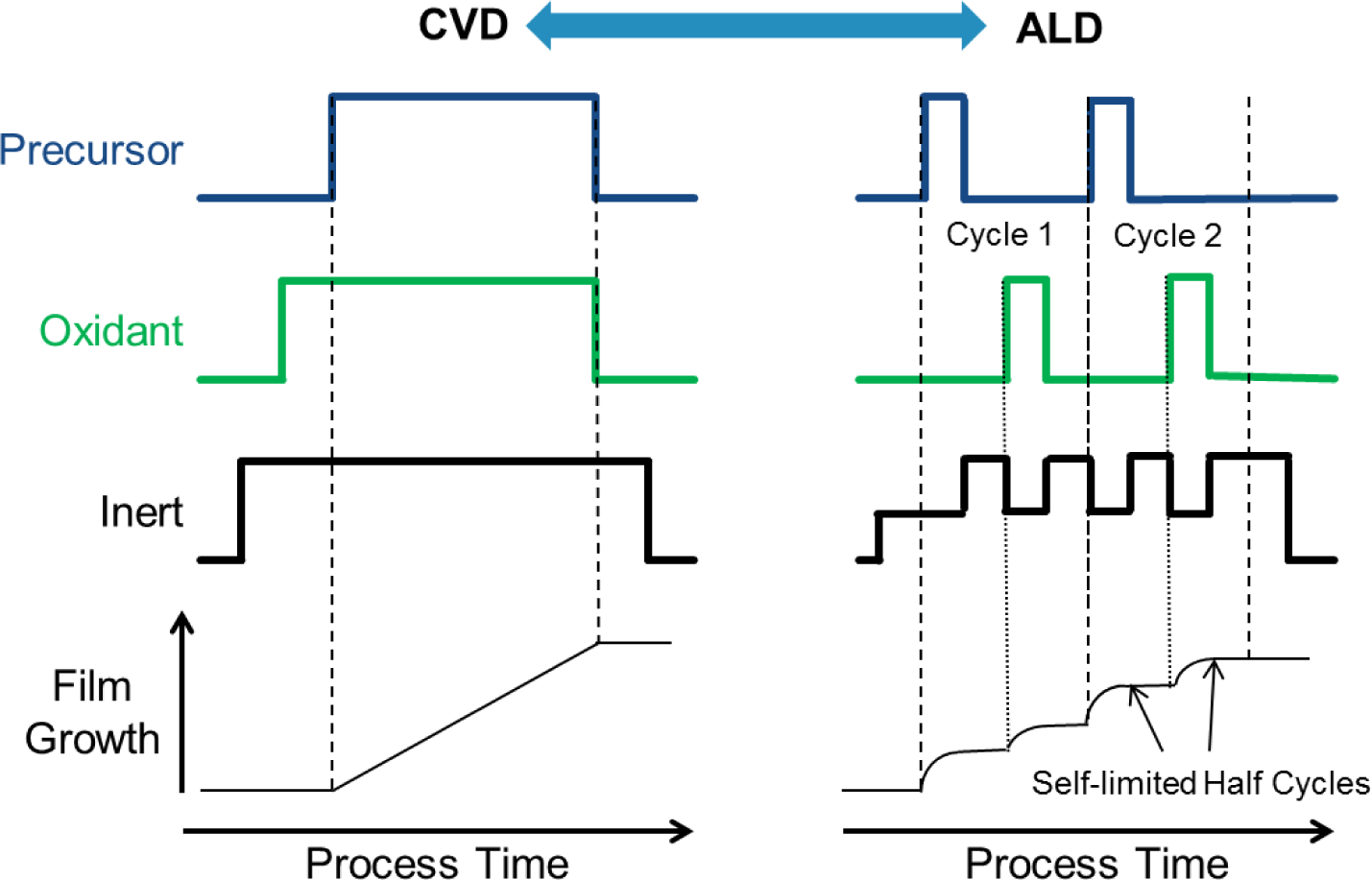


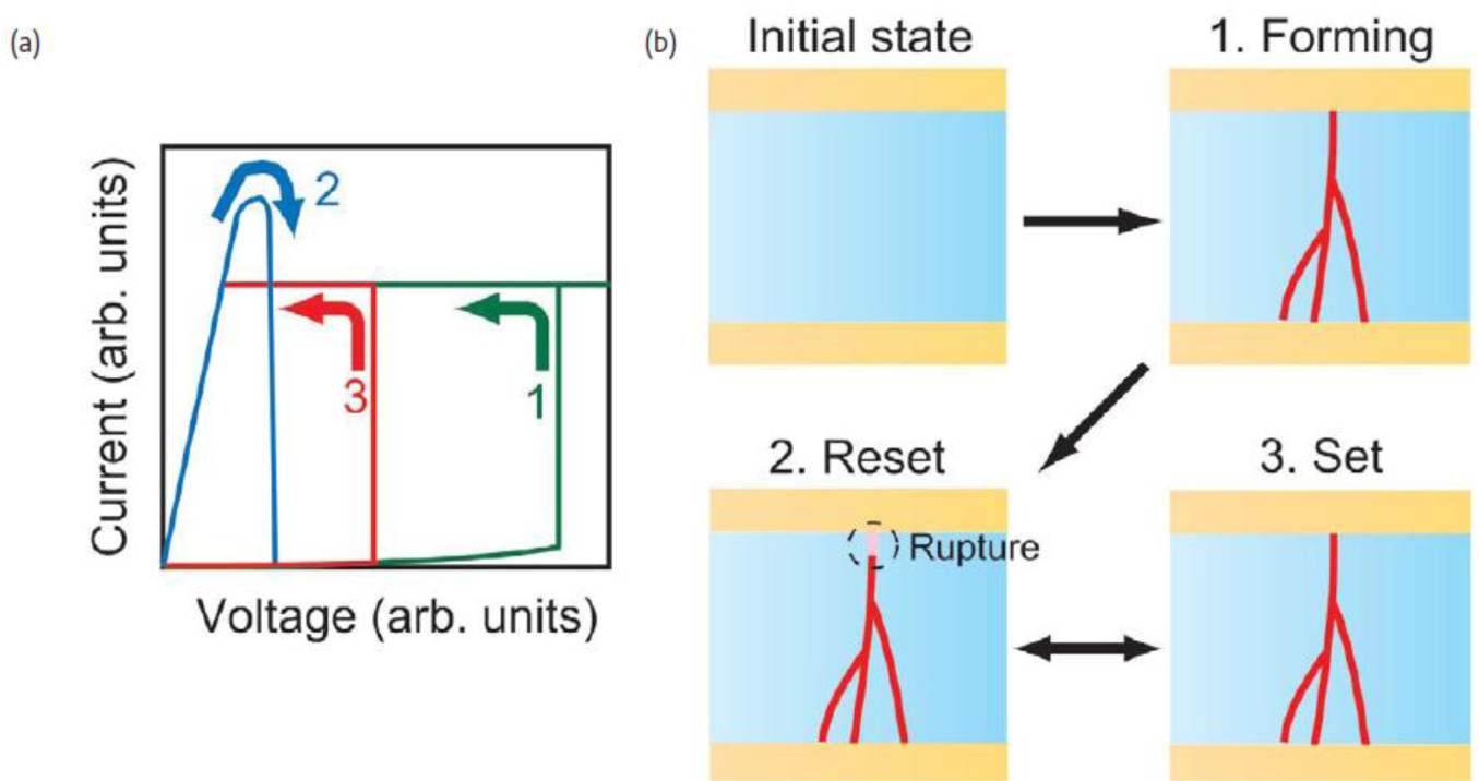


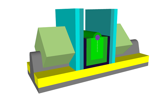
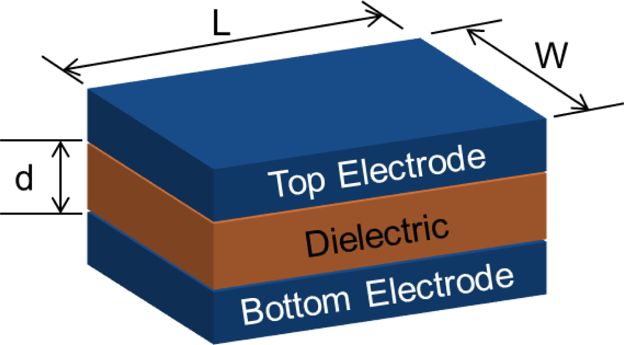
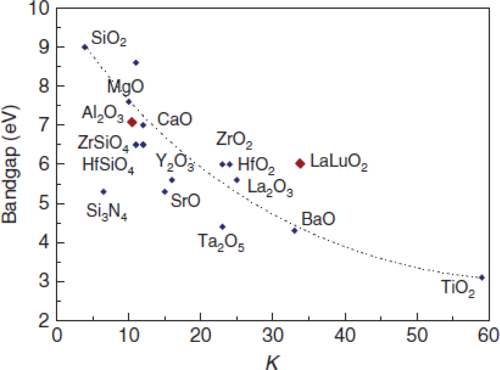
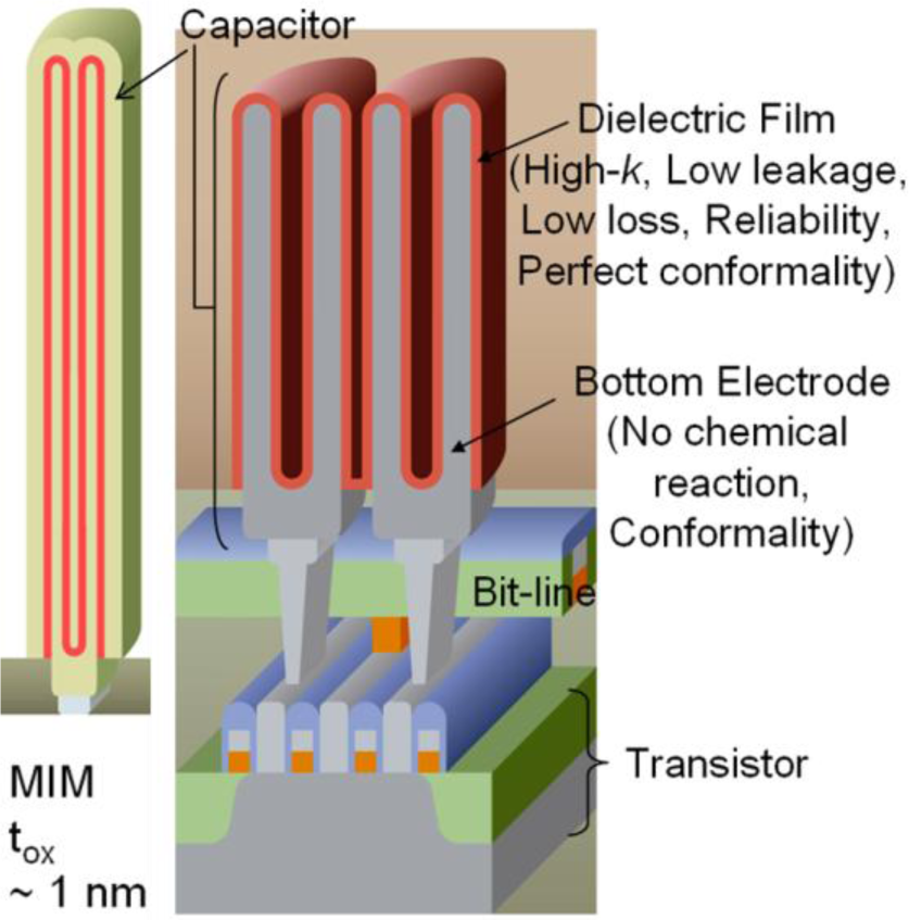
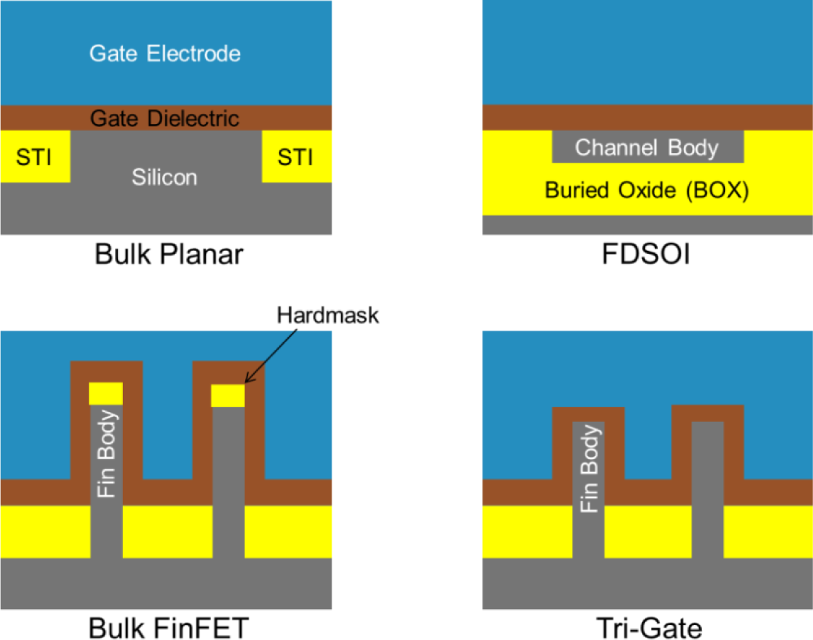
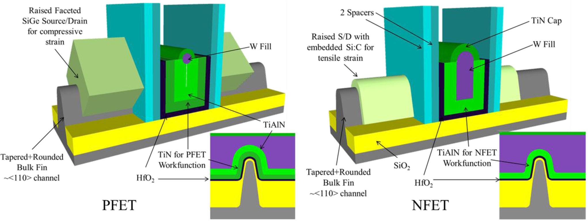
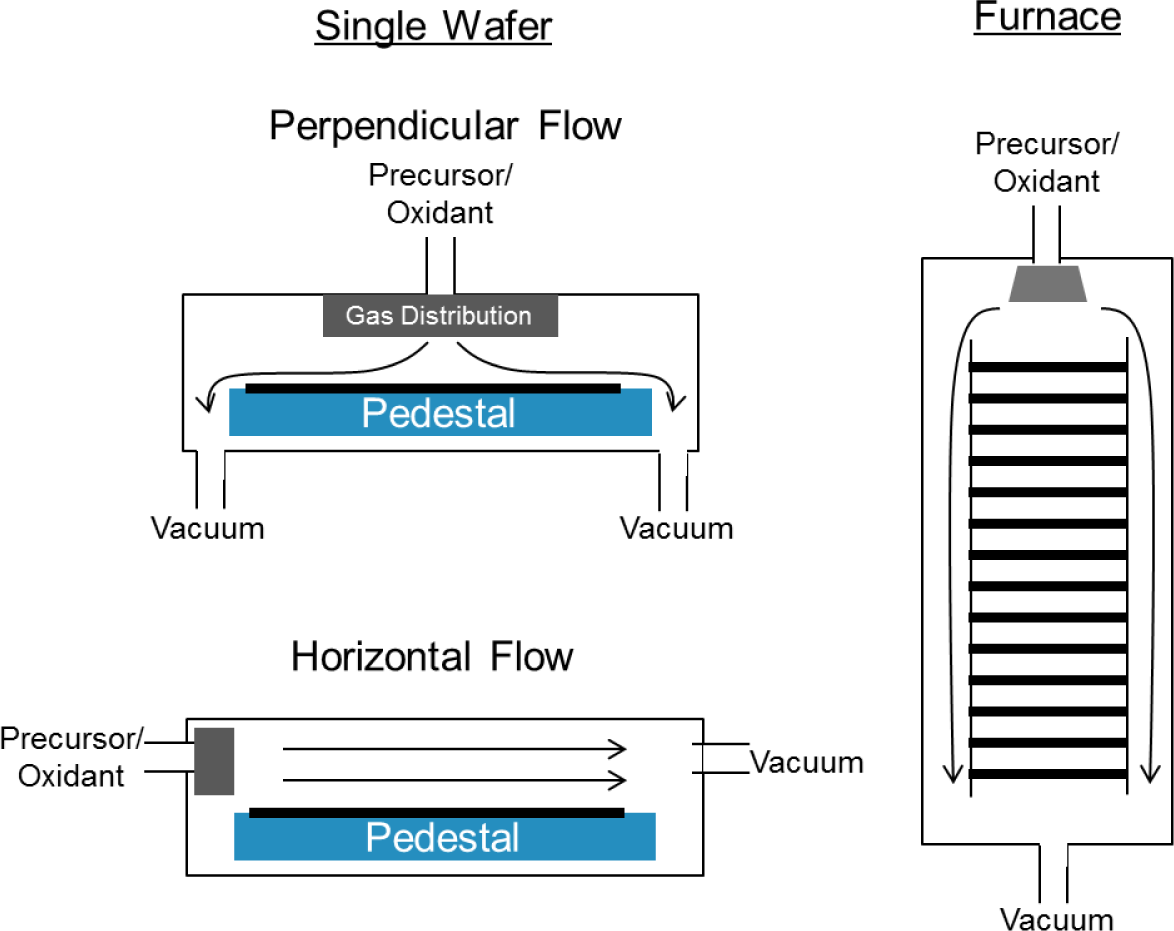
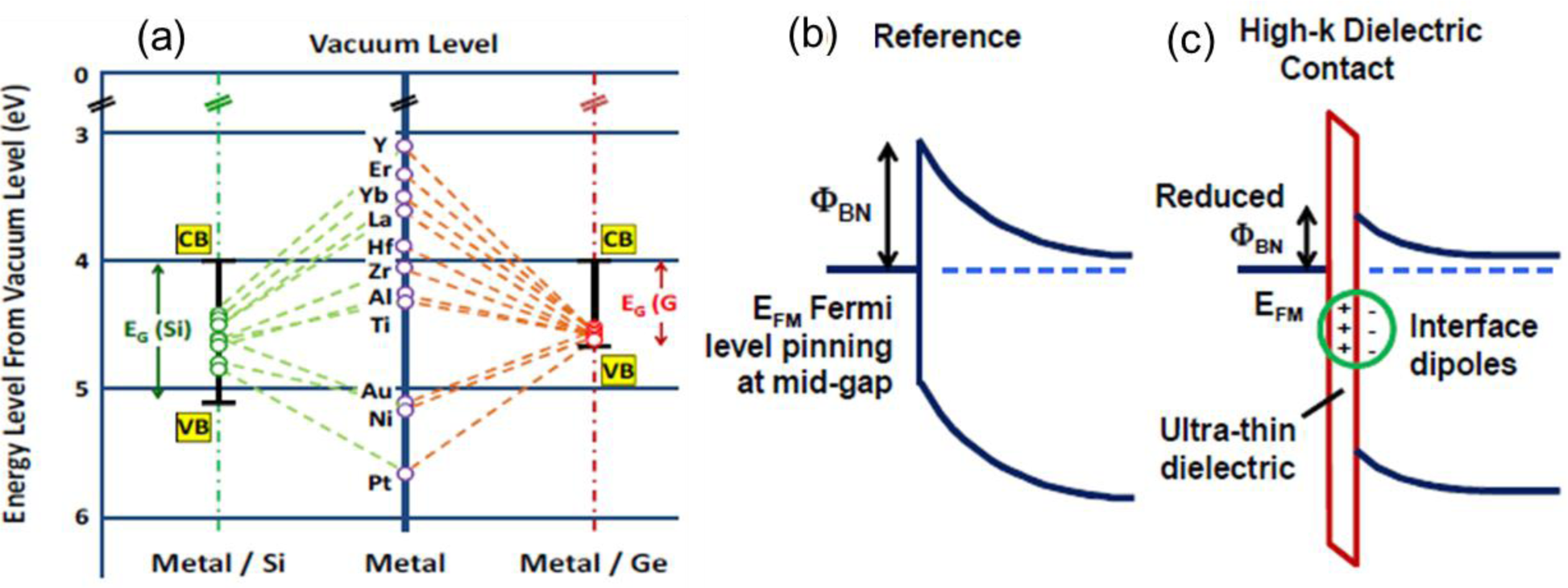
| Technology and Node | CGP * (nm) | Fin Pitch (nm) | L (nm) | N/P DIBL (mV/V) | N/P SS (mV/dec) | N/P Ion (mA/μm) By Weff ** | N/P Ion (mA/μm) By Device Footprint | N/P Ion (nA) per Fin |
|---|---|---|---|---|---|---|---|---|
| Intel 22 nm Tri-Gate | 90 | 60 | 30 | ~50 | 71/72 | 0.88/0.74 # | 1.08/0.91 | 65/55 |
| TSMC 16 nm FinFET | 64 | 48 | 30 | 52/42 | 73/71 | – | 0.94/0.98 ## | 45/47 |
| STMicro 14 nm FDSOI | 100 | N/A | 20 | 73/85 | 90/97 | 0.86/0.82 | 0.86/0.82 | – |
*Contacted Gate Pitch (CGP);#See Table 1 in [24];**Effective device width (Weff) is the linear channel width;##Estimated based on reported Ion/Ioff.
© 2014 by the authors; licensee MDPI, Basel, Switzerland This article is an open access article distributed under the terms and conditions of the Creative Commons Attribution license (http://creativecommons.org/licenses/by/3.0/).
Share and Cite
Clark, R.D. Emerging Applications for High K Materials in VLSI Technology. Materials 2014, 7, 2913-2944. https://doi.org/10.3390/ma7042913
Clark RD. Emerging Applications for High K Materials in VLSI Technology. Materials. 2014; 7(4):2913-2944. https://doi.org/10.3390/ma7042913
Chicago/Turabian StyleClark, Robert D. 2014. "Emerging Applications for High K Materials in VLSI Technology" Materials 7, no. 4: 2913-2944. https://doi.org/10.3390/ma7042913