Article

Temperature-Driven Structural and Morphological Evolution of Zinc Oxide Nano-Coalesced Microstructures and Its Defect-Related Photoluminescence Properties

1
Materials Science Program, School of Applied Physics, Faculty of Science and Technology, Universiti Kebangsaan Malaysia, Selangor Darul Ehsan 43600, Malaysia
2
Technical Support Division, Malaysian Nuclear Agency, Kajang 43000, Malaysia
3
Low Dimensional Materials Research Centre, Department of Physics, Faculty of Science, University of Malaya, Kuala Lumpur 50603, Malaysia
*
Authors to whom correspondence should be addressed.
These authors contributed equally to this work.
Materials 2016, 9(4), 300; https://doi.org/10.3390/ma9040300
Submission received: 4 January 2016 / Revised: 19 March 2016 / Accepted: 15 April 2016 / Published: 20 April 2016
(This article belongs to the Section Advanced Materials Characterization)

Abstract

:
In this paper, we address the synthesis of nano-coalesced microstructured zinc oxide thin films via a simple thermal evaporation process. The role of synthesis temperature on the structural, morphological, and optical properties of the prepared zinc oxide samples was deeply investigated. The obtained photoluminescence and X-ray photoelectron spectroscopy outcomes will be used to discuss the surface structure defects of the prepared samples. The results indicated that the prepared samples are polycrystalline in nature, and the sample prepared at 700 °C revealed a tremendously c-axis oriented zinc oxide. The temperature-driven morphological evolution of the zinc oxide nano-coalesced microstructures was perceived, resulting in transformation of quasi-mountain chain-like to pyramidal textured zinc oxide with increasing the synthesis temperature. The results also impart that the sample prepared at 500 °C shows a higher percentage of the zinc interstitial and oxygen vacancies. Furthermore, the intensity of the photoluminescence emission in the ultraviolet region was enhanced as the heating temperature increased from 500 °C to 700 °C. Lastly, the growth mechanism of the zinc oxide nano-coalesced microstructures is discussed according to the reaction conditions.

1. Introduction

Zinc oxide (ZnO) has been widely studied and has received noteworthy attention since 1935 [1], as our daily lives and current industries crucially rely on this compound. It has been recognized as one of the well-known potential materials that could be beneficial and serviceable for electronic and optoelectronic applications owing to its attractive properties. For instance, ZnO has a direct and wide band gap energy of 3.37 eV, which enables it to be transparent in visible light and to operate in the ultraviolet (UV) and blue wavelength regions [2]. Moreover, ZnO has a large exciton binding energy of approximately 60 meV that ensures an efficient excitonic emission at room temperature, enabling it to be suitable for UV optoelectronic applications [3]. This notable exciton binding energy of ZnO makes it a more attractive material than other compounds, especially GaN, a compound with exciton binding energy of 26 meV. A number of methods have been reported in the literature regarding the synthesis of ZnO materials with a range of different morphologies, such as thermal evaporation [4,5], carbothermal reduction [6], magnetron sputtering [7], cathodic electrodeposition [8,9], hydrothermal synthesis [10,11], and sol-gel processing [12,13]. However, the thermal evaporation approach remains as a valuable technique and can be interpreted as a cost effectiveness technology for the growth of metal oxide micro- or nanostructures. There is little research reporting the achievability of growing ZnO at comparatively low temperature utilizing the liquid phase growth methods such as hydrothermal synthesis and sol-gel processing. However, there are some drawbacks relating to these processes in contrast to the thermal evaporation method, such as: (i) these methods demanded additional fabrication step, for example furnishing a seed layer by physical methods prior to the actual synthesis [14]; (ii) these methods required a precise control of the composition, pH, and also concentration of an electrolyte solution; (iii) the growth rate of these methods was inferior to the vapor phase process [15]; and (iv) these methods needed a post thermal annealing treatment to alter the thin film’s internal crystallization and concurrently reduced the defects in the thin film and then prevented the growth of other crystalline phases [16].
Miscellaneous factors have been defined from the thermal evaporation method that leads to the formation of ZnO with contrastive morphologies and properties. However, not all the factors are of requisite. Temperature is the key parameter, which ought to be contemplated for the formation of diverse ZnO morphologies before employing it in various applications. Several research groups have deliberated the dependency of temperature and luminescence properties of ZnO [17,18,19]. However, they have added graphite powder as a catalyst in their experiments and run at source temperature up to the 950 °C. In particular, the presence of a catalyst in the fabrication is not only detrimental to the intrinsic properties of the materials but also deleterious to its final product applications due to the existing contamination. Using an extreme temperature to locally heat the reactant source in order to enable the vaporization will restrict the fabrication of ZnO micro and nanomaterials in gentle circumstances [20,21]. Furthermore, Lee [22] reported that luminescent property, morphology, and microstructure of ZnO nanostructures are related to the oxidation rate of Zn film. Very recently, Yuan et al. [23] studied the dependence of different oxidation temperatures on the growth morphologies and microstructure of ZnO. However, they did not study the luminescence properties.
The photoluminescence (PL) of ZnO have been comprehensively studied. It is the spontaneous emission of light from a material following an optical emission. The motivation of PL studies is to elucidate the correlative between the origins of different emission bands to the origins of different ZnO defect emissions [24]. Typically, ZnO exhibits a near band edge UV emission and a broad defect-related visible emission. This visible emission is often described in green luminescence, although violet, blue, yellow, and orange-red luminescence have also been reported [25,26]. Nevertheless, the understanding of ZnO defects by PL principle is still inadequate and remains controversial.
Here, we report the synthesis of ZnO nano-coalesced microstructures with varied morphologies via thermal evaporation without any metal catalyst or pre-deposited ZnO seed layer at 500 °C, 600 °C, and 700 °C, respectively. We comprehensively studied the connection between the surface structure defects with PL and XPS spectra as other researchers did not focus on this. Under this circumstance, results from the XPS spectra will be used to support the PL analysis so that a better prediction and dissection regarding to the origins of surface structure defects can be derived in this study. The inherent factors primarily influencing the material properties and growth mechanism will be explored as well.

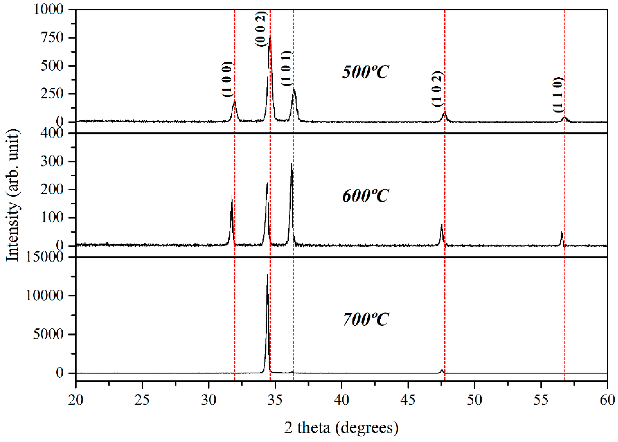
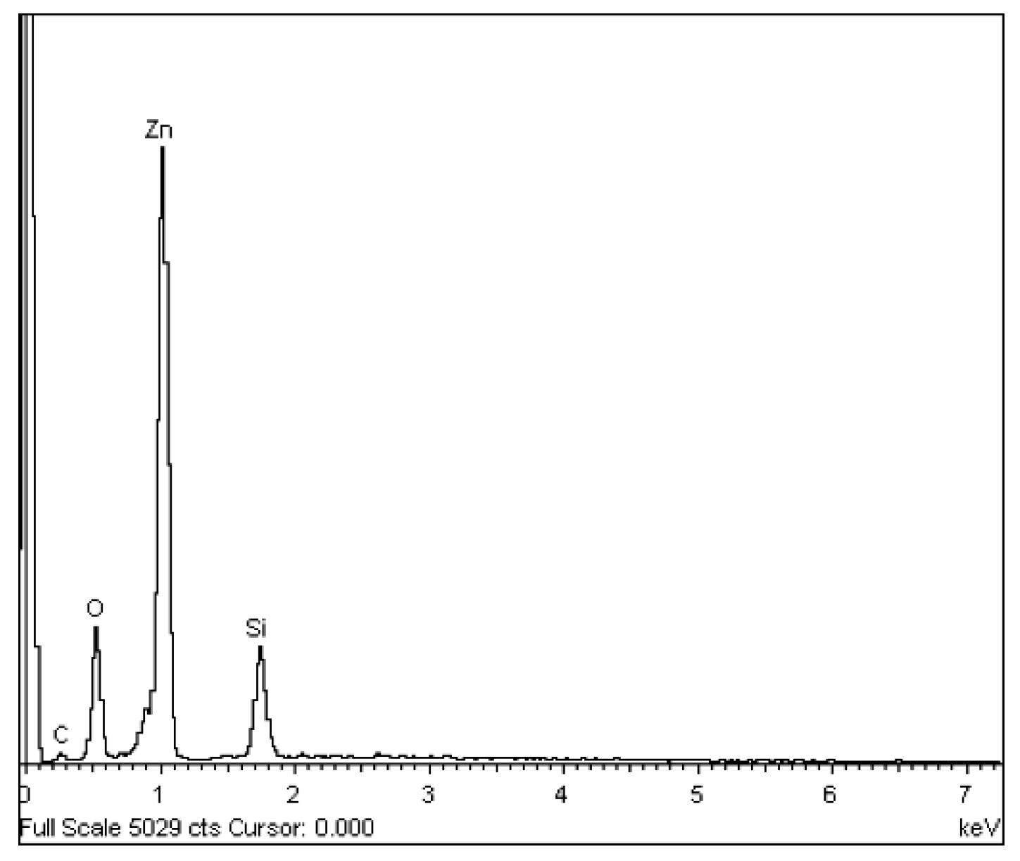
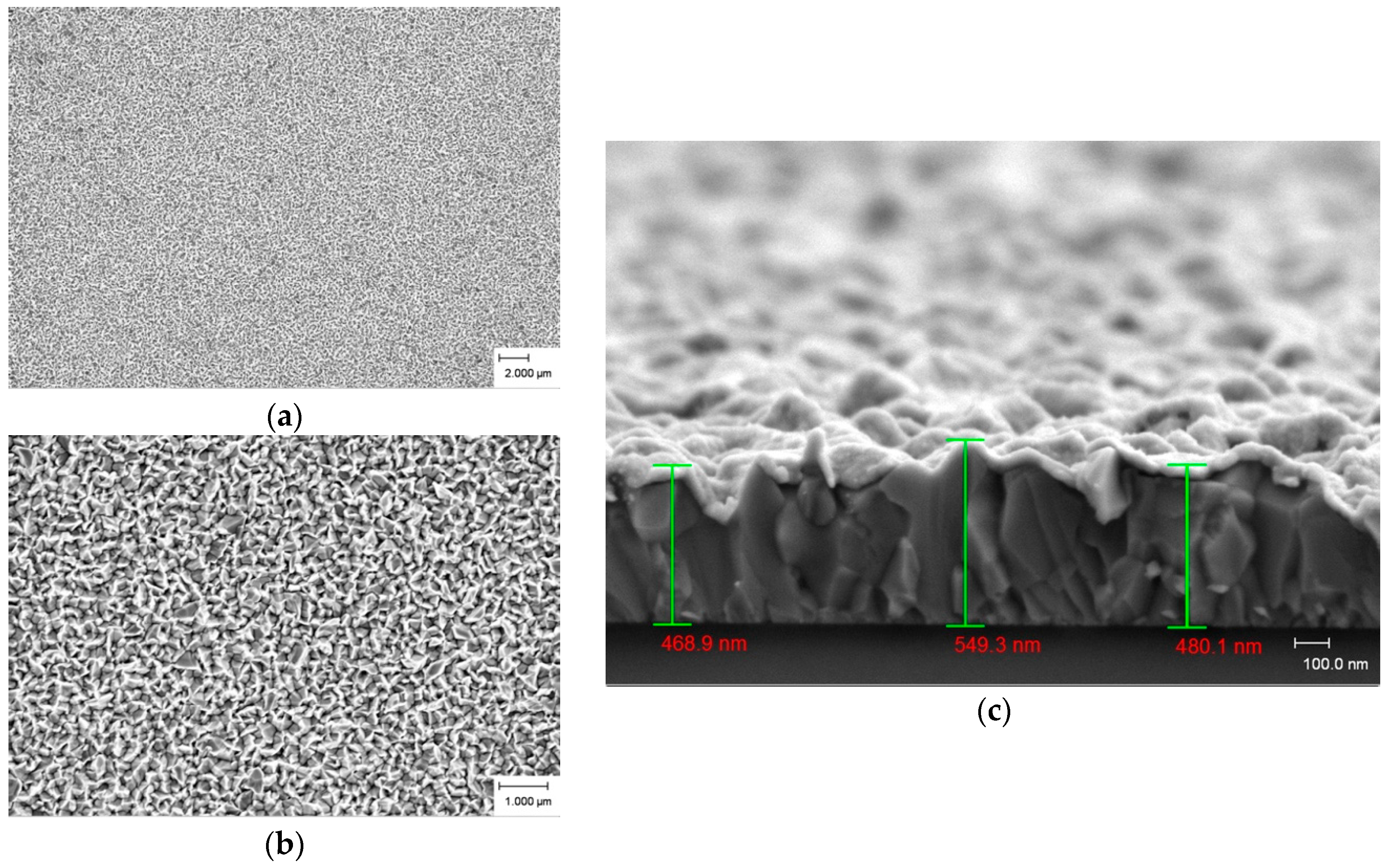
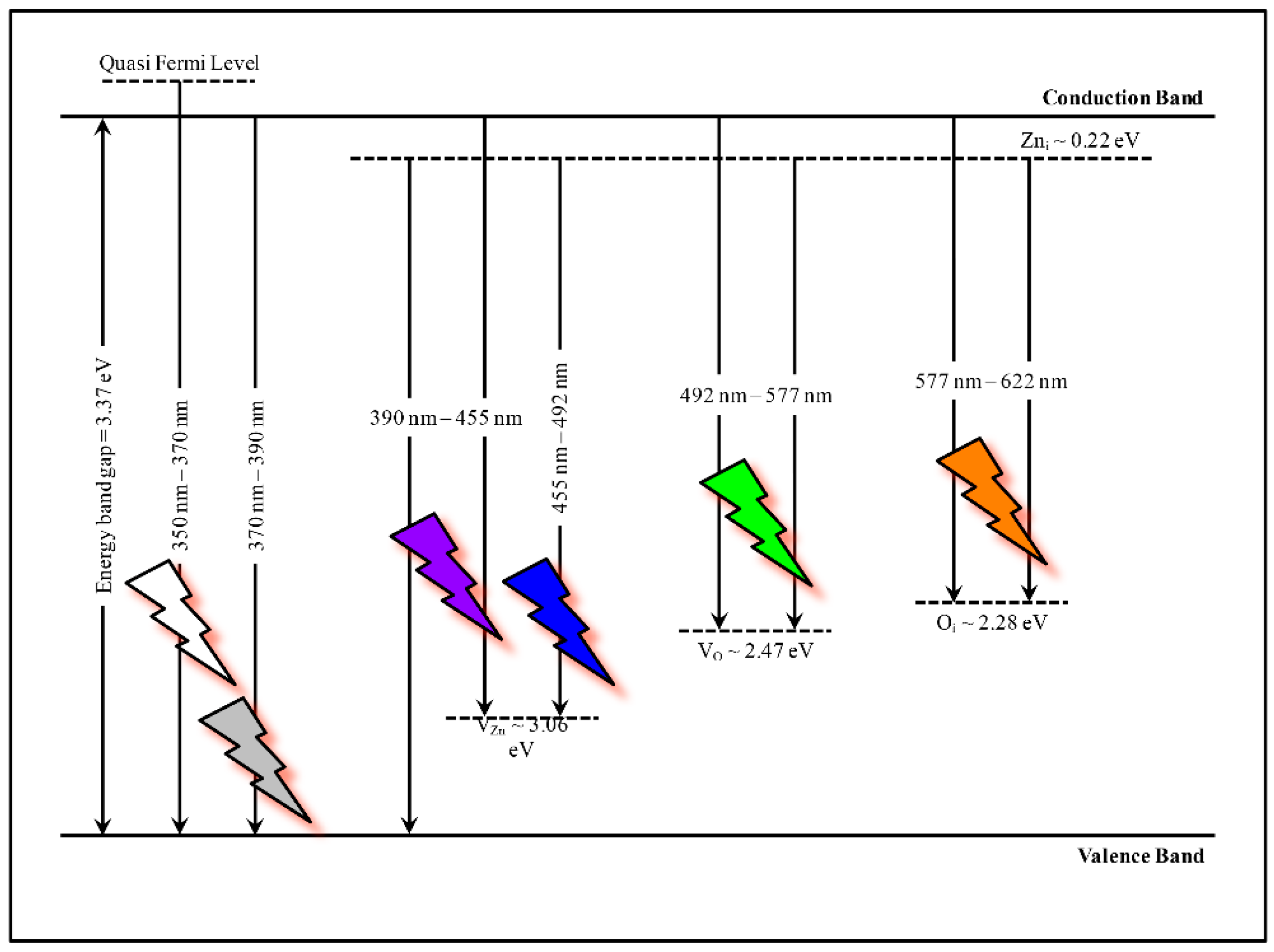
2. Results and Discussion

The XRD patterns of the deposited ZnO samples on SiO2-coated Si substrates at different growth temperatures are illustrated in Figure 1.
The XRD diffraction peaks can be assigned to (100), (002), (101), (102), and (110) hexagonal wurtzite structures of ZnO, with the cell parameter of a = b = 3.242 Å and c = 5.188 Å according to the JCPDS card no. 01-079-0205. The diffraction peak at a Bragg angle of around 34.5°, corresponding to the (002) plane overwhelmingly reveals the preferred orientation of ZnO growth at 500 °C and also 700 °C. This close-packed plane is predictably dominant for ZnO, as it has the lowest surface energy among the possible orientations of hexagonal wurtzite ZnO [22,27]. However, ZnO grown at 600 °C has a preferred orientation along the (101) plane, compared to the ones on 500 °C and 700 °C. This unfavorable crystal plane appears to be related to the oxidation rate, which leads to inclusion of the absorbed oxygen atoms in the ZnO lattice [22]. Thus, with the increase in oxidation temperature, the ZnO should present preferential growth in the (101) orientation. However, our XRD results are in contrast with this statement. The XRD peak intensity is related to many factors, which comprise the crystallization quality, density, and also thickness of thin films. Shifting of preferred orientation from the (002) to (101) plane for 600 °C sample is predominantly due to the dissimilarity of these factors. As shown in Figure 3, Figure 4 and Figure 5, numerous ZnO-branched nanowires (Figure 4) are formed on the substrate surface prepared at 600 °C compared to the quasi-mountain chain-like ZnO (Figure 3) and pyramidal textured ZnO (Figure 5) obtained at 500 °C and 700 °C, respectively. It is suggested that the strong (101) peak can be ascribed to the ZnO-branched nanowires formed with high density and also a different dimensional structure. The intensity of the (101) peak appears to reflect the density of ZnO-branched nanowires, which is identical as reported by other researchers [22,28]. No peaks for the unreacted metallic zinc and no other impurities were detected confirming the full conversion of the zinc metal to ZnO and the high purity of the obtained products.
A representative EDX spectrum presented in Figure 2 depicts a Si-related peak, which originated from the substrate, while the C peak is caused by the carbon contamination. Carbon deposits occur due to the interaction of the electron beam with the hydrocarbon molecule vapors that exist in the vacuum chamber or on the substrate surface [29]. Moreover, only zinc and oxygen atoms are seen in the EDX spectrum, proving the obtainment of pure ZnO products, which was also confirmed through XRD spectrum. The quantitative EDX analysis indicated that the oxygen content was intense than the zinc. However, the atomic composition ratio of oxygen to zinc could not be quantified, as a portion of the oxygen originated from the SiO2-coated Si substrate.
The FESEM images of the ZnO as-deposited products with different growth temperatures in the plan view (low and high magnification) and cross section are presented in Figure 3, Figure 4 and Figure 5. Figure 3a,b show a dense, multi-directional, and irregular shaped quasi-mountain chain-like ZnO structure growth at 500 °C. Dimensions are difficult to measure as a consequence of these structures’ growth in 3D prism- and pyramid-like form with an irregular base. From the cross-section view (Figure 3c), we noticed a continuous powdery thin ZnO layer grown above a close-packed ZnO structure. The overall thickness of the quasi-mountain chain-like ZnO thin film ranges from 460 nm to 550 nm.
Figure 4a,b illustrate ZnO-branched nanowire growth from an agglomeration nucleus at 600 °C. These microstructures grew uniformly and decreased gradually like a needle at the end, with a diameter of about 40 nm to 250 nm and a length of more than 1 μm. From Figure 4c, we can clearly see some ZnO-branched hexagonal structures with sharp tip growth at the end of the branched nanowires. The thickness for ZnO-branched nanowire structure thin film is around 44 μm.
Figure 5a,b elucidate an irregular base of pyramidal textured ZnO structures obtained at 700 °C. Some of these structures display a small flat hexagonal facet at the top and some indicate sharp tips at the end. From the cross section view (Figure 5c), we observed that granular ZnO was deposited on the dense structure. The thickness of this thin film is in the range of 3.3 μm to 3.7 μm. It should be noted that the pyramidal ZnO textured structures obtained at 700 °C were densely packed, which results in the dominant diffraction peak of the (002) phase in the XRD results.
Growth temperature is a critical experimental parameter, which determines the kinetic energy for the formation of different morphologies of ZnO. It has an impact on the quantity of the reactive vapor to be generated and the surface diffusion length of the absorbed vapor types [30]. Temperature may facilitate various degrees of supersaturation of ZnO in its gaseous state, resulting in different structures [31]. At high temperature of 700 °C, more Zn or Zn suboxide vapors were produced to form a thick film. Whereas at a moderate temperature of 600 °C, the vaporization rate of Zn or Zn suboxides was lower than that at 700 °C. This means the exhaustion of gaseous product was slower at sintering temperature of 600 °C than at 700 °C. Hence, a thicker film was formed. In the case of 500 °C, only some Zn or Zn suboxides was formed, so that the thickness of film reduced dramatically. Vapor-solid (VS) and vapor-liquid-solid (VLS) processes are always used to describe the growth mechanism of ZnO micro and nanostructures. The VLS model is usually used to explain the growth mechanism at high temperatures, while the VS model dominates at low temperatures [32]. However, we have different views on this point. Based on our opinion, the VS model is more suitable and fulfills our sample growth mechanism since no “catalyst ball” is found in the tips of the structures but there is a reduction in dimensions of the samples.
The chemical states of the prepared ZnO were investigated by the XPS measurements. The wide scan spectrum of the sample prepared at 500 °C is depicted in Figure 6. Here, the typical ZnO XPS spectrum can be seen. The mean peaks are carbon, oxygen, and Zn.
The carbon peak at the binding energy of 284.5 eV originates from the sample surface because of its contamination, and is used for the internal calibration of the system [33]. For further information about the regions of interest above, a narrow and high-resolution scan was employed for the elements. Figure 7 and Figure 8 depicted the narrow scan of the oxygen 1s and Zn 2p3/2 for the samples prepared at 500 °C, 600 °C, and 700 °C, respectively.
The deconvoluted oxygen 1s XPS spectra (using the XPS peak fit software) of prepared samples shown in Figure 7 reveals the oxygen ions (O2−) in the wurtzite structure of hexagonal ZnO at 529 eV, whereas the peaks at 530 eV and 531 eV are attributed to the O2− in oxygen-deficient regions (oxygen vacancies or defects) and O2 species (chemisorbed or dissociated oxygen), respectively [34,35,36,37]. The difference of each deconvoluted peak reveals the significant weight of each component of the oxygen 1s. Further, the Zn 2p3/2 peak at binding energy of 1021 eV can be deconvoluted to two components, the 1020 eV belonging to pure Zn (Zn interstitial) and the 1021 eV depicted to the Zn–O in the ZnO crystal [33,38,39]. Based on the rules of quantitative analysis of the XPS spectrum, the relative atomic surface concentrations of elements can be determined using the integrated area under principal peaks and a formula for quantification [33,40] as follows:
C x   =   I x / S x i   = 1 I x / S x ,
where Cx is the atomic concentration of element x, Ix is the integral intensity in Gaussian fitted XPS spectrum of element x, and Sx is the relative sensitivity factor for element x based on the spectroscopy used. The relative atomic concentration of each component is shown in Table 1.
From the results, it can be deduced that the prepared ZnO contains Zn interstitial and oxygen vacancies, and the relative atomic concentration percentage of Zn interstitial and oxygen vacancies was the highest in the sample prepared at 500 °C. It is clear that at higher temperatures more reactions of Zn and O result.
Figure 9 presents the room temperature PL spectra filters by Schott glass filter with 330 nm cut-off wavelengths for the prepared ZnO at different growth temperatures.
The Gaussian deconvoluted spectra exhibit multi emission traps in the UV range from 350 nm to 370 nm and from 370 nm to 390 nm. These multi emission traps (blue lines) can be overlapped and combined to form a prominent peak (red dot line), which can be seen in Figure 9. The former range emission can be associated with the interband transition of the photogenerated electrons and holes. Relatively, a considerably stronger irradiation of excitation light will create a quasi Fermi level inside the conduction band. Therefore, the recombination of electron-hole pairs from this level to valence band will emit a photon energy that is greater than the ZnO energy band gap (3.37 eV) [41,42]. The latter range emission dovetails to the near band edge emission, which arises from the recombination of free excitons through an exciton-exciton collision process. The width of the UV emission indicates that the peak consists of sundry emissions. The emissions can be assigned to the two-phonon replicas due to the two transverse optical phonons within a range of separation from 50 meV to 110 meV [22]. The PL spectra also revealed a broad range of visible emission. Several defect-related recombination centers, such as Zn vacancy (VZn), oxygen vacancy (VO), interstitial Zn (Zni), interstitial oxygen (Oi), Zn antisite (ZnO), and oxygen antisite (OZn) defects were responsible for the luminescence process of ZnO in the visible region of electromagnetic radiation [43]. Among the defects, ZnO, is unlikely to be stabilized under equilibrium conditions ascribed to their high formation energies. Additionally, Zni and VO can yield free electrons (donor type defects), whereas VZn, Oi, and OZn consume free electrons (acceptor type defects) in a ZnO crystal. The relative content of donors and acceptors determines the semiconductive property and further semiconductor-related properties of ZnO [44,45]. The observed PL spectra revealed emission band at 390 nm to 455 nm (violet luminescence) is probably attributed to the radiative defects related to the interface traps existing at the grain boundaries and emitted from the radiative transition between this level and the valence band [46]. The band from 455 nm to 492 nm (blue luminescence) is due to the single ionized VZn [47], while the band from 492 nm to 577 nm (green luminescence) is commonly referred to as a deep-level or a trap-state emission attributed to the single ionized VO and the emission results from the radiative recombination of a photogenerated hole with an electron occupying the VO [48]. Furthermore, the band from 577 nm to 622 nm (yellow-orange luminescence) is attributed to the transition from the bottom of the conduction band to the Oi [49].
Theoretically, the positions of these bands have been predicted. This can be explained by the full potential linear muffin-tin orbital method, which explains that the positions of the Zni, VZn, VO, and Oi are located at 0.22 eV, 3.06 eV, 2.47 eV, and 2.28 eV below the conduction band, respectively [50]. A detailed schematic energy level diagram of various level emissions in ZnO has been illustrated in Figure 10, which gives a vision for the recombination of electron-hole pairs from various defects back to the valence band and then emits photon energy, which fully supports our previous PL explanation.
The origin of the ZnO PL emission is a complicated process, as it is most related to the oxygen vacancies and/or Zn interstitial. Furthermore, it is a difficult task to correlate the PL emissions with optical transitions. Thus, PL emissions from ZnO defect energy levels are extremely complex and still not fully understood. However, the results from the XPS and PL support each other. From Figure 7 and Figure 8 it can be shown that the raw area of oxygen vacancies and Zn interstitial (bolded and italicized) from the respective total raw area decreases as the temperature increases. Also, the relative intensity of the UV near band edge emission to the visible emission from the PL results (Figure 9) increases as the temperature increases, which point to the improvement of ZnO quality. Consequently, the results indicated that the sample prepared at 500 °C has a higher percentage of oxygen vacancies and also Zn interstitial. In addition, the percentage of oxygen vacancies and Zn interstitial were enhanced as the temperature increased.

3. Materials and Methods

Cleaved single polished appearance SiO2-coated Si substrates with dimensions of 12 × 12 mm2 were used as the ZnO film growth medium. Prior to the growth, the substrates were ultrasonically cleaned sequentially with the acetone, methanol, and isopropyl alcohol, sonicated for 15 min in each respective solvent, and followed by a rinse with deionized water. The cleaned substrates were dried in a stream of air and underwent a dehydration bake in an oven at 100 °C to remove the trapped and absorbed moisture from the substrate surface. The growth process was carried out by the thermal evaporation method in a conventional commercial horizontal three-zone temperature alumina tube furnace. Metallic zinc powder (Emsure® grade; particle size <45 nm; Merck KGAa, Darmstadt, Germany) of approximately 1.50 g was dispersed evenly in a rectangular alumina boat in the absence of any catalyst. The boat was loaded into the center of the tube of the horizontal furnace afterwards with the substrate located above the source at an estimated vertical distance of 15 mm with the single polished surface facing downward. As the temperature began to rise from room temperature with a program ramp rate of 10 °C/min, high purity argon gas was purged into the tube throughout the heating process with a flow rate of 800 sccm, providing a shield against environmental contamination. The flow of argon gas was stopped immediately once the temperature reached 419 °C (melting point of zinc), and the heating process was continuous done until it achieved the desired temperature of 500 °C, 600 °C, and 700 °C, respectively. A mixture of 1.6% oxygen and 98.4% argon as a reactant gas flowed throughout the tube maintaining the temperature for 30 min. The ZnO as-deposited product was allowed to cool inside the sealed tube furnace to room temperature naturally after a 15 min flow of argon gas in order to substitute the entire oxygen gas residue inside the tube.
The surface morphologies of the ZnO structures were examined using field emission scanning electron microscopy (FESEM, Carl Zeiss Supra 55VP, Jena, Germany) coupled an energy dispersive X-ray capability (EDX, Oxford Inca, Abingdon, UK) to quantify the elemental compositions. A glazing incidence X-ray diffractometer (XRD, Bruker D8 Advance, Karlsruhe, Germany) using copper-monochromatized Cu Kα1 radiation (λ = 0.154 nm) with an accelerating voltage of 40 kV and a current of 40 mA was used to determine the phase structures. The diffractograms were recorded in the 2θ range of 20° to 60° with a controlled step size of 0.025°. The surface compositions of the as-deposited products were analyzed by XPS (Kratos Axis Ultra DLD, Manchester, UK). Binding energies were corrected for the charge shift using the C 1s peak of carbon (BE = 284.5 eV) as a reference [37]. For the optical emission measurements, the PL spectra were recorded using a filter spectrofluorometer (Edinburgh Photonics, model FLSP 920, Livingston, UK) as an excitation source. The PL spectra were measured in the range of 350 nm to 630 nm with a 325 nm excitation wavelength at room temperature.

4. Conclusions

In summary, the nano-coalesced microstructured ZnO thin films were prepared via a thermal evaporation approach. The starting temperatures varied from 500 °C to 700 °C with the flow of oxygen and argon gas mixture. The results show enhancements on structural and optical properties of the contrastive ZnO morphologies. The near band edge UV emission of the prepared ZnO samples was enhanced with the temperature. Connection between the surface structure defects with PL and XPS spectra have been proven. Based on the obtained results, the growth mechanism of ZnO nano-coalesced microstructures was built up and discussed.

Acknowledgments

The authors gratefully acknowledge use of the services and research facilities provided by the Centre of Research and Instrumentation Management, Universiti Kebangsaan Malaysia. The authors also express their sincere thanks for the financial support funded by the authorities of University through the short-term grant number DIP-2014-023 and the Ministry of Higher Education Malaysia through the MyBrain15.

Author Contributions

Karkeng Lim, Muhammad Azmi Abdul Hamid, Roslinda Shamsudin, and N.H. Al-Hardan contributed equally to this work with conceived and designed the experiments; Karkeng Lim performed the experiments, analyzed the data, and drafted the manuscript; Muhammad Azmi Abdul Hamid and Roslinda Shamsudin revised and proved that the draft manuscript; N.H. Al-Hardan, Ishak Mansor, and Weesiong Chiu gave technical support and conceptual advice.

Conflicts of Interest

The authors declare no conflict of interest.

References

  1. Bunn, C.W. The lattice dimensions of zinc oxide. Proc. Phys. Soc. 1935, 47, 835–842. [Google Scholar] [CrossRef]
  2. Jagadish, C.; Pearton, S.J. Zinc Oxide Bulk, Thin Films and Nanostructures: Processing, Properties and Applications; Elsevier Ltd.: Hong Kong, China, 2006; pp. 1–21. [Google Scholar]
  3. Aneesh, P.M.; Kalarikkal, N. ZnO nanostructures and its luminescent properties. In Advanced Nanomaterials: Synthesis, Properties and Applications; Thomas, S., Kalarikkal, N., Stephen, A.M., Raneesh, B., Haghi, A.K., Eds.; Apple Academic Press Inc.: Oakville, ON, Canada, 2014; pp. 117–148. [Google Scholar]
  4. Abdulgafour, H.I.; Hassan, Z.; Al-Hardan, N.; Yan, F.K. Growth of zinc oxide nanoflowers by thermal evaporation method. Phys. B Condens. Matter. 2010, 405, 2570–2572. [Google Scholar] [CrossRef]
  5. Umar, A.; Suh, E.K.; Hahn, Y.B. Non-catalytic growth of high-aspect ratio ZnO nanowires by thermal evaporation. Solid State Commun. 2006, 139, 447–451. [Google Scholar] [CrossRef]
  6. Lim, Y.S.; Park, J.W.; Kim, M.S.; Kim, J. Effect of carbon source on the carbothermal reduction for the fabrication of ZnO nanostructure. Appl. Surf. Sci. 2006, 253, 1601–1605. [Google Scholar] [CrossRef]
  7. Ellmer, K. Magnetron sputtering of transparent conductive zinc oxide: Relation between the sputtering parameters and the electronic properties. J. Phys. D Appl. Phys. 2000, 33, 17–32. [Google Scholar] [CrossRef]
  8. Yoshida, T.; Komatsu, D.; Shimokawa, N.; Minoura, H. Mechanism of cathodic electrodeposition of zinc oxide thin films from aqueous zinc nitrate baths. Thin Solid Films 2004, 451, 166–169. [Google Scholar] [CrossRef]
  9. Al-Hardan, N.H.; Abdul Hamid, M.A.; Jalar, A.; Lim, K.K.; Shamsudin, R.; Majlis, B.Y. Bi-structure ZnO prepared via cathodic electrodeposition method. Int. J. Electrochem. Sci. 2013, 8, 2430–2439. [Google Scholar]
  10. Barush, S.; Dutta, H. Hydrothermal growth of ZnO nanostructures. Sci. Technol. Adv. Mater. 2009, 10, 13001–13018. [Google Scholar] [CrossRef]
  11. Djurisic, A.B.; Chen, X.Y.; Leung, Y.H. Recent progress in hydrothermal synthesis of zinc oxide nanomaterials. Recent Pat. Nanotechnol. 2012, 6, 124–134. [Google Scholar] [CrossRef] [PubMed]
  12. Li, H.X.; Wang, L.Y.; Liu, H.; Yang, C.H.; Xu, H.Y.; Li, X.; Cui, H.M. Sol-gel preparation of transparent zinc oxide films with highly preferential crystal orientation. Vacuum 2004, 77, 57–62. [Google Scholar] [CrossRef]
  13. Znaidi, L. Sol-gel-deposited ZnO thin films: A review. Mater. Sci. Eng. B 2010, 174, 18–30. [Google Scholar] [CrossRef]
  14. Amin, G.; Asif, M.H.; Zainelabdin, A.; Zaman, S.; Nur, O.; Willander, M. Influence of pH, precursor concentration, growth time, and temperature on the morphology of ZnO nanostructures grown by the hydrothermal method. J. Nanomater. 2011, 5, 1–5. [Google Scholar] [CrossRef]
  15. Rusli, N.I.; Tanikawa, M.; Mahmood, M.R.; Yasui, K.; Hashim, A.M. Growth of high-density zinc oxide nanorods on porous silicon by thermal evaporation. Materials 2012, 9, 2817–2832. [Google Scholar] [CrossRef]
  16. Chin, H.S.; Chao, L.S. The effect of thermal annealing processes on structural and photoluminescence of Zinc oxide thin film. J. Nanomater. 2013, 2013, 1–8. [Google Scholar] [CrossRef]
  17. Fang, F.; Zhao, D.X.; Zhang, J.Y.; Shen, D.Z.; Lu, Y.M.; Fan, X.W.; Li, B.H.; Wang, X.H. The influence of growth temperature on ZnO nanowires. Mater. Lett. 2008, 62, 1092–1095. [Google Scholar] [CrossRef]
  18. Al-Azri, K.; Nor, R.M.; Amin, Y.M.; Al-Ruqeishi, M.S. Effect of source temperature on the morphology and photoluminescence properties of ZnO nanostructures. Appl. Surf. Sci. 2010, 256, 5957–5960. [Google Scholar] [CrossRef]
  19. Yousefi, R.; Muhamad, M.R.; Zak, A.K. The effect of source temperature on morphological and optical properties of ZnO nanowires grown using a modified thermal evaporation set-up. Curr. Appl. Phys. 2011, 11, 767–770. [Google Scholar] [CrossRef]
  20. Liu, F.; Cao, P.J.; Zhang, H.R.; Sheng, C.M.; Wang, Z.; Li, J.Q.; Gao, H.J. Well-aligned zinc oxide nanorods and nanowires prepared without catalyst. J. Cryst. Growth 2005, 274, 126–131. [Google Scholar] [CrossRef]
  21. Calestani, D.; Zha, M.Z.; Zanotti, L.; Villani, M.; Zappettini, A. Low temperature thermal evaporation growth of aligned ZnO nanorods on ZnO film: A growth mechanism promoted by Zn nanoclusters on polar surfaces. CrystEngComm 2011, 13, 1707–1712. [Google Scholar] [CrossRef]
  22. Lee, G.H. Relationship between crystal structure and photoluminescence properties of ZnO films formed by oxidation of metallic zinc. Electron. Mater. Lett. 2010, 6, 155–159. [Google Scholar] [CrossRef]
  23. Yuan, L.; Wang, C.; Cai, R.S.; Wang, Y.Q.; Zhou, G.W. Temperature-dependent growth mechanism and microstructure of ZnO nanostructures grown from the thermal oxidation of zinc. J. Cryst. Growth 2014, 390, 101–108. [Google Scholar] [CrossRef]
  24. Djurišić, A.B.; Leung, Y.H. Optical properties of ZnO nanostructures. Small 2006, 2, 944–961. [Google Scholar] [CrossRef] [PubMed]
  25. Gong, Y.Y.; Andelman, T.; Neumark, G.F.; O’Brien, S.; Kuskovsky, L.L. Origin of defect-related green emission from ZnO nanoparticles: Effect of surface modification. Nanoscale Res. Lett. 2007, 2, 297–302. [Google Scholar] [CrossRef]
  26. Djurišić, A.B.; Leung, Y.H.; Tam, K.H.; Hse, Y.F.; Ding, L.; Ge, W.K.; Zhong, Y.C.; Wong, K.S.; Chan, W.K.; Tam, H.L. Defect emissions in ZnO nanostructures. Nanotechnology 2007, 18, 95702–95710. [Google Scholar] [CrossRef]
  27. Al-Hardan, N.H.; Jalar, A.; Abdul Hamid, M.A.; Lim, K.K.; Ahmed, N.M.; Shamsudin, R. A wide-band UV photodiode based on n-ZnO/p-Si heterojunctions. Sens. Actuators A Phys. 2014, 207, 61–66. [Google Scholar] [CrossRef]
  28. Xu, C.K.; Kim, D.G.; Chun, J.H.; Rho, K.H.; Chon, B.H.; Hong, S.S.; Joo, T.H. Temperature-controlled growth of ZnO nanowires and nanoplates in the temperature range 250 °C–300 °C. J. Phys. Chem. B 2006, 110, 21741–21746. [Google Scholar] [CrossRef] [PubMed]
  29. Zhou, W.; Wang, Z.L. Scanning Microscopy for Nanotechnology: Techniques and Applications; Springer: New York, NY, USA, 2007. [Google Scholar]
  30. Dalal, S.H.; Baptista, D.L.; Teo, K.B.K.; Lacerda, R.G.; Jafferson, D.A.; Wilne, W.I. Controllable growth of vertically aligned zinc oxide nanowires using vapour deposition. Nanotechnology 2006, 17, 4811–4818. [Google Scholar] [CrossRef]
  31. Dai, Z.R.; Pan, Z.W.; Wang, Z.L. Novel nanostructures of functional oxides synthesized by thermal evaporation. Adv. Funct. Mater. 2003, 13, 9–24. [Google Scholar] [CrossRef]
  32. Kup, S.Y.; Lin, H.I. Field emission characteristics of zinc oxide nanowires synthesized by vapor-solid process. Nanoscale Res. Lett. 2014, 9, 1–5. [Google Scholar]
  33. Moulder, J.F.; Stickle, W.F.; Sobol, P.E.; Bomben, K.D. Handbook of X-ray Photoelectron Spectroscopy; Chastain, J., Ed.; Perkin-Elmer Corporation, Physical Electronic Division: Eden Prairie, MN, USA, 1992. [Google Scholar]
  34. Chen, M.; Wang, X.; Yu, Y.H.; Pei, Z.L.; Bai, X.D.; Sun, C.; Huang, R.F.; Wen, L.S. X-ray photoelectron spectroscopy and auger electron spectroscopy studies of Al-doped ZnO films. Appl. Surf. Sci. 2000, 158, 134–140. [Google Scholar] [CrossRef]
  35. Wang, Z.G.; Zu, X.T.; Zhu, S.; Wang, L.M. Green luminescence originates from surface defects in ZnO nanoparticles. Phys. E Low Dimens. Syst. Nanostruct. 2006, 35, 199–202. [Google Scholar] [CrossRef]
  36. Lee, J.Y.; Chung, J.Y.; Lim, S.W. Improvement of optical properties of post-annealed ZnO nanorods. Phys. E Low Dimens. Syst. Nanostruct. 2010, 42, 2143–2146. [Google Scholar] [CrossRef]
  37. Zhang, X.Y.; Qin, J.Q.; Xue, Y.N.; Yu, P.F.; Zhang, B.; Wang, L.M.; Liu, R.P. Effect of aspect ratio and surface defects on the photocatalytic activity of ZnO nanorods. Sci. Rep. 2014, 4, 1–8. [Google Scholar] [CrossRef] [PubMed]
  38. Park, J.H. A study of transparent conductive aluminum-doped zinc oxide fabricated on a flexible polyethersuplhone (PES) substrate. J. Korean Phys. Soc. 2007, 51, 1968–1972. [Google Scholar] [CrossRef]
  39. Tay, Y.Y.; Li, S.; Sun, C.Q.; Chen, P. Size dependence of Zn 2p3/2 binding energy in nanocrystalline ZnO. Appl. Phys. Lett. 2006, 88, 1–3. [Google Scholar] [CrossRef]
  40. Shtepliuk, I.; Khyzhun, O.; Lashkarev, G.; Khomyak, V.; Lazorenko, V. XPS and raman characterizations of Zn1−xCdxO films grown at the different growth conditions. Acta Phys. Pol. A 2012, 122, 1034–1038. [Google Scholar] [CrossRef]
  41. Wang, Q.P.; Zhang, D.H.; Ma, H.L.; Zhang, X.H.; Zhang, X.J. Photoluminescence of ZnO films prepared by r.f. sputtering on different substrates. Appl. Surf. Sci. 2003, 220, 12–18. [Google Scholar] [CrossRef]
  42. Wang, Q.P.; Zhang, X.J.; Wang, G.Q.; Chen, S.H.; Wu, X.H.; Ma, H.L. Influence of excitation light wavelength on the photoluminescence properties for ZnO films prepared by magnetron sputtering. Appl. Surf. Sci. 2008, 254, 5100–5104. [Google Scholar] [CrossRef]
  43. Behera, D.; Acharya, B.S. Nano-star formation in Al-doped ZnO thin film deposited by dip-dry method and its characterization using atomic force microscopy, electron probe microscopy, photoluminescence and laser raman spectroscopy. J. Lumin. 2008, 128, 1577–1586. [Google Scholar] [CrossRef]
  44. Heiland, G.; Mollwo, E.; Stockmann, F. Electronic processes in zinc oxide. In Solid State Physics; Seitz, F., Turnbull, D., Eds.; Academic Press Inc.: New York, NY, USA, 1959; pp. 1577–1587. [Google Scholar]
  45. Dutta, S.; Chattopadhyay, S.; Sarkar, A.; Chakrabarti, M.; Sanyal, D.; Jana, D. Role of defects in tailoring structural, electrical and optical properties of ZnO. Prog. Mater. Sci. 2009, 54, 89–136. [Google Scholar] [CrossRef]
  46. Jin, B.J.; Im, S.; Lee, S.Y. Violet and UV luminescence emitted from ZnO thin films grown on sapphine by pulsed laser deposition. Thin Solid Films 2000, 366, 107–110. [Google Scholar] [CrossRef]
  47. Mishra, S.K.; Srivastava, R.K.; Prakash, S.G. ZnO nanoparticles: Structural, optical and photoconductivity characteristics. J. Alloys Compd. 2012, 539, 1–6. [Google Scholar] [CrossRef]
  48. Vanheusden, K.; Warren, W.L.; Seager, C.H.; Tallant, D.R.; Voigt, J.A.; Gnade, B.E. Mechanism behind green photoluminescence in ZnO phosphor powders. J. Appl. Phys. 1996, 79, 7983–7990. [Google Scholar] [CrossRef]
  49. Chandrinou, C.; Boukos, N.; Stogios, C.; Travlos, A. PL study of oxygen defect formation in ZnO nanorods. Microelectr. J. 2009, 40, 296–298. [Google Scholar] [CrossRef]
  50. Alvi, N.H.; Riza, M.; Tzamalis, G.; Nur, O.; Willander, M. Fabrication and characterization of high-brightness light emitting diodes based on n-ZnO nanorods grown by a low-temperature chemical method on p-4H-SiC and p-GaN. Semicond. Sci. Technol. 2010, 25, 1–5. [Google Scholar] [CrossRef]
Figure 1. XRD patterns of as-deposited ZnO prepared at different growth temperatures.
Materials 09 00300 g001
Figure 2. A typical EDX spectrum of as-synthesized ZnO at 500 °C.
Materials 09 00300 g002
Figure 3. FESEM images of as-deposited ZnO products prepared at 500 °C. (a) low magnification; (b) high magnification; and (c) cross section.
Materials 09 00300 g003
Figure 4. FESEM images of as-deposited ZnO products prepared at 600 °C. (a) low magnification; (b) high magnification; and (c) cross section.
Materials 09 00300 g004
Figure 5. FESEM images of as-deposited ZnO products prepared at 700 °C. (a) low magnification; (b) high magnification; and (c) cross section.
Materials 09 00300 g005
Figure 6. XPS wide scan of ZnO grown at 500 °C.
Materials 09 00300 g006
Figure 7. XPS analysis of oxygen 1s for as-deposited ZnO product grown at: (a) 500 °C; (b) 600 °C; and (c) 700 °C.
Materials 09 00300 g007
Figure 8. XPS analysis of zinc 2p3/2 for as-deposited ZnO product grown at: (a) 500 °C; (b) 600 °C; and (c) 700 °C.
Materials 09 00300 g008
Figure 9. PL analyses of the prepared ZnO samples grown at: (a) 500 °C; (b) 600 °C; and (c) 700 °C.
Materials 09 00300 g009aMaterials 09 00300 g009b
Figure 10. Schematic energy level diagram of various defect level emissions in ZnO.
Materials 09 00300 g010
Table 1. Relative atomic concentration for components in oxygen to zinc.
SampleComponentRaw Area (cps eV)Atomic Concentration (%)
500 °COxygen4871.23658.18
Zinc25,094.37541.82
Total29,965.611100.00
600 °COxygen1322.91352.39
Zinc8614.43147.61
Total9937.344100.00
700 °COxygen764.22856.12
Zinc4281.11143.88
Total5045.339100.00

