Article

Optical and Electrical Performance of MOS-Structure Silicon Solar Cells with Antireflective Transparent ITO and Plasmonic Indium Nanoparticles under Applied Bias Voltage

1
Department of Electro-Optical Engineering, National Taipei University of Technology, No. 1, Section 3, Zhongxial East Road, Taipei 10608, Taiwan
2
Graduate Institute of Photonics and Optoelectronics, National Taiwan University, No. 1, Section 4, Roosevelt Road, Taipei 10617, Taiwan
*
Author to whom correspondence should be addressed.
Materials 2016, 9(8), 682; https://doi.org/10.3390/ma9080682
Submission received: 31 May 2016 / Revised: 27 July 2016 / Accepted: 5 August 2016 / Published: 10 August 2016
(This article belongs to the Special Issue Selected Papers from ICASI 2016)

Abstract

:
This paper reports impressive improvements in the optical and electrical performance of metal-oxide-semiconductor (MOS)-structure silicon solar cells through the incorporation of plasmonic indium nanoparticles (In-NPs) and an indium-tin-oxide (ITO) electrode with periodic holes (perforations) under applied bias voltage. Samples were prepared using a plain ITO electrode or perforated ITO electrode with and without In-NPs. The samples were characterized according to optical reflectance, dark current voltage, induced capacitance voltage, external quantum efficiency, and photovoltaic current voltage. Our results indicate that induced capacitance voltage and photovoltaic current voltage both depend on bias voltage, regardless of the type of ITO electrode. Under a bias voltage of 4.0 V, MOS cells with perforated ITO and plain ITO, respectively, presented conversion efficiencies of 17.53% and 15.80%. Under a bias voltage of 4.0 V, the inclusion of In-NPs increased the efficiency of cells with perforated ITO and plain ITO to 17.80% and 16.87%, respectively.

1. Introduction

Photovoltaic technology is helping to provide clean renewable energy. Most current photovoltaic devices are based on wafers of crystalline silicon (c-Si), and although the cost of bulk Si has steadily decreased over the past 10 years, this trend cannot continue indefinitely. This has prompted researchers to seek improvements in the efficiency of photovoltaic devices through the application of novel devices, such as hetero-structures [1,2,3], plasmonic light scattering [4,5,6,7,8], and cascade multi-junctions [9,10,11]. This has led to the development of nanostructural plasmonic silicon solar cells [12], nanostructural thin-film silicon solar cells using gold nanoparticles [13], and plasmonic effects of Au/Ag bimetallic multi-spiked nanoparticles [14]. Efficiency can also be increased using inversion-layer metal-insulator-semiconductors (IL-MIS) and metal-oxide-semiconductors (MOS) [15,16,17,18,19]. Researchers have reported that the photovoltaic performance of MIS or MOS solar cells (SC) can be enhanced through the application of bias voltage [20,21,22]; however, few studies have examined the effects of plasmonic metallic nanoparticles in conjunction with bias voltage on MOS solar cells.
In this study, we sought to improve the optical and electrical performance of Si solar cells with a MOS structure by taking advantage of the anti-reflective properties of indium-tin-oxide (ITO) in the fabrication of electrodes. We also investigated the effects of applying bias voltage to ITO electrodes and coating them with indium nanoparticles (In-NPs) to achieve plasmonic light scattering. Finally, we combined bias voltage with plasmonic effects and investigated the effects on photovoltaic performance. The performance of the resulting MOS-structure solar cells was evaluated according to the dark current voltage (I-V), optical reference, external quantum efficiency (EQE), and photovoltaic current density voltage (J-V).

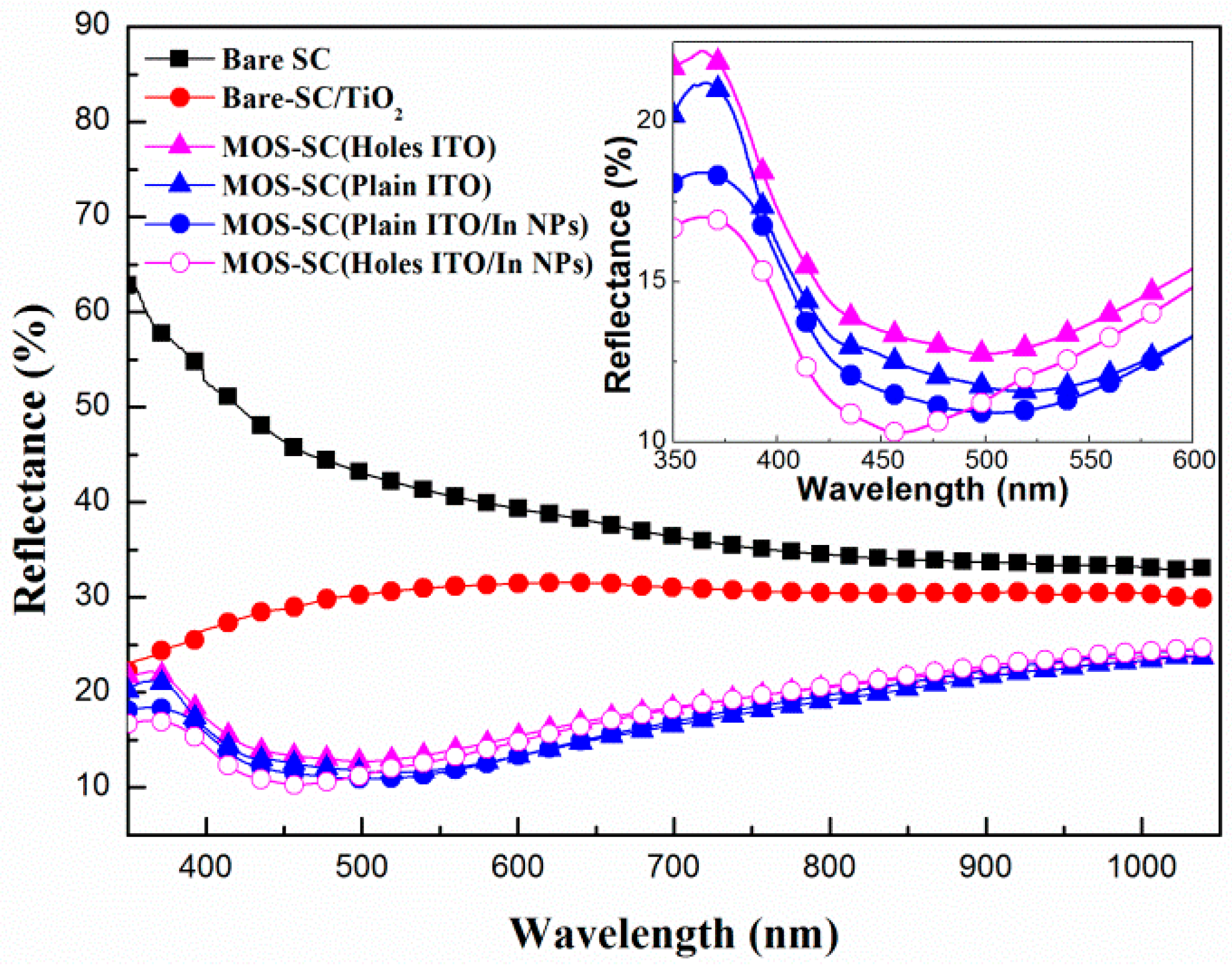
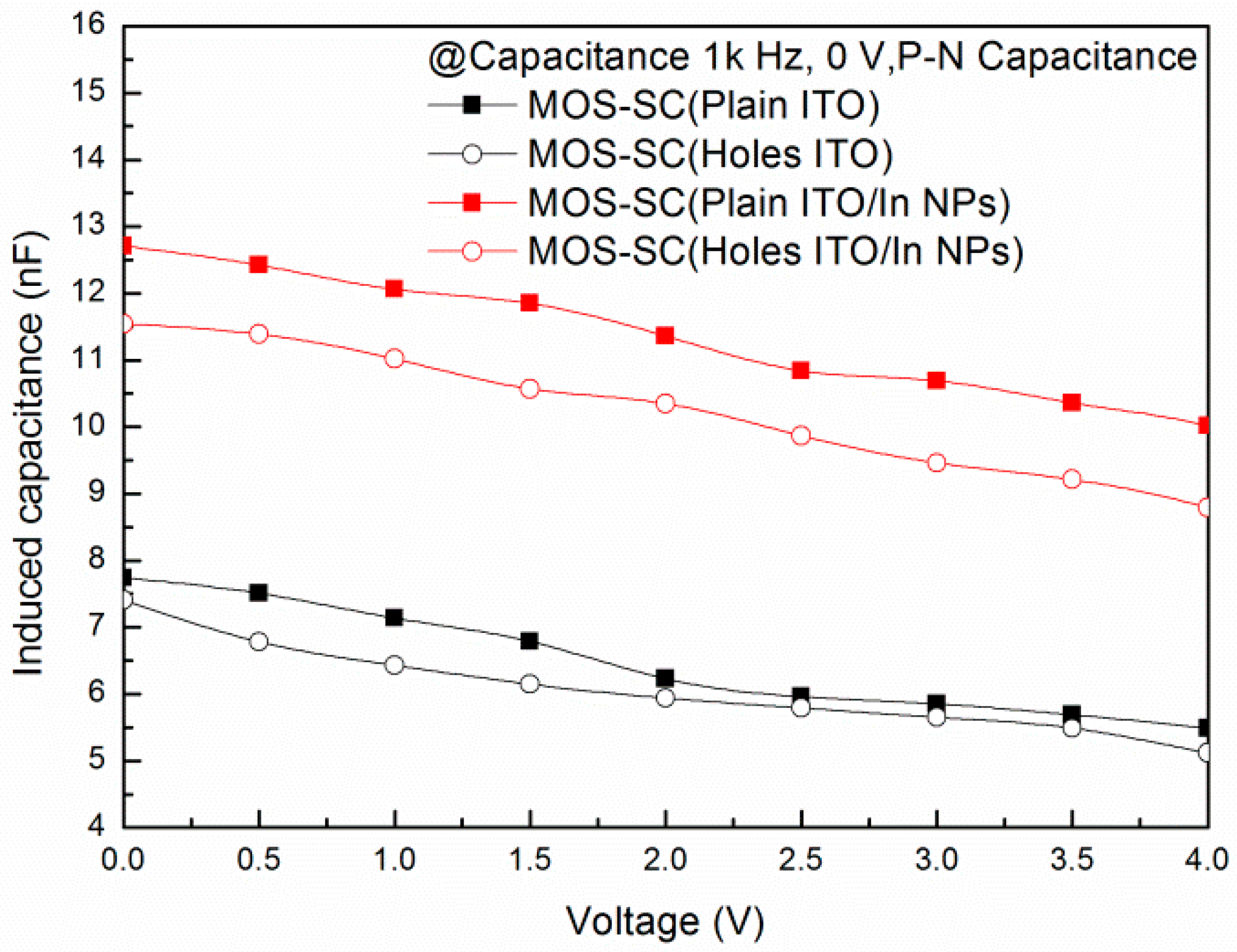
2. Results and Discussion

Figure 1 presents the dark I-V characteristics of a bare cell and a cell with a MOS structure at 25 °C. The ideality factor (n) and reverse saturation current density (J0) extracted from the measured I-V curves are listed in Table 1. The n and J0 values of the bare cell were 1.87 and 6.14 × 10⁻⁸ A/cm2, respectively. The n and J0 values of the MOS cell with plain ITO (with periodic holes–type ITO) were 1.51 (1.65) and 3.84 × 10⁻⁹ (1.82 × 10⁻⁸) A/cm2, respectively. These improvements can be attributed to the suppression of surface recombination through the application of a TiO2 dielectric film on the surface of the cell.
Figure 2 presents the optical reflectance of the bare cell, the cell with a film of TiO2, the MOS cell with a plain ITO electrode, the MOS cell with a perforated ITO electrode, the MOS cell with In-NPs and a plain ITO electrode, and the MOS cell with In-NPs and a perforated ITO electrode. The reflectance values of cells with a TiO2 coating or ITO/TiO2 structure were lower than those of the bare cell, due to the anti-reflective properties of TiO2 and ITO/TiO2. The reflectance of the cell with a plain ITO electrode was lower than that of the cell with a perforated ITO electrode, due to the fact that the perforations reduced the total area of the ITO, thereby reducing the anti-reflective effects. The MOS cell with In-NPs presented a blue shift in the optical reflectance curves and a lower overall reflectance due to the plasmonic light scattering of the In-NPs. As shown in the inset of Figure 3, the incorporation of perforated electrodes blue-shifted the reflectance curves from 500 to 450 nm and reduced reflectance by 11% (at a wavelength of 450 nm).
Figure 3a presents the EQE response of the six solar cells tested in this study. The EQE values of the cells with a TiO2 layer and the cell with an ITO/TiO2 structure were higher than that of the bare cell, due to the anti-reflective properties of TiO2 and ITO/TiO2. The EQE of the cell with a plain ITO electrode was higher than that of the cell with a perforated ITO electrode, due to the fact that the perforations reduced the total area of the ITO, thereby reducing the anti-reflective effects. The MOS cell with In-NPs presented an impressive improvement in EQE at wavelengths of 350–600 nm. Overall, the EQE response values are in good agreement with the results of optical reflectance. Figure 3b illustrates the improvements in EQE under the effects of the anti-reflective coatings in conjunction with plasmonic light scattering in the In-NPs. The plain ITO electrode was more effective than the perforated ITO electrode in improving EQE enhancement across the entire range of wavelengths. We observed a peak at approximately 500 nm corresponding to a trough in the reflective spectrum, which is indicative of an improvement in EQE. At wavelengths below 500 nm, the In-NPs improved EQE values in all samples (regardless of the ITO electrode used); however, the cells with a perforated electrode presented a more pronounced improvement in EQE at wavelengths between 350 and 880 nm.
Figure 4 presents the photovoltaic J-V curves of the bare cell, the cell with a film of TiO2, the MOS cell with a plain ITO electrode, the MOS cell with a perforated ITO electrode, and the MOS cell with In-NPs and a plain ITO electrode, and the MOS cell with In-NPs and a perforated ITO electrode. Table 2 lists the statistics data of the photovoltaic performance of the solar cells evaluated in this study. The short-circuit current density (Jsc) values of the cell with a layer of TiO2 (27.99, 29.65 mA/cm2) and the cell with an ITO/TiO2-layer structure (32.81, 33.71 mA/cm2) were higher than that of the bare cell (26.35, 26.88 mA/cm2), due to the anti-reflective properties of the TiO2 and ITO/TiO2. The Jsc of the MOS cell with a plain ITO electrode (33.71 mA/cm2, at 0 V bias) was higher than the cell with a perforated ITO electrode (32.81 mA/cm2, at 0 V bias) due to the large area of ITO and its anti-reflective properties. Clearly, the improvements in Jsc are proportional to the improvements in EQE as well as reduced reflectance. The improvement in Jsc provided by the In-NPs was 9.93% in the MOS cell with a plain ITO electrode and In-NPs (from 33.71 to 37.06 mA/cm2, under a bias voltage of 0 V), which is greater than the 5.18% of the cell with a perforated electrode (from 32.81 to 34.51 mA/cm2, under a bias voltage of 0 V).
Figure 5 presents the junction capacitance of all MOS cells. Measurements obtained at the front Al/Ti electrode and back Al electrode are a function of voltage applied to the ITO electrode. We observed a decrease in the induced capacitance with an increase in the bias voltage. These results indicate that the depletion width under the ITO region was enlarged. The induced capacitance of the MOS cell with a perforated ITO electrode was less than that of the cell with the plain ITO electrode due to a reduction in area. The large capacitance on all cells with In-NPs can be attributed to an increase in the surface area with integrated metallic particles.
Figure 6 presents photovoltaic J-V curves of the proposed MOS cell with both types of ITO electrodes (with and without In-NPs) and with and without bias voltage. The Jsc of the MOS cell with a perforated ITO electrode (44.84 mA/cm2, under a bias voltage of 4 V) was higher than the cell with a plain ITO electrode (40.49 mA/cm2, under a bias voltage of 4 V). The Jsc enhancements of 36.66% (from 32.81 to 44.84 mA/cm2) and 20.16% (from 33.71 to 40.49 mA/cm2) corresponding to the above-mentioned conditions were obtained due to the effects of the bias voltage. Furthermore, the Jsc of the MOS-structure cell with perforated ITO and In-NPs (45.13 mA/cm2, under a bias voltage of 4 V) was higher than that with the plain ITO and In-NPs (44.04 mA/cm2, under a bias voltage of 4 V) and the Jsc enhancements of 37.54% (from 32.81 to 45.13 mA/cm2) and 36.66% (from 33.71 to 44.04 mA/cm2) corresponding to the above-mentioned conditions can be attributed to plasmonic light scattering as well as biasing effects. It is interesting to note that under voltage bias, the improvements in Jsc are more pronounced in the MOS cell with a perforated ITO electrode than in the cell with a plain ITO electrode. Surface plasmon polaritons (SPPs) travel along ITO/TiO2 and the localized surface plasmon resonance (LSPR) of In-NPs can be attributed to efficient coupling and the scattering of incident light into the active layer of the cells. However, the underlying mechanism has yet to be fully elucidated and is undergoing further study.

3. Materials and Methods

3.1. Bare-Type P-N Silicon Solar Cell

A 525-μm-thick, boron-doped C-Si wafer with resistivity of 10 Ω·cm and (100) orientation was used as a substrate in this study. The wafers were cut into samples of 10 × 10 mm2 for the fabrication of silicon solar cells. After RCA (Radio Corporation of America) cleaning, an n+-Si emitter layer with sheet resistance of approximately 80 Ω/sq was applied to the C-Si wafer using a phosphor diffusion process in a rapid thermal annealing (RTA) chamber (eRTP-MV, Giant Technology Corporation, Taiwan) at 900 °C for 2 min. The oxide layer on the surface of the wafer was removed using hydrogen fluoride (HF) solution. Following the phosphor diffusion of the n+-Si emitter layer, a 200 nm Al film was deposited on the rear surface using electron-beam (e-beam) evaporation (EVM-8, Kao Duen Technology Corporation, New Taipei City, Taiwan) and then annealed at 450 °C for 5 min to form the back electrode with good ohmic contact. Finally, top-contact grid-electrodes were formed using a 20 nm Ti film and 300 nm Al film using photolithography lift-off and e-beam evaporation to create bare-type p-n Si solar cells. These bare-type Si solar cells (denoted as bare cells) were used as a reference with regard to optical reflectance (Lambda 35, PerkinElmer Inc., Waltham, MA, USA), dark current-voltage (I-V, HP 4145B, Hewlett Packard, Palo Alto, CA, USA), external quantum efficiency (Enli Technology Co. Ltd., Kaohsiung, Taiwan), and photovoltaic I-V under air mass (AM) 1.5 G illumination. The solar simulator (XES-151S, San-Ei Electric Co. Ltd., Osaka, Japan) was calibrated using a National Renewable Energy Laboratory (NREL)-certified crystalline silicon reference cell (PVM-894, PV Measurements Inc., Boulder, CO, USA) prior to measurement.

3.2. MOS-Structure Silicon Solar Cell

E-beam evaporation was then used to deposit a 20-nm-thick TiO2 film on the surface of the bare solar cell. This was followed by a 50-nm-thick ITO film using thermal sputtering (PSUVH-450, HOPE Vacuum Technology Co. Ltd., Chai-yi, Taiwan) over spaced Al-finger electrodes to construct an ITO electrode. Lift-off photolithographic processing resulted in the formation of an ITO-TiO2-Si structure, denoted as the MOS-structure solar cell. We also fabricated samples using a plain-type ITO electrode as well as samples with ITO electrodes with periodic holes referred to as perforations (these were added using lift-off photo-resister patterns). The holes on the ITO electrode formed a matrix-configuration of 2 × 88, wherein the hole diameter was 10 μm and hole spacing was 39 μm. We then measured the dark I-V curves, optical reflectance, EQE, and photovoltaic current density-voltage (J-V) of the MOS-structure cell, to enable comparison with the bare solar cell. These measurements further elucidated the passivation and anti-reflection effects of the ITO/TiO2 layer-structure. We also compared cells with plain ITO electrodes and perforated ITO electrodes with regard to electric and optical performance. Enhancements in photovoltaic performance and reductions in p-n junction capacitance were indicated by photovoltaic J-V and C-V measurements (HP 4274A, Hewlett Packard), during which bias voltage was applied to the ITO electrode.

3.3. MOS-Structure Silicon Solar Cell with In-NPs

Finally, we deposited a 3.8-nm-thick film of indium (In) on the surface of the MOS-structure solar cells using e-beam evaporation followed by annealing at 200 °C for 10 min in a rapid thermal annealing chamber under ambient H2 to produce In-NPs. Figure 7a presents a Scanning electron microscopy (SEM; Hitachi S-4700, Hitachi High-Tech Fielding Corporation, Tokyo, Japan) image of In-NPs profile deposited on ITO surface. The average diameter and coverage of the In-NPs were 17.70 nm and 30.5%, respectively. The objective was to evaluate the effect of plasmonic scattering induced by the In-NPs on the performance of MOS cells. We also sought to evaluate the performance of MOS cells with In-NPs with and without applied bias voltage based on photovoltaic J-V measurements. Figure 7b illustrates the proposed MOS-structure solar cell with In-NPs and a perforated ITO-electrode.

4. Conclusions

This paper reports MOS-structure silicon solar cells with plain ITO electrodes or perforated ITO electrodes (with or without plasmonic In-NPs) under an applied bias voltage of 0 to 4 V. The efficiency of the MOS-structure cells with perforated ITO electrodes (17.80%) is superior to that of cells with plain ITO electrodes (16.87%) and coated In-NPs under a bias voltage of 4 V. It appears that the application of bias voltage to the ITO electrode increased the depletion width and enhanced the collection efficiency of photo-carriers. Moreover, surface plasmon polaritons along the ITO/TiO2 as well as the localized surface plasmon resonance of In-NPs are responsible for the efficient coupling and scattering of incident light into the active layer of the cells, resulting in enhanced efficiency.

Acknowledgments

The authors would like to thank the Ministry of Science and Technology of the Republic of China for financial support under Grant MOST 103-2221-E-027-049-MY3.

Author Contributions

All the authors conceived the experiments; W.J. designed, analyzed, and wrote the first draft of the paper; R.S. and J.C. performed the experiments; H.J. and C.F. provided EQE measurement and analysis; all the authors contributed to the discussion of the paper.

Conflicts of Interest

The authors declare no conflict of interest.

References

  1. Taguchi, M.; Kawamoto, K.; Tsuge, S.; Baba, T.; Sakata, T.; Morizane, M.; Uchihashi, K.; Nakamura, N.; Kiyama, S.; Oota, O. HIT™ cells—High-efficiency crystalline Si cells with novel structure. Prog. Photovolt. Res. Appl. 2000, 8, 503–513. [Google Scholar] [CrossRef]
  2. Zhong, S.; Hua, X.; Shen, W. Simulation of high-efficiency crystalline silicon solar cells with homo–hetero junctions. IEEE Trans. Electron Dev. 2013, 60, 2104–2110. [Google Scholar] [CrossRef]
  3. Taguchi, M.; Terakawa, A.; Maruyama, E.; Tanaka, M. Obtaining a higher Voc in HIT cells. Prog. Photovolt. Res. Appl. 2005, 13, 481–488. [Google Scholar] [CrossRef]
  4. Pillai, S.; Green, M.A. Plasmonics for photovoltaic applications. Sol. Energy Mater. Sol. Cells 2010, 94, 1481–1486. [Google Scholar] [CrossRef]
  5. Fan, X.; Zheng, W.; Singh, D.J. Light scattering and surface plasmons on small spherical particles. Light Sci. Appl. 2014, 3, 1–14. [Google Scholar] [CrossRef]
  6. Luk’yanchuk, B.S.; Tribel’ski, M.I.; Ternovski, V.V. Light scattering at nanoparticles close to plasmon resonance frequencies. J. Opt. Technol. 2006, 73, 371–377. [Google Scholar] [CrossRef]
  7. Ho, W.J.; Su, S.Y.; Lee, Y.Y.; Syu, H.J.; Lin, C.F. Performance-enhanced textured silicon solar cells based on plasmonic light scattering using silver and indium nanoparticles. Materials 2015, 8, 6668–6676. [Google Scholar] [CrossRef]
  8. Atwater, H.A.; Albert, P. Plasmonics for improved photovoltaic devices. Nat. Mater. 2010, 9, 205–213. [Google Scholar] [CrossRef] [PubMed]
  9. Cotal, H.; Fetzer, C.; Boisvert, J.; Kinsey, G.; King, R.; Hebert, P.; Yoon, H.; Karam, N. III–V multijunction solar cells for concentrating photovoltaics. Energy Environ. Sci. 2009, 2, 174–192. [Google Scholar] [CrossRef]
  10. Yamaguchi, M.; Takamoto, T.; Araki, K.; Ekins-Daukes, N. Multi-junction III–V solar cells: Current status and future potential. Sol. Energy 2005, 79, 78–85. [Google Scholar] [CrossRef]
  11. Yamaguchi, M. Multi-junction solar cells and novel structures for solar cell Applications. Phys. E 2002, 14, 84–90. [Google Scholar] [CrossRef]
  12. Pudasaini, P.R.; Ayon, A.A. Nanostructured plasmonics silicon solar cells. Microelectron. Eng. 2013, 110, 126–131. [Google Scholar] [CrossRef]
  13. Pudasaini, P.R.; Ayon, A.A. Nanostructured thin film silicon solar cells efficiency improvement using gold nanoparticles. Phys. Status Solidi A 2012, 209, 1475–1480. [Google Scholar] [CrossRef]
  14. Sharma, M.; Pudasaini, P.R.; Ruiz-Zepeda, F.; Vinogradova, E.; Ayon, A.A. Plasmonic effects of Au/Ag bimetallic multispiked nanoparticles for photovoltaic applications. ACS Appl. Mater. Interfaces 2014, 6, 15472–15479. [Google Scholar] [CrossRef] [PubMed]
  15. Kuhlmann, B.; Aberle, A.G.; Hezel, R.; Heiser, G. Simulation and optimization of metal–insulator–semiconductor inversion-layer silicon solar cells. IEEE Trans. Electron Dev. 2000, 47, 2167–2178. [Google Scholar] [CrossRef]
  16. Chattopadhyay, P. A novel low resistive metal-insulator-semiconductor (MIS) inversion layer solar cells structure. Solid-State Electron. 1988, 31, 1641–1643. [Google Scholar] [CrossRef]
  17. Lam, Y.W.; Green, M.A.; Davies, L.W. Electrostatic effects in inversion-layer metal-insulator-semiconductor solar cells. Appl. Phys. Lett. 1980, 37, 1087–1089. [Google Scholar] [CrossRef]
  18. Oener, S.Z.; Van de Groep, J.; Macco, B.; Bronsveld, P.C.P.; Kessels, W.M.M.; Polman, A.; Garnett, E.C. Metal–Insulator–Semiconductor Nanowire Network Solar Cells. Nano Lett. 2016, 16, 3689–3695. [Google Scholar] [CrossRef] [PubMed]
  19. Hezel, R. Recent progress in MIS solar cells. Prog. Photovolt. Res. Appl. 1997, 5, 109–120. [Google Scholar] [CrossRef]
  20. Ho, W.J.; Huang, M.C.; Lee, Y.Y.; Hou, Z.F.; Liao, C.J. Performance enhancement of ITO/oxide/semiconductor MOS-structure silicon solar cells with voltage biasing. Nanoscale Res. Lett. 2014, 9. [Google Scholar] [CrossRef] [PubMed]
  21. Yerokhov, V.Y.; Melnyk, I.I.; Korovin, A.V. External bias as the factor of efficiency increase of silicon MIS/IL solar cells. Sol. Energy Mater. Sol. Cells 1999, 58, 225–236. [Google Scholar] [CrossRef]
  22. Ho, W.J.; Hsieh, M.L.; Lee, Y.Y.; Liu, J.J.; Syu, J.K.; Lai, Q.R.; Yu, C.M. Efficiency improvement of 25.7% using a voltage biasing transparent electrode for MIS transistor-based silicon solar cells. Surf. Coat. Technol. 2013, 231, 447–451. [Google Scholar] [CrossRef]
Figure 1. Dark I-V characteristics of bare cell and cells with MOS structure (using plain and perforated electrodes) at 25 °C.
Materials 09 00682 g001
Figure 2. Optical reflectance of bare cell, cell with TiO2 film, MOS cell with plain ITO electrode, MOS cell with perforated ITO electrode, MOS cell with plain ITO electrode and In-NPs, and MOS cell with perforated ITO electrode and In-NPs.
Materials 09 00682 g002
Figure 3. (a) EQE response of all solar cells tested in this study; (b) EQE enhancement can be attributed to anti-reflective properties and plasmonic light scattering.
Materials 09 00682 g003
Figure 4. Photovoltaic J-V curves of all solar cells tested in this study (without applied bias voltage).
Materials 09 00682 g004
Figure 5. Induced capacitance of all MOS cells: measurements obtained at the front Al/Ti electrode and back Al electrode are a function of voltage applied to the ITO electrode.
Materials 09 00682 g005
Figure 6. Photovoltaic J-V curves of MOS cells with and without In-NPs as a function of voltage applied to the ITO electrode (0 and 4 V).
Materials 09 00682 g006
Figure 7. (a) SEM images showing the size and profile of In-NPs; (b) Schematic diagram of proposed MOS solar cell with In-NPs and perforated ITO-electrode.
Materials 09 00682 g007
Table 1. Ideality factor (n) and reverse saturation current density (J0) extracted from measured I-V curves at 25 °C.
Cell TypenJ0 (A/cm2)
Bare SC1.876.14 × 10−8
MOS SC (Plain ITO)1.513.84 × 10−9
MOS SC (Holes ITO)1.651.82 × 10−8
Table 2. Summary of photovoltaic performance of all solar cells evaluated in this study.
Cell #Bare SCTiO2/SCMOS SC at 0 VMOS SC at 4 VMOS SC w/In NPs, at 0 VMOS SC w/In NPs, at 4 V
Voc (mV) aITO (Holes)Cell-1539.3543.2547.0557.6545.1554.3
Cell-2533.8541.1543.2553.2542.6552.4
Average536.6542.2545.1555.4543.9553.4
ITO (Plain)Cell-1527.9531.8538.4542.7535.3541.2
Cell-2526.6532.2539.7544.3537.2542.8
Average527.3532.0539.1543.5536.3542.0
Jsc (mA/cm2)ITO (Holes)Cell-126.3527.9932.8144.8434.5145.13
Cell-226.8228.5333.0745.9834.8446.38
Average26.5928.2632.9445.4134.6845.76
ITO (Plain)Cell-126.8829.6933.7140.4937.0644.04
Cell-226.3828.8133.1540.1236.4743.52
Average26.6327.7533.4340.3136.7743.78
FF (%) bITO (Holes)Cell-175.475.873.870.174.571.1
Cell-275.075.174.369.474.969.8
Average75.275.574.169.874.770.5
ITO (Plain)Cell-174.675.174.471.971.770.8
Cell-275.175.474.872.072.370.4
Average74.975.374.672.072.070.6
η (%) cITO (Holes)Cell-110.7211.5313.2417.5314.0117.80
Cell-210.7411.5913.3517.6414.1617.88
Average10.7311.5613.3017.5914.0917.84
ITO (Plain)Cell-110.5911.8513.5015.8014.2316.87
Cell-210.4311.5613.3815.7214.1616.63
Average10.5111.7113.4415.7614.2016.75
a Voc: open-circuit voltage; b FF: fill factor; c η: conversion efficiency.

