A Review of DSP-Based Enabling Technologies for Cloud Access Networks


1
School of Electronic Engineering, Bangor University, Dean Street, Bangor LL57 1UT, UK
2
ADVA Optical Networking, ADVAntage House, Tribune Way, York YO30 4RY, UK
3
College of Electronics Engineering, Electronics department, Ninevah University, Mosul 41001, Iraq
4
Key Laboratory of Specialty Fiber Optics and Optical Access Networks, Shanghai University, Shanghai 200072, China
*
Author to whom correspondence should be addressed.
Future Internet 2018, 10(11), 109; https://doi.org/10.3390/fi10110109
Submission received: 28 September 2018
/
Revised: 3 November 2018
/
Accepted: 11 November 2018
/
Published: 15 November 2018
(This article belongs to the Special Issue Recent Advances in DSP-Based Optical Communications)
Abstract
:Optical access networks, metro networks and mobile data networks are facing rapidly evolving demands, not only is it essential to satisfy the unyielding need for increased user bandwidths, but future networks must also support the growing wide variation in traffic dynamics and characteristics, due to various emerging technologies, such as cloud-based services, the Internet-of-Things (IoT) and 5G mobile systems, and due to growing trends, such as the proliferation of mobile devices and the rapidly increasing popularity of video-on-demand services. To be cost-effective and commercially sustainable, future optical networks must offer features, such as, dynamic reconfigurability, highly efficient use of network resources, elastic bandwidth provisioning with fine granularity, network sliceabilty and software defined networking (SDN). To meet these requirements Cloud Access Networks (CANs) are proposed which require a number of flexible, adaptive and reconfigurable networking elements. By exploiting digital signal processing (DSP) we have proposed a digital orthogonal filter-based multiplexing technique to implement CANs with multiplexed, independent optical channels at the wavelength, sub-wavelength, and orthogonal sub-band levels. This paper reviews the overall CAN concept, the operating principles of the various CAN network elements and presents an overview of the research work we have undertaken in order to validate the feasibility of the proposed technologies which includes real-time DSP-based demonstrations.
1. Introduction
Today’s communication networks are increasingly struggling to support the growing demands of emerging network services and traffic, such as the higher data rates, drastically increased the number of connections and ultra-low latency requirements of 5G. Traditionally networks have been designed with an essentially static architecture [1,2] which provides end users with fixed capacity internet connections. If end users require a change to their connection speed this can require manual operator intervention and can take significant time to implement as potentially physical hardware must be replaced, thus bandwidth provision is fundamentally static in nature. As internet connection speeds started to steadily increase, operators have been able to increase subscription rates to maintain a viable business model based on the fixed capacity provision. However, it is predicted, that to meet traffic growth demands in the future, operators must offer multi-Gb/s internet connection speeds [3], but provision of multi-Gb/s connections is highly challenging to achieve in a cost-effective manner as subscribers are not prepared to pay significantly increased subscription rates, thus operators are facing the dilemma of the decoupling effect between traffic growth and revenue growth. Networks must, therefore, evolve to offer advanced, highly agile, dynamically reconfigurable architectures that support features, such as elastic bandwidth allocation, network slicing and SDN control. These dynamic networks [4,5] would thus allow operators to instantly respond to changing traffic demands, offering network features, such as elastic connectivity tailored to the end users’ prevailing needs, automatic network reconfiguration based on identified traffic patterns and provision of dedicated virtual networks with service critical characteristics, such as security and latency. These new dynamic network architectures can, therefore, be cost-effective and commercially viable as highly efficient use of the available network resources is achieved and operators can also decouple their revenue from pure data capacity provision and link it more to on-demand network service provision.
To realise highly dynamic networks at the physical layer, we have proposed Cloud Access Networks (CANs) [6,7] which employ flexible, adaptive and reconfigurable networking elements. By exploiting optical transceiver-embedded digital signal processing (DSP) we have proposed a digital orthogonal filter-based multiplexing technique to implement CANs with multiplexed, independent optical channels at the wavelength, sub-wavelength (Sub-λ) and orthogonal sub-band (Sub-B) levels [8,9]. The objective of this paper is to review our recent work on DSP-based technologies for enabling CANs, thus it provides a unique insight into the overall capabilities of a CAN, facilitated by the various complementary technologies. The overall CAN concept is presented in Section 2, and Section 3 presents the operating principles of the various DSP-based CAN network elements, along with an overview of our associated real-time DSP-based research work. Finally, Section 4 concludes the paper.
2. Cloud Access Network Concept
2.1. Overview
The basic concept of the CAN is the provision of a SDN-controlled network that is dynamically reconfigurable to offer users’ on-demand connectivity according to the users’ application requirements, for example, bit rate, latency, security and reliability-level, also new connectivity features, such as ultra-low power idle states can meet the need for greener networks. The proposed CAN offers a number of key characteristics and features:
- Seamless integration of Metro-networks, fixed access networks, and 4G/5G fronthaul and backhaul networks.
- Provision of a sliceable and dynamically reconfigurable network which can efficiently support virtualised networks at sub-wavelength connectivity levels with elastic bandwidth provision.
- Full support of SDN for efficient control and management of the network configuration, with control extended to the physical layer.
- Support of DSP-based advanced modulation formats to achieve spectrally efficient high-speed interconnections.
- Channel transparency to underlying signal characteristics, such as bandwidth and modulation format.
- Excellent backwards compatibility with existing optical transmission technologies as the baseband region in the optical domain can be allocated to existing TDM-based optical signals.
- Dynamically reconfigurable and highly flexible network elements.
- Exploitation of existing passive optical network (PON) infrastructures by the use of advanced multiple access techniques.
- Enhanced physical layer data security the as full details of the channel multiplexing parameters are required to perform data recovery.
- An inherent “pay as you grow” network operation model, as the growing demand for aggregate capacity can be met by adding additional channels to the network as required.
2.2. Digital Orthogonal Filtering-Based Channel Multiplexing
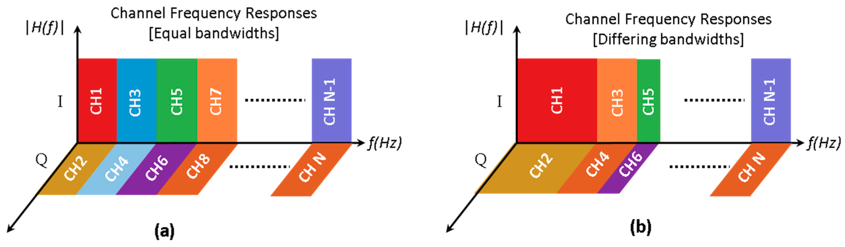
The CAN concept is built upon the principle of DSP-based channel multiplexing using digital orthogonal filters. As channel multiplexing and demultiplexing are performed in the digital domain [9], this allows great flexibility in network connectivity due to the intrinsic versatility of DSP circuits. Furthermore, low-cost implementation is achieved by avoiding expensive RF and optical components and leveraging the economies of scale associated with mass produced digital integrated circuits (ICs). Figure 1 illustrates the basic principle of channel multiplexing/demultiplexing by digital orthogonal filtering, where reconfigurable digital orthogonal filters embedded in digital ICs within the optical transceivers are used to multiplex/demultiplex N bandwidth-variable channels. For each channel, an independently modulated signal is first up-sampled via the insertion of M-1 zeros between two consecutive samples, thus the up-sampling factor is M, denoted as (M↑). The up-sampling generates M/2 double-sideband spectral images within the Nyquist frequency band, the up-sampling factor, therefore, allows control of the generated channel bandwidth (bandwidth = sampling frequency/M). Subsequently, a digital shaping filter (SF) is employed to select the appropriate spectral image to locate the signal at the desired spectral location, that is, in the desired sub-wavelength channel. By using Hilbert-pair filters, two signals can be co-located in the same sub-wavelength channel. The Hilbert-pair filters generate orthogonal channels as the In-phase (I) filter applies a 0° phase shift to all frequency components, whereas the Quadrature-phase (Q) filter applies a −90° phase shift to all frequency components, thus two orthogonal sub-band channels occupy the same sub-wavelength channel. The two orthogonal channels are thus denoted as the I (In-phase) and Q (Quadrature-phase) channels. The generated channels are all summed together in the digital domain and fed to a single DAC. The resulting analogue electrical signal then drives a suitably biased optical intensity modulator (IM) and the optical signal is launched into an intensity modulation and direct-detection (IMDD) network employing standard single mode fibre (SSMF). After transmission through the network, in the receiver a photo detector (PD) converts the optical signal to an electrical for digitisation by an ADC, the digital signal is then fed to one or more DSP-based receivers, each dedicated to recovering a specific channel. In the DSP receivers the digital signal is first filtered by the appropriate digital matching filter (MF) to demultiplex the desired channel from the aggregated signal, subsequent down-sampling by a factor of M, denoted as (M↓), is performed by selecting every M-th sample, which returns the signal to baseband at the original sample rate. Sample timing alignment is necessary for the receiver (not shown in Figure 1) to ensure correct filter operation. Finally, the received signal from each channel is demodulated according to the adopted signal modulation to recover the encoded binary data. Full details of the theory underpinning the digital orthogonal filer-based multiplexing can be found in [9,10]. Figure 2a,b show example spectra of different combinations of digital orthogonal filter multiplexed channels for the cases of equal and varying channel bandwidths respectively.
A vitally important characteristic of the aforementioned channel multiplexing technique is that channels can be routed and switched completely in the optical domain without the need for optical-electrical-optical (OEO) conversion or optical bandpass filters (OBPFs), thus allowing the realisation of low-cost network switching devices which are crucial for the cost-sensitive CAN scenarios and moreover, the optical domain channel switching devices can achieve negligible latency which is a key advantage when considering the ultra-low latency requirements of 5G. Optical domain channel switching devices for CAN applications are discussed in detail in Section 3.2 and Section 3.3. Furthermore, the technique can allow the implementation of highly flexible multiple access PONs [9] based on channel multiplexing in the optical domain, where multiple independently generated optical channels or groups of channels are passively combined in the optical domain with a simple passive coupler [6].
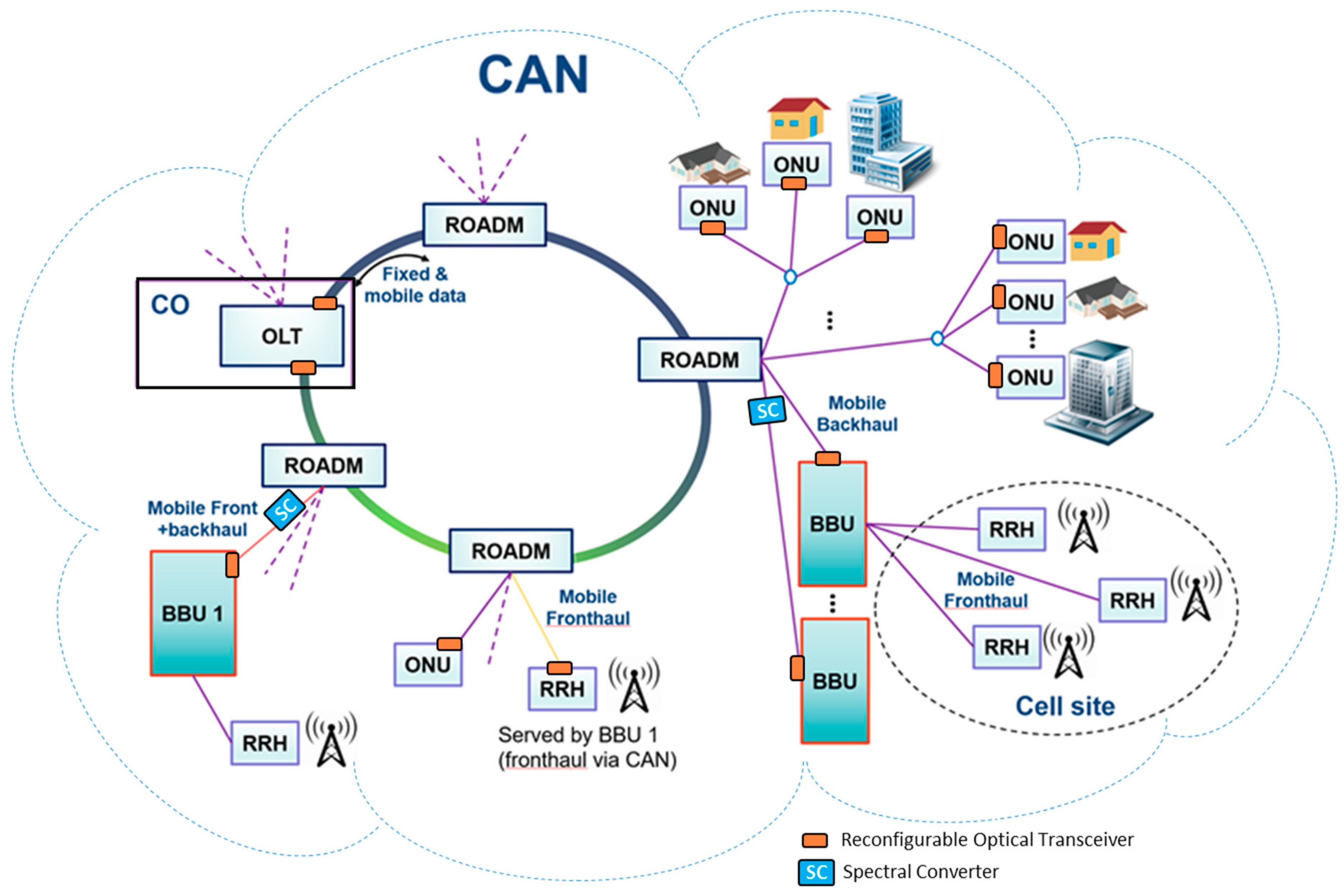
2.3. CAN Architecture
An example CAN architecture is illustrated in Figure 3. The CAN connects multiple end-points to an optical line terminal (OLT) in the operator’s central office (CO), where the connectivity to the core network is provisioned. The data connections within the CAN can support fixed data, mobile backhaul or mobile fronthaul, thus the end-points would be optical network units (ONUs) for fixed data links, baseband units (BBUs) for backhaul links and remote radio heads (RRHs) for front-haul links. The CAN can also support direct connectivity between end-points within the CAN, thus completely bypassing the OLT. For example, fronthaul links can be established between BBUs and RRHs at different locations in the CAN and dedicated fixed data links can be established between two end users connected to the CAN, such as a private network between two different offices of a business. There are three key networking devices that achieve the dynamic interconnectivity of the CAN, reconfigurable optical transceivers (ROTs), soft-reconfigurable optical add/drop multiplexer (soft-ROADMs) and spectral converters (SCs).
The ROTs are embedded within the ONUs/BBUs/RRHs and within the OLT, key characteristics of the ROTs are:
- They form the link terminations and are the only points at which optical-electrical (OE) and electrical-optical (EO) conversion occurs.
- They incorporate the embedded DSP which realises the digital orthogonal filtering-based channel multiplexing.
- The only point at which signals are modulated and demodulated as the CAN is transparent to signal modulation formats.
- Provide variably/adaptively modulated signals with variable bandwidth located within the digital orthogonal filtering space.
- Support SDN control via a centralised SDN controller, to manage channel allocation and avoid possible channel contention.
Multiple soft-ROADMs would be interconnected, for example in a ring architecture, as shown in Figure 3, to allow channels to be added and dropped as required to allow dynamic distribution of the total CAN capacity to the various end-points in the network. Wavelength division multiplexing (WDM) is fully supported by the soft-ROADMs thus allowing high-level channel multiplexing at the wavelength level. Each wavelength supports the aforementioned DSP-enabled sub-wavelength and orthogonal sub-band level channels, which can be dynamically switched by the soft-ROADMs channel add/drop functions. Key features of the soft-ROADMs are:
- Operation completely in the optical domain, thus avoiding the need for OE and EO conversions.
- Supports WDM-multiplexed optical signals.
- Channel add/drop functions operating at the wavelength, sub-wavelength and orthogonal sub-band levels.
- Provides connectivity to one or more PONs with dynamically variable capacity.
- Provision of mobile backhaul links to BBUs with dynamically variable capacity.
- Provision of mobile fronthaul links between BBUs and RRHs at different locations in the CAN and with dynamically variable capacity.
- Transparent to the underlying signal modulation formats.
- Fully compatible with SDN-based network control.
- Virtually negligible latency for compliance with the ultra-low latency 5G requirements.
The soft-ROADM thus provides channel level switching at the wavelength, sub-wavelength and orthogonal sub-band levels, thus offering dynamic bandwidth allocation with a granularity below the wavelength level. To achieve even finer bandwidth granularity, a single channel can be shared by multiple end users by employing multiple access modulation formats. For example, orthogonal frequency division multiplexing (OFDM) supports multiple subcarriers which can be independently allocated to different end users. Thus a channel supporting an OFDM modulated signal can be added/dropped by a soft-ROADM to support an OFDM-multiple access (OFDMA) PON.
To allow increased flexibility in network configuration and versatility, spectral converters have also been proposed and investigated [11], which enables signals to be converted from one spectral location to a new spectral location, purely in the optical domain, thus an optical signal can be relocated to occupy a different spectral location. The spectral converter can, therefore, eliminate the probability of channel blocking and allow increased channel utilisation. For example, if a signal is located in a specific spectral position and is to be added to an aggregated signal which does not have that specific spectral position unoccupied the spectral converter can be used to relocate the signal to a free spectral position before combination with the aggregate signal in the soft-ROADM. Compared to existing spectral converter technologies [12,13] the proposed spectral converters have the following key features:
- Low complexity and thus low cost due to no OE or EO converters or extra light sources.
- Virtually no distortion to the converted signal waveform.
- Strict transparency to the underlying signal characteristics.
- SDN-controllable reconfigurability of parameters, such as conversion efficiency, and frequency detuning range.
- The utilisation of optical bandwidth outside the operating range of the ROTs.
- Conversion-induced latency is negligible.
The fact that the spectral converters can reposition signals in the optical spectrum, with frequency detuning range potentially as large as 50 to 100 GHz, means that optical bandwidth outside the operating bandwidth of the ROTs can also be utilised, as signals can be spectrally up-shifted, transported through the CAN and then spectrally down-shifted. This also provides a means of cost effectively, incrementally scaling up network capacity, as spectral converters can be added as needed without the need to upgrade ROTs with higher bandwidth ROTs.
The aforementioned CAN network elements, therefore, enable the realisation of a CAN with a highly dynamic architecture, as it can be reconfigured on demand by a centralised SDN controller, to meet the traffic demands of the prevailing services. This highly flexible network with dynamic bandwidth provision thus allows the operator to change from the traditional operating model of fixed bandwidth provision and offer service driven, cost-effective bandwidth provision, thus offering an agile, responsive and future-proof network that can support the emerging and constantly evolving network applications.
3. CAN Network Elements
3.1. Reconfigurable Optical Transceivers
3.1.1. Operating Principle and Design Aspects
The reconfigurable optical transceivers are based on DSP-embedded digital orthogonal filters implemented with finite impulse response (FIR) filters with fully software-reconfigurable filter coefficients. The ROTs can be implemented as single or multi-channel devices. For each ROT channel the transmitter DSP performs signal modulation, up-sampling, filtering by digital orthogonal shaping filters and channel summation in the case of multi-channel devices, whereas the receiver DSP performs filtering by digital orthogonal matching filters, down-sampling and signal demodulation for each of the supported channels, thus the ROT DSP implements the digital orthogonal filtering-based channel multiplexing as described in Section 2.2 and illustrated in Figure 1. As different modulation formats offer trade-offs between signal parameters, such as spectral efficiency, minimum optical signal-to-noise ratio (OSNR) and power consumption, the ROT’s DSP can be designed to support multiple modulation formats and/or adaptive modulation formats for enhanced transmission performance flexibility. The ROTs can also be designed to support variable bandwidth channels by incorporating programmable up/down-sampling factors. To select a ROT’s required operating channel(s), the FIR filter coefficients are simply reconfigured in the shaping (matching) filters in the transmitter (receiver) DSP, to select the desired sub-band and channel phase (I or Q). A ROT-embedded DSP controller performs filter configuration by which communicating with a centralized SDN controller responsible for managing all connectivity within the CAN.
The ROTs incorporate a suitable DAC and IM in the transmitter side and a PD and ADC in the receiver side, along with any necessary RF gain stages, IM and PD biasing and temperature control circuitry. As the DAC/ADC will operate at multi-GS/s it is necessary to employ parallel processing in the DSP designs to achieve the required total sample throughput, as the digital integrated circuit (IC) operating speeds are of the order of several 100 s of MHz, thus parallel architecture FIR filters must be adopted.
As the digital orthogonal filters are implemented as FIR filters the design of the filters impacts on transmission performance. Parameters, such as the selected baseband pulse [9] for the Hilbert-pair filters, tap count and sample/coefficient bit resolutions can all impact the filter characteristics in comparison to the ideal filter, therefore when designing the filters a trade-off is needed between filter complexity and performance. Trade-offs in performance and filter design complexity have been extensively investigated in [8,9] where the effect of filter length and the α parameter (which determines the filters excess of bandwidth) were analysed, the analysis allowed the identification of optimum filter design guidelines for various scenarios.
An important characteristic of the digital orthogonal filters is that their complexity does not increase with increasing CAN channel count (all channels at minimum bandwidth) as the up-sampling and down-sampling result in inherent redundancy within the filter implementations [14].
Sample timing synchronization is required for correct operation of the ROTs. Not only is correct sample timing critical in the ROT receiver, but it is also critical in the ROT transmitter for the case of multipoint-to-point (MPTP) networks where orthogonal sub-bands are combined in the optical domain [15]. In all of our experimental demonstrations manual sample timing alignment is employed, however investigations into the effect of sample timing offset (STO) in point-to-point and MPTP networks has been investigated [16] for different levels of channel frequency response roll-off.
3.1.2. DSP Architecture and Real-Time Experimental Demonstrations
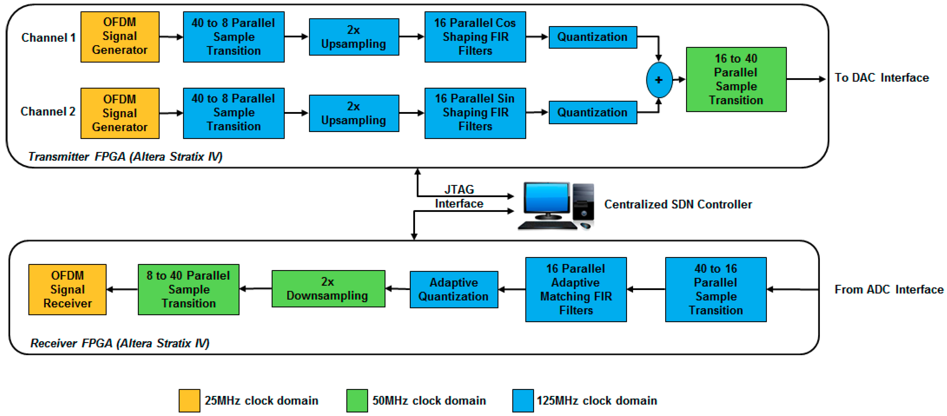
Figure 4 illustrates the DSP architectures of the demonstrated FPGA-based ROTs incorporating on-line reconfigurable digital orthogonal filters. For the demonstration, a two channel real-time transmitter and the single channel real-time receiver are employed. In the transmitter FPGA, two separate digital OFDM modulators incorporating adaptive bit and power loading generate two independent OFDM-modulated digital signals. The OFDM signal generation is described in detail in [17], and employs the OFDM parameters specified in Table 1, thus each individual OFDM symbol consists of 40 × 8-bit parallel samples at a symbol rate of 25 M symbols/s. The OFDM modulator sub-systems thus utilise a 25 MHz clock domain within the FPGA, as shown in Figure 4.
To significantly reduce the logic resource usage of the digital filters, each OFDM symbol is converted to eight parallel samples at an increased clock speed of 125 MHz, as shown in Figure 4. A clock domain of 125 MHz is therefore used for the digital filters. To achieve the channel multiplexing, as described in Section 2.2, each OFDM channel is first up-sampled by a factor of 2, this doubles the samples per symbol to 80 and increases the sample rate to 2 GS/s. The up-sampled channel is then passed through a bank of parallel 32-tap FIR digital shaping filters, with signed 8-bit filter coefficients. As the FPGA can only operate at 100 s MHz, parallel FIR filters are necessary to achieve the required 2 GS/s throughput. Thus 16 parallel samples at 125 MHz achieves a sample throughput of 2 GS/s. For the two-channel system implemented here, in the up-sampling function, zero-valued samples are not physically inserted before input to the FIR filters, this is because the FIR filters operate on parallel samples so it is not necessary to include multipliers for tap coefficients corresponding to the zero-valued samples. Moreover, a feature which is unique to the two channel system, due to the filter characteristics, is that every second output sample will be zero-valued, thus due to the parallel filter architecture only eight parallel FIRs are physically required to produce the 16 parallel output samples as eight output samples are fixed at zero-value. Each digitally filtered channel output is quantised to eight bits and then the channels are directly summed. To comply with the DAC interface implementation the 16 parallel samples are converted to 40 parallel samples, at a clock rate of 50 MHz, as shown in Figure 4. The multiplexed channels are, subsequently, inputted into the DAC interface block, which interfaces to an 8-bit, 2 GS/s DAC.
To recover a desired channel in the receiver FPGA, the 40 parallel samples clocked at 50 MHz, output from the ADC interface, are converted to 16 parallel samples clocked at 125 MHz before being input to the online reconfigurable digital matching filter. The 16 parallel samples output from the matching filter are subsequently down-sampled by a factor of 2 by removing every second sample. This produces eight parallel samples, which are converted to 40 parallel samples to match the interface of the OFDM decoder function. Thus, the receiver employs bus width conversions and clock domains similar to those used in the transmitter, with the signal now flowing in the opposite direction. To recover a specific channel, the coefficients of the matching filter are dynamically reconfigured to set its impulse response to correspond to the required matching filter.
The complete real-time ROT experimental system setup is shown in Figure 5 and the key system parameters are listed in Table 1. In the transmitter, the digital samples are converted via a DAC to an analogue electrical signal with a bandwidth of 1 GHz. An optimum RF signal voltage level is generated by an RF gain stage consisting of an RF amplifier and a variable electrical attenuator (VEA), the RF signal is then combined, via a bias-T, with an optimised DC bias voltage. The generated RF signal subsequently intensity modulates an electro-absorption modulated laser (EML) device which integrates a 1550 nm DFB laser (as the laser source) and a 10 GHz electro-absorption modulator (EAM). The EML produces an optical output at 2.5 dBm, which is subsequently launched into a 25 km SSMF IMDD system.
At the receiver, the received optical power (ROP) level is controlled by a variable optical attenuator (VOA), before optical-electrical conversion by a 12.4 GHz PIN + TIA. The generated analogue electrical signal level is carefully optimized via an RF amplifier and VEA to occupy the full-scale range of the 8-bit, 2 GS/s ADC. An RF delay line (not shown in Figure 5) is also utilised to adjust the receiver sample timing of the ADC. The digitized samples are transferred via the receiving FPGA’s deserialiser-based ADC interface before processing by the aforementioned receiver DSP, where the techniques in [18,19] are employed for OFDM symbol synchronization and subcarrier equalization.
The FPGA’s embedded logic analyser is utilised for performance monitoring of the system frequency response, the individual subcarrier bit error rates (BERs), total channel BERs and subcarrier constellations. Real-time control of DSP parameters, RF signal gain, operating conditions of the EML and optical signal launch power, combined with the real-time transmission performance monitoring, allows the system performance to be rapidly optimised. It should be highlighted that both channels could be recovered simultaneously by implementing channel-dedicated instances of the matching filter and OFDM receiver function.
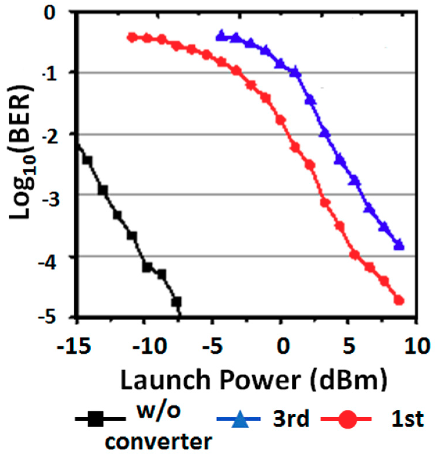
To demonstrate the operation of the ROT, experimental results in terms of bit error rate (BER) variation with ROP are presented in Figure 6. For the BER curves plotted in Figure 6a all parameters presented in Table 1 are adopted, with 16-QAM used on all employed subcarriers and a uniform subcarrier power loading profile is applied. The first five subcarriers of the quadrature channel are dropped, due to excessive BER levels induced by (i) frequency response ripples due to the low tap count, which are more pronounced at low frequencies in the quadrature-phase channel [20] and (ii) undesirable intermixing frequency products produced by square-law photon detection in the receiver which have higher powers at lower frequencies. The resulting raw line rate is 1.875 Gb/s (1.25 Gb/s) for the in-phase (quadrature) channel, thus the aggregated raw signal line rate is over the 25 km SSMF IMDD system is 3.125 Gb/s. This demonstrates that a single sub-wavelength channel is capable of supporting multi-Gb/s capacities. In comparison with the quadrature channel the in-phase channel achieves both a higher transmission capacity and a lower ROP at the adopted FEC limit of 1E-3, this is attributed to the fact that the in-phase channel has an inherently flat frequency response compared to the quadrature channel [20].
To explore the effect of the transceiver’s reconfigurability on system BER performances, Figure 6a also shows the BER performance for 25 km SSMF transmission of each channel whilst the other channel is disabled in the digital domain whilst preserving all other transceiver and system parameter settings. Figure 6a shows that, at the adopted FEC limit, the channel multiplexing and demultiplexing operation results in an increase of ~2 dB (~3 dB) in ROP for the quadrature (in-phase) channel. This ROP penalty is due to cross-channel interference (CCI) effects [21], however it is possible to eliminate this penalty by applying adaptive bit loading, although this incurs ~25% reduction in the maximum channel transmission capacities that can be achieved. To significantly reduce the CCI between orthogonal channels and so improve channel transmission performance, a DSP-based CCI cancellation (CCIC) technique has been demonstrated [21], under certain conditions the technique achieved a reduction in individual OFDM subcarrier BERs of more than 1000 times, an increase in transmission capacity by as much as 19 times and an increase in optical power budget by as much as 3.5 dB.
To explore the impact of the OFDM modulation’s adaptive bit loading feature, the BER versus ROP performance is plotted for each individual channel in Figure 6b with the transceiver parameters and system operating conditions identical to those employed in Figure 6a, except that now the capacity is maximised by applying adaptive bit loading (selecting subcarrier modulation from 16-QAM, 32-QAM or 64-QAM). In carrying out adaptive bit loading, the highest possible signal modulation format is selected first on the highest possible frequency subcarriers (as they exhibit better SNR) to maximise total transmission capacity whilst maintaining the total BER below the FEC limit of 1E-3. Figure 6b shows that the adaptive bit loading cannot only improve channel transmission capacity, but also reduce the associated power penalty. The optimized bit loading achieves a channel capacity of 2.03 Gb/s for the in-phase channel and 1.41 Gb/s for the quadrature channel with an aggregated capacity of 3.44 Gb/s for the entire 25 km SSMF IMDD system. Therefore, the aggregated transmission capacity has been increased by ~10%, due to the adaptive bit loading. This demonstrates that it is possible to exploit adaptive modulation to maximize transmission performance in a transmission system incorporating impairments associated with practical digital orthogonal filter implementations.
3.2. Soft-ROADMs
3.2.1. Operating Principle
A schematic diagram of the proposed soft-ROADM architecture is shown in Figure 7, which includes the channel add and drop functional elements. The solution fully supports SDN controllability, as shown in Figure 7. In the soft-ROADM, the input and output optical signals of each wavelength (in both east and west directions) consist of multiple sub-wavelength bands at different RF central frequencies generated within the ROTs, where, as described in Section 2.2, each individual sub-wavelength band can support one or two digital orthogonal filtering-enabled spectrally-overlapped sub-bands (I and Q) or a single sub-band (I or Q). For a specific optical carrier frequency, , the optical signal containing n sub-wavelength bands is expressed as:
where is the generated sub-band signal when the original base-band signal is up-sampled and subsequently filtered by the corresponding I or Q component of the i-th orthogonal digital filters in the ROTs.
As shown in Figure 7, to drop a targeted sub-band signal conveyed by a sub-wavelength band of a selected wavelength, the wavelength containing the targeted sub-band is directly inputted into an intensity modulator (IM) driven by a SDN-controlled drop RF signal having a sinusoidal waveform. The drop RF signal for the w-th sub-band and i-th sub-wavelength is expressed as:
where is the required IM bias voltage, A is the amplitude of the RF component of the drop RF signal and the digital filters’ central frequencies are positioned at (i = 1, 2, 3, 4, …, n). As the I and Q component of the w-th sub-band is orthogonal, they effectively have a phase difference of, this phase shift should be applied to the drop RF signal to select either the I or Q component in the drop operation, as shown in Equation (2). When both the frequency and phase of the drop RF signal match the targeted sub-band signal, the drop operation shifts the targeted sub-band to the baseband spectral region. At the IM output, the dropped sub-band with a reversed spectrum is shifted to the baseband spectral region, while all other sub-bands of the same wavelength are ruined and unrecoverable. After the direct detection of the dropped optical signal in a ROT, the receiving digital filter is configured as a simple baseband low-pass filter (suitable for use in all the drop operations) and is employed to select the dropped signal and remove the ruined and unrecoverable sub-bands. The values of and A can be adjusted for optimum transmission performance.
By simultaneously using I and Q drop RF signals in two parallel drop function elements, as indicated in Equation (2), a sub-wavelength level drop operation can also be performed. Furthermore, to drop an entire wavelength, the IM can be configured as an optical passway if the drop RF signal amplitude is set to zero (A = 0).
Here it is worth addressing that, an alternative approach for the soft-ROADM drop operation could involve splitting part of the signal power from the required optical wavelength, direct detection and A-D conversion of the entire band of channels and finally digital demultiplexing via a matching filter and down-sampling. To compare these two approaches, an IM is not needed in the alternative approach, however the big advantage of the IM-based approach over the alternative one is that the ROT only needs to operate at the bandwidth of the dropped sub-band which is usually only 1/100 to 1/10 of the aggregated wavelength channel in the CAN. This means far cheaper optical and electrical components with low-bandwidth can be used (particularly ADCs with a lower sampling rate) in the ROTs to significantly reduce the overall cost of the CAN deployment.
On the other hand, in the add functional element, similar to the procedure reported in [22], the add operation at a specific wavelength can be performed by passive optical coupling in an optical coupler (OC), as illustrated in Figure 7. Such an operation can be expressed as:
where and are the input and output optical signals of the add function element, and is the optical sub-band/sub-wavelength signal to be added. In the sub-wavelength-level add operation, a sufficient spacing [23] between the wavelengths of the two channels should be considered to avoid the optical beat interference (OBI) effect within the bandwidth of the receiver. In Equation (3) it is assumed that there is no OBI effect present. In the sub-wavelength and sub-band level add operation, to achieve the contention-free add operation, has to be located in a free location within the digital filtering space. This can be easily realized by selecting a free digital filter type (I and/or Q) for a given central RF frequency and/or shifting the central RF frequency of a digital filter having a specific type in the digital domain prior to performing the E-O conversion in the corresponding ROT [9].
The aforementioned soft-ROADM operations are fully controlled by a ROADM-embedded DSP controller, as shown in Figure 7, which determines the required set of dynamic operating parameters through regular communication with the centralised SDN controller via an extended OpenFlow protocol [24,25]. The dynamic parameter set may include digital filter characteristics employed by the targeted sub-bands/sub-wavelengths, characteristics of the drop RF signal when the drop operation is required and information on free filter locations in the digital filtering space when the add operation is required. As the parameter set can be dynamically generated and finely adjusted using DSP algorithms according to the prevailing tasks, traffic status and network characteristics, the operations of the proposed soft-ROADMs are thus flexible, scalable, adaptive and physical-layer network characteristic-transparent.
Here it is worth mentioning the following two aspects: (i) For a given wavelength in a network node, the dropped signals at specific sub-wavelengths and/or sub-bands are not erased from the original input wavelength before the add operation, as shown in Figure 7. As such, when the add operation is performed at the same wavelength, this may result in possible contention, whose probability, however, can be very low due as a relatively large digital filtering space would be adopted in practice; (ii) directionless operations can be achieved when the proposed ROADM is equipped with a typical CDC structure.
3.2.2. Soft-ROADM Experimental Demonstrations
The experimental system setup for the soft-ROADM add/drop operation is depicted in Figure 8, and the associated experimental system parameters are detailed in Table 2. The implemented system contains four channels, thus a single optical wavelength supports two Sub-λs at different centre frequencies (baseband BB and passband PB) each containing an orthogonal I and Q channels. These four channels are defined as BB-I, BB-Q, PB-I and PB-Q. Two 2-channel transmitters (Txs) are employed, each based on a software-configurable FPGA for DSP execution. Each FPGA generates and digitally adds two of the four channels. A 2 GS/s DAC supports a total signal bandwidth of 1 GHz, therefore Sub-λs are positioned at 0–0.5 GHz (BB) and at 0.5–1.0 GHz (PB). In the demonstration OFDM modulation is used on all channels, however, in theory, any signal modulation formats can be adopted. Sample timing synchronisation is achieved by delaying each RF signal appropriately via RF delay lines (DLs). To eliminate the OBI effect [23] associated with direct-detection (DD), the two employed laser sources have a 0.3 nm wavelength spacing. In Tx 1 the IM is an EML and in Tx 2 the IM is a tuneable laser source (TLS) and a Mach-Zehnder modulator (MZM). Erbium doped fibre amplifiers (EDFAs) followed by 0.8 nm OBPFs are used to equalize the optical launch powers. As shown in Figure 8, to configure the soft-ROADM add operation, the optical signals from Tx 1 and Tx 2 are passively combined in a 3 dB optical coupler (OC)-based soft-ROADM add element. The receiver (Rx) connects to the OC output port, where a variable optical attenuator (VOA) is used to adjust the ROP before O/E conversion with an integrated PIN and TIA, the generated RF signal amplitude is optimized by an RF amplifier and VEA before digitization by an ADC. The Rx FPGA then performs the required DSP functions for signal recovery. The Rx-DSP first performs MF-enabled Sub-B demultiplexing followed by OFDM demodulation to recover the PRBS data for subsequent BER analysis. To measure BERs before the add operation (BAD) both Txs are connected to the OC with their lasers on, but the FPGA’s digital signal output is only enabled in the transmitter to be measured, thus the associated laser will be unmodulated. This avoids optical power fluctuations induced by variations in optical fibre alignment in the connectors. BER measurements after the add operation (AAD) are made with both digital signals enabled simultaneously. To examine the soft-ROADM add performance for different channel add combinations, two different add cases are defined; (i) Sub-λ Add is BB-I + BB-Q optically added to PB-I + PB-Q, and (ii) Sub-B Add is BB-Q + PB-I optically added to BB-I + PB-Q.
To configure the soft-ROADM to perform the after drop (ADR) operation, the transmitter shown in Figure 8b, generates the PB Sub-λ comprising both I and Q Sub-Bs. Here an EDFA and OBPF are not necessary as the available optical power is sufficient and power balancing is not applicable. A drop element based on an MZM is employed in combination with a manually tuned LO to generate the required drop RF signal. To drop either PB-I or PB-Q, the RF drop signal’s frequency is set to 0.75 GHz (PB Sub-λ CF), the phase is adjusted to match that of the desired drop channel and the amplitude is optimised in order to minimize the drop channel’s BER. To recover the data from the baseband shifted Sub-B, firstly a digital LPF eliminates the unwanted residual sub-bands, then OFDM decoding is applied with subcarrier conjugation and order reversal included to compensate for the drop operation-induced spectral reversal, finally, BER analysis is performed. For the before drop (BDR) case, the drop element is bypassed, and data is recovery is identical to that in the BAD add case.
To allow acceptable BER levels for each Sub-B, the soft-ROADM add (drop) case employs the six (seven) highest frequency subcarriers out of 15 available. This is due to cross-channel interference (CCI) [21] occurring between orthogonal Sub-Bs with increasing interference levels at lower subcarrier frequencies. Figure 9a,b,d,e show the measured BAD and AAD BER curves for Sub-λ and Sub-B add operations respectively. The Sub-λ (Sub-B) add penalty for all channels is ≤1 dB (≤1.4 dB) at an FEC limit of 1E-3. The add penalties can be attributed to: (i) Residual CCI, (ii) finite tap length-induced non-perfect filter orthogonality and out-of-band attenuation, and (iii) DD-induced intermixing products. Figure 9c shows the BER curves for the BDR and ADR operations on PB-I and PB-Q. The BDR case has reduced sensitivity compared to the before Sub-λ add case due to the extra subcarrier employed. The soft-ROADM has a similar drop penalty for both channels of ~2 dB, which is mainly a result of signal distortions induced by the imperfect MZM-IM transfer function. In all cases, the Q channel performs slightly worse than the I channel due to the finite tap length-induced filter frequency response ripples being more prominent for the Q channels. Some examples of equalized and overlaid, subcarrier constellations at the receiver, are presented in Figure 9f–h for Sub-λ add (f), Sub-B add (g), and the drop operation (h).
3.3. Spectral Converters
3.3.1. Functionality and Operating Principle
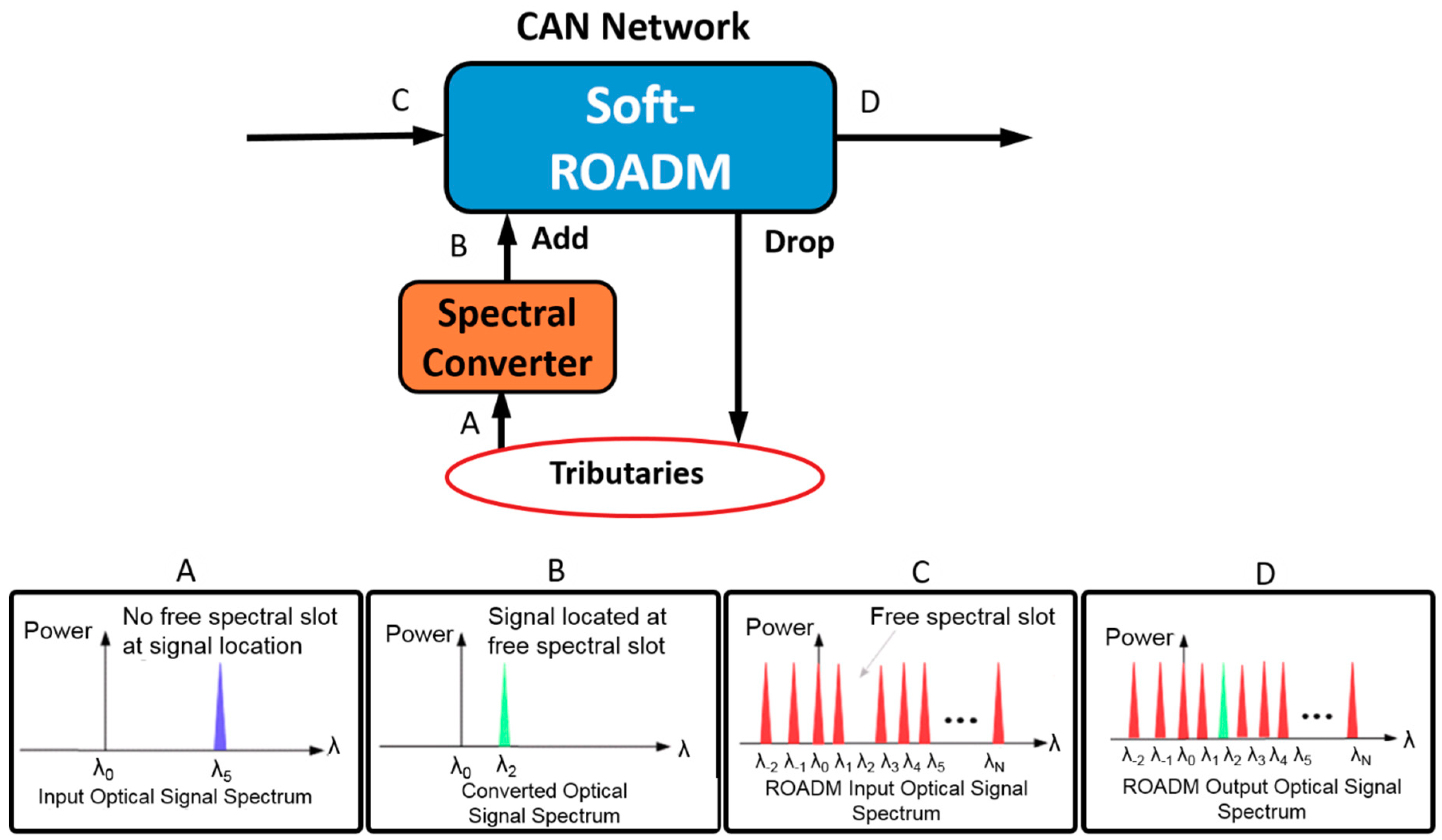
The basic signal spectral repositioning function of the spectral converter was outlined in Section 2.3, however, it is worth illustrating the basic functionality with a practical example of its application in a CAN. Figure 10 depicts an example of how the spectral converter can be utilized in conjunction with a soft-ROADM to increase traffic switching flexibility and reduce traffic blocking probability. The soft-ROADM is incorporated in the CAN and provides flexible connectivity to several network tributaries, such as PON connections, dedicated fixed data connections or mobile backhaul/fronthaul connections to a BBU/RRH. In the example, an upstream tributary is to be added to an aggregated signal in the CAN, however the spectral location of the tributary is occupied in the aggregated CAN signal, so it blocks the tributary from being directly added. Therefore, to avoid the traffic-blocking situation, which restricts the network’s flexibility, a spectral converter is employed to relocate the tributary to a free spectral location in the aggregated signal spectrum. The soft-ROADM can now perform a contention free add operation.
In Figure 11, the basic structure of the DSP-enabled spectral converter is illustrated. The operation of the spectral converter is based on a single standard dual-parallel Mach-Zehnder modulator (DP-MZM), comprising two parallel dual-drive Mach-Zehnder modulators (DD-MZMs), marked as MZ-a and MZ-b each driven by two RF driving signals and one DC bias voltage, and a phase modulator marked as MZ-c driven by a single DC bias voltage. The optical signal power input to the DP-MZM is equally split to feed MZ-a and MZ-b, each of the DD-MZMs converts its input signal to a set of optical components, which have a frequency spacing equal to the RF driving signal frequency, and with amplitudes and phases are governed by the Bessel function of the first kind. MZ-c is then used to control the phase difference between the two generated sets of frequency components, the two sets are then combined to generate an output signal containing the same set of frequency components, as shown in the output signal spectrum on the right of Figure 11. The generated set of optical components contains the same information within each optical component, however the power of each frequency components is dependent on the four RF driving signals and three DC bias voltages, which can be manipulated to control the distribution of power amongst the generated frequency components allowing maximisation of power at the desired frequency. The output optical signal is filtered by a tuneable optical filter to select the desired converted optical component and reject the unwanted optical components. Mathematical descriptions of the abovementioned processes are fully detailed in [11].
Two important characteristics of the spectral converter are spectral conversion efficiency and frequency detuning range. The conversion efficiency is defined as the optical power ratio between the desired output optical component and the input optical signal. Frequency detuning range is defined as the difference between the centre frequencies of the input optical signal and the desired output optical component, as shown in the output signal spectrum in Figure 11. It is easy to appreciate that the four RF driving signals and three DC bias voltages can be controlled to dynamically optimise the operating conditions of the spectral converter to simultaneously achieve three critical and complimentary performance criteria, which are (i) maximisation of the conversion efficiency of the desired optical component, (ii) an enhanced frequency difference between two adjacent converted optical components for a specific driving RF signal frequency and (iii) minimisation of the number of unwanted parasitic optical components. The optimum spectral converter operating conditions for a specific detuning range have been identified analytically in [11], where performance was also explored statistically using a wide range of randomly generated operating conditions in order to fully confirm the validity of the identified optimum operating conditions.
To control a spectral converter’s configuration in the dynamically reconfigurable CAN, the spectral converter would include an embedded DSP controller, which periodically communicates with a centralised SDN controller, via an extended OpenFlow protocol, in order to dynamically set and adjust the converter’s configuration. The centralised SDN controller would also exchanges control information with other DSP controllers embedded in other spectral converters, transceivers and soft-ROADMs to coordinate and manage the overall connectivity within the CAN. Therefore, the highly flexible spectral converters are fully compatible with SDN-controlled CAN network scenarios.
3.3.2. Experimental Analysis of Spectral Converter Performance
To verify the theoretically predicted performance [11], the spectral converter’s performance has been experimentally demonstrated when subject to varying operating conditions. The experiment employed a DP-MZM-based spectral converter system, as shown in Figure 11. The input optical signal was a 1550.118 nm continuous wave light source at a power of 13 dBm, which was intensity modulated via an MZM with a 10 Gb/s, 16-QAM, OFDM signal, generated via an arbitrary waveform generator (AWG). The modulated optical signal power first passed through an EDFA and a variable optical attenuator before injection into an integrated DP-MZM (12.5 dB insertion loss and 22 dB extinction ratio) where the output optical signal is subject to the spectral conversion effect. The RF driving signal is an amplified 12.5 GHz sinusoid, which is divided into four separate signals, each RF signal then passes through a phase shifter to independently control its phase, before it drives one of the four DP-MZM electrodes. According to the identified optimum operating conditions, the four RF driving signals must have the same amplitude, the required amplitude being determined by the order of the desired converted optical component. The phases of the four RF driving signals must also be adjusted for a spacing of 90°, thus the relative phases are 0°, 90°, 180° and 270°. The output optical signal containing the converted optical frequency components is then optically filtered by a tunable optical filter to select the desired optical component. The optical signal is subsequently directly-detected by a 12 GHz photodetector, the resultant electrical signal is digitized and captured by a digital storage oscilloscope (DSO) and offline processing then demodulates the signal and analyses its BER performance.
For a 7.9 dBm, 10 Gb/s OOFDM signal at the converters input, Figure 12a shows the unfiltered converted optical spectrum at the DP-MZM’s output, where the operating conditions have been optimized for the first spectral component giving a detuning range of 12.5 GHz. To show the effect of non-optimized operating conditions, Figure 12b shows the corresponding optical spectrum when the DC bias voltages are arbitrarily set and not optimized. It can be clearly seen that when optimized operating conditions are employed the power of the first spectral component is significantly enhanced whilst the power of the other spectral components is diminished. The experiment demonstrated that the optimum operating conditions reduced the power of 75% of the parasitic optical components to more than 35 dB below the power of the desired optical component. Furthermore, the experimentally measured conversion efficiency of −17.4 dB closely agreed with the theoretically predicted value.
For the first and third converted optical components, each obtained under its optimum operating conditions, BERs as a function of optical launch power are plotted in Figure 13, thus the spectral converter-induced power penalties are shown in relation to a spectral conversion-free optical signal. The spectral conversion induced power penalty at the FEC limit of 1E-3 is approximately 16.2 dB and 19.1 dB for the first and third converted optical components, respectively. The power penalties are due to the DP-MZM insertion loss effect and the frequency detuning range dependent conversion efficiency, thus the third converted optical component has a higher penalty, due to its higher frequency detuning range. Frequency detuning range-independent spectral conversion efficiency is however feasible by utilizing a variable driving RF frequency and keeping the targeted optical component index constant.
This first experimental demonstration of the recently proposed spectral converter clearly shows the technical viability of the spectral conversion technique.
4. Conclusions
This review paper has provided an overview of the general CAN concept and a summary of the recent DSP-based research work relating to the proposed CAN technology. The CAN is shown to exploit both DSP-based and DSP-enabled networking devices, to achieve a dynamically reconfigurable network with fine granularity, elastic bandwidth channels that can be multiplexed at the wavelength, sub-wavelength and orthogonal sub-band levels. The CAN realises a dynamic network that can seamlessly integrate Metro-networks, fixed access networks and 4G/5G mobile fronthaul and backhaul networks, thus significantly reducing the cost of network ownership. The adaptive characteristics of the CAN networks provide a cost-effective solution to the relentless growth in demand for data capacity by dynamically sharing and allocating network capacity on-demand to meet the prevailing network traffic requirements. Thus, by fully utilising the available network resources, the CAN removes the need to over provision fixed resources to meet the worst-case traffic scenarios. The CAN also fully supports SDN for efficient control and management of the whole network configuration, including the physical layer. Key DSP-based/enabled network devices that enable the CANs have been presented in terms of operating principles and experimental demonstrations, these network devices are DSP-based reconfigurable optical transceivers, DSP-enable soft-ROADMS and DSP-enabled spectral converters, all of which have been successfully demonstrated in proof-of-principle experiments, which confirms their technical viability.
To further develop and assess the presented CAN technologies our future research work will focus on aspects, such as, the practical real-time demonstration of CANs with increased channel count and increased aggregate bandwidth, demonstration of the CAN’s transparency to signal characteristics, such as modulation format, the impact of cascaded soft-ROADMs on CAN performance and DSP-based techniques to improve CANs in terms of reconfigurability, flexibility and transmission performance.
Author Contributions
R.G. supervised the work, provided technical guidance for the DSP design/implementation and wrote the paper; X.D. undertook all DSP-design and experimental work relating to reconfigurable optical transceivers; E.A.-R. undertook all DSP-design and experimental work relating to soft-ROADMs; M.M. undertook all simulation and experimental work relating to spectral converters.
Funding
The work on reconfigurable optical transceivers was supported by PIANO + under the European Commission’s ERA-NET Plus scheme within the project OCEAN under Grant agreement 620029. The work on soft-ROADMs was supported by The Ser Cymru National Research Network in Advanced Engineering and Materials (NRN024) and by the IRAQI Ministry of Higher Education and Scientific Research (MOHESR). The work on spectral converters was supported by The Ser Cymru National Research Network in Advanced Engineering and Materials (NRN024 and NRN147) and by the National Natural Science Foundation of China (Project No. 61132004, 61275073, and 61420106011).
Conflicts of Interest
The authors declare no conflict of interest. The founding sponsors had no role in the design of the study; in the collection, analyses, or interpretation of data; in the writing of the manuscript, and in the decision to publish the results.
References
- Dubey, N. From Static Networks to Software-driven Networks—An Evolution in Process. Available online: http://www.isaca.org/Journal/archives/2016/volume-4/Pages/from-static-networks-to-software-driven-networks-an-evolution-in-process.aspx (accessed on 14 November 2018).
- Ibe, O.C. Fundamentals of Data Communication Networks; Wiley: Hoboken, NJ, USA, 2017; ISBN 9781119436270. [Google Scholar]
- Predictions 2016: The Dawn of the Gigabit Internet Age: Every Bit Counts | Technology, Media, and Telecommunications. Available online: https://www2.deloitte.com/il/en/pages/technology-media-and-telecommunications/articles/tmt-pred16-telecomm-dawn-of-the-gigabit-internet-age.html (accessed on 27 September 2018).
- Zilberman, N.; Watts, P.M.; Rotsos, C.; Moore, A.W. Reconfigurable Network Systems and Software-Defined Networking. Proc. IEEE 2015, 103, 1102–1124. [Google Scholar] [CrossRef]
- Amin, R.; Reisslein, M.; Shah, N. Hybrid SDN Networks: A Survey of Existing Approaches. IEEE Commun. Surv. Tutor. 2018. [Google Scholar] [CrossRef]
- Duan, X.; Giddings, R.P.; Mansoor, S.; Tang, J.M. Experimental demonstration of upstream transmission in digital filter multiple access pons with real-time reconfigurable optical network units. J. Opt. Commun. Netw. 2017, 9, 45–52. [Google Scholar] [CrossRef]
- Jin, W.; Zhang, C.; Duan, X.; Kadhum, M.R.; Dong, Y.X.; Giddings, R.P.; Jiang, N.; Qiu, K.; Tang, J.M. Improved Performance Robustness of DSP-Enabled Flexible ROADMs Free from Optical Filters and O-E-O Conversions. J. Opt. Commun. Netw. 2016, 8, 521–529. [Google Scholar] [CrossRef]
- Bolea, M.; Giddings, R.P.; Tang, J.M. Digital Orthogonal Filter-Enabled Optical OFDM Channel Multiplexing for Software-Reconfigurable Elastic PONs. J. Light. Technol. 2014, 32, 1200–1206. [Google Scholar] [CrossRef]
- Bolea, M.; Giddings, R.P.; Bouich, M.; Aupetit-Berthelemot, C.; Tang, J.M. Digital filter multiple access PONs with DSP-enabled software reconfigurability. J. Opt. Commun. Netw. 2015, 7, 215–222. [Google Scholar] [CrossRef]
- Duan, X.; Giddings, R.; Bolea, M.; Ling, Y.; Mansoor, S.P.; Tang, J.M. Real-time Demonstrations of Software Reconfigurable Optical OFDM Transceivers Utilising DSP-based Digital Orthogonal Filters for Channel Multiplexing. In Proceedings of the Asia Communications and Photonics Conference ACP2014, Shanghai, China, 11–14 November 2014. [Google Scholar]
- Mao, M.Z.; Giddings, R.P.; Cao, B.Y.; Xu, Y.T.; Wang, M.; Tang, J.M. DSP-enabled reconfigurable and transparent spectral converters for converging optical and mobile fronthaul/backhaul networks. Opt. Express 2017, 25, 13836. [Google Scholar] [CrossRef] [PubMed]
- Yoo, S.J.B.; Caneau, C.; Bhat, R.; Koza, M.A.; Rajhel, A.; Ringo, J. Progress in wavelength conversion by difference-frequency generation in AlGaAs waveguides. In Proceedings of the 1997 Digest of the IEEE/LEOS Summer Topical Meeting: Vertical-Cavity Lasers/Technologies for a Global Information Infrastructure/WDM Components Technology/Advanced Semiconductor Lasers and Applications/Gallium Nitride Materials, Processing, and Devices, Montreal, QC, Canada, 11–13 August 1997; pp. 36–37. [Google Scholar]
- Nguyen, A.; Porzi, C.; Serafino, G.; Fresi, F.; Contestabile, G.; Bogoni, A. All-Optical Gated Wavelength Converter-Eraser Using a Single SOA-MZI. IEEE Photonics Technol. Lett. 2011, 23, 1621–1623. [Google Scholar] [CrossRef]
- Dorward, R.M.; Anderson, M.J.; Giddings, R.P. Technical and market feasibility of high-speed software-reconfigurable OOFDM/DFMA-based Optical transceivers for Next Generation Access Network PONs. In Proceedings of the International Conference on Transparent Optical Networks, Trento, Italy, 10–14 July 2016. Paper Th.B1.4. [Google Scholar]
- Al-Rawachy, E.; Giddings, R.P.; Tang, J.M. Experimental demonstration of real-time add/drop operations in DSP-enabled flexible ROADMs for converging fixed and mobile networks. In Proceedings of the Optical Fiber Communication Conference (OFC), San Diego, CA, USA, 11–15 March 2018. Paper W2A.33. [Google Scholar]
- Duan, X.; Giddings, R.P.; Mansoor, S.; Tang, J.M. Performance Tolerance of IMDD DFMA PONs to Channel Frequency Response Roll-off. IEEE Photonics Technol. Lett. 2017, 29, 1655–1658. [Google Scholar] [CrossRef]
- Giddings, R.P.; Jin, X.Q.; Hugues-Salas, E.; Giacoumidis, E.; Wei, J.L.; Tang, J.M. Experimental demonstration of a record high 11.25 Gb/s real-time optical OFDM transceiver supporting 25 km SMF end-to-end transmission in simple IMDD systems. Opt. Express 2010, 18, 5541–5555. [Google Scholar] [CrossRef] [PubMed]
- Giddings, R.P.; Hugues-Salas, E.; Tang, J.M. Experimental demonstration of record high 19.125 Gb/s real-time end-to-end dual-band optical OFDM transmission over 25 km SMF in a simple EML-based IMDD system. Opt. Express 2012, 20, 20666–20679. [Google Scholar] [CrossRef] [PubMed]
- Jin, X.Q.; Wei, J.L.; Giddings, R.P.; Tang, J.M.; Quinlan, T.; Walker, S. Experimental Demonstrations and Extensive Comparisons of End-to-End Real-Time Optical OFDM Transceivers With Adaptive Bit and/or Power Loading. IEEE Photonics J. 2011, 3, 500–511. [Google Scholar] [CrossRef]
- Duan, X.; Giddings, R.P.; Bolea, M.; Ling, Y.; Cao, B.; Mansoor, S.; Tang, J.M. Real-time experimental demonstrations of software reconfigurable optical OFDM transceivers utilizing DSP-based digital orthogonal filters for SDN PONs. Opt. Express 2014, 22, 19674–19685. [Google Scholar] [CrossRef] [PubMed]
- Al-Rawachy, E.; Giddings, R.P.; Tang, J.M. Experimental demonstration of a DSP-based cross-channel interference cancellation technique for application in digital filter multiple access PONs. Opt. Express 2017, 25, 3850. [Google Scholar] [CrossRef] [PubMed]
- Jin, W.; Duan, X.; Dong, Y.; Cao, B.; Giddings, R.P.; Zhang, C.; Qiu, K.; Tang, J.M. DSP-Enabled Flexible ROADMs Without Optical Filters and O-E-O Conversions. J. Light. Technol. 2015, 33, 4124–4131. [Google Scholar] [CrossRef]
- Jin, X.Q.; Groenewald, J.; Hugues-Salas, E.; Giddings, R.P.; Tang, J.M. Upstream power budgets of IMDD optical OFDMA PONs incorporating RSOA intensity modulator-based colorless onus. J. Light. Technol. 2013, 31, 1914–1920. [Google Scholar] [CrossRef]
- Cvijetic, N. Software-defined optical access networks for multiple broadband access solutions. In Proceedings of the Opto-Electronics and Communications Conference (OECC), Kyoto, Japan, 30 June–4 July 2013. Paper TuP2-1. [Google Scholar]
- Cvijetic, K.S.N.; Tanaka, A.; Ji, P.N.; Murakami, S.; Wang, T. First OpenFlow-based software-defined λ-Flow architecture for flex-grid OFDMA mobile backhaul over passive optical networks with filterless direct detection ONUs. In Proceedings of the Optical Fiber Communication Conference (OFC), Anaheim, CA, USA, 17–21 March 2013. Paper PDP5B.2. [Google Scholar]
Figure 1.
Digital orthogonal filtering-based channel multiplexing: SF, shaping filter; DAC, digital to analogue converter; IM, intensity modulator; ADC, analogue to digital converter; MF, matching filter; M↑, up-sampling by factor M; M↓, down-sampling by factor M.
Figure 1.
Digital orthogonal filtering-based channel multiplexing: SF, shaping filter; DAC, digital to analogue converter; IM, intensity modulator; ADC, analogue to digital converter; MF, matching filter; M↑, up-sampling by factor M; M↓, down-sampling by factor M.
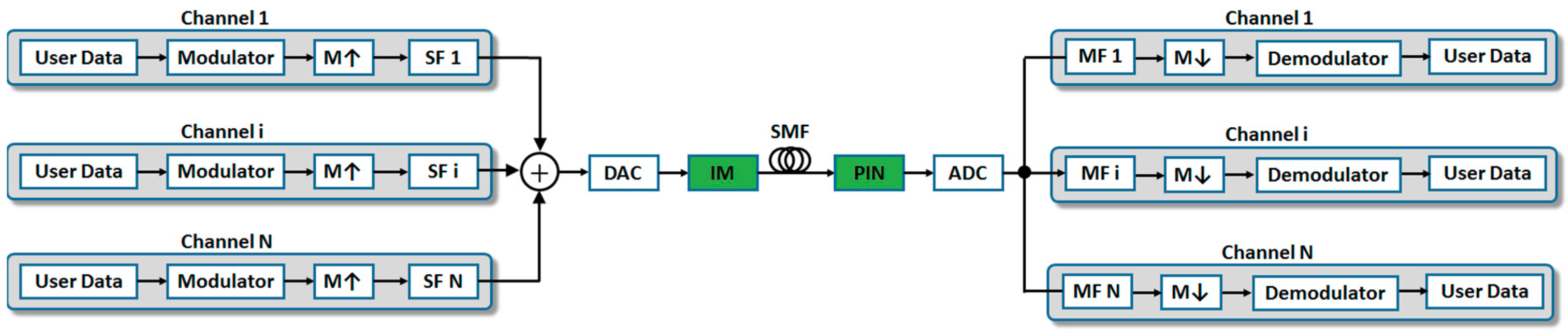
Figure 2.
Example electrical spectra of combinations of digital orthogonal filter multiplexed channels. (a) Equal bandwidth channels; (b) varying bandwidth channels.
Figure 2.
Example electrical spectra of combinations of digital orthogonal filter multiplexed channels. (a) Equal bandwidth channels; (b) varying bandwidth channels.

Figure 3.
Cloud Access Network (CAN) Architecture.

Figure 4.
Two Channel reconfigurable optical transceiver digital signal processing (DSP) architecture. JTAG, Joint Test Action Group; FIR, finite impulse response; FPGA, field programmable gate array.
Figure 4.
Two Channel reconfigurable optical transceiver digital signal processing (DSP) architecture. JTAG, Joint Test Action Group; FIR, finite impulse response; FPGA, field programmable gate array.

Figure 5.
Reconfigurable optical transceiver real-time experimental system setup. FEA, fixed electrical attenuator; PIN + TIA, integrated photodetector and transimpedance amplifier.
Figure 5.
Reconfigurable optical transceiver real-time experimental system setup. FEA, fixed electrical attenuator; PIN + TIA, integrated photodetector and transimpedance amplifier.

Figure 6.
BER vs. received optical power. (a) Identical modulation of 16-QAM on all subcarriers of each channel. (b) Adaptive subcarrier bit loading applied on each channel. (Channel 1: In-phase, Channel 2: Quadrature).
Figure 6.
BER vs. received optical power. (a) Identical modulation of 16-QAM on all subcarriers of each channel. (b) Adaptive subcarrier bit loading applied on each channel. (Channel 1: In-phase, Channel 2: Quadrature).

Figure 7.
Architecture of DSP-enabled soft-reconfigurable optical add/drop multiplexer (soft-ROADM).
Figure 7.
Architecture of DSP-enabled soft-reconfigurable optical add/drop multiplexer (soft-ROADM).

Figure 8.
Soft-ROADM add and drop operations experimental system setup. (a) Transmitter system for add operations; (b) transmitter system for drop operation; (c) add element; (d) drop element; and (e) receiver system.
Figure 8.
Soft-ROADM add and drop operations experimental system setup. (a) Transmitter system for add operations; (b) transmitter system for drop operation; (c) add element; (d) drop element; and (e) receiver system.
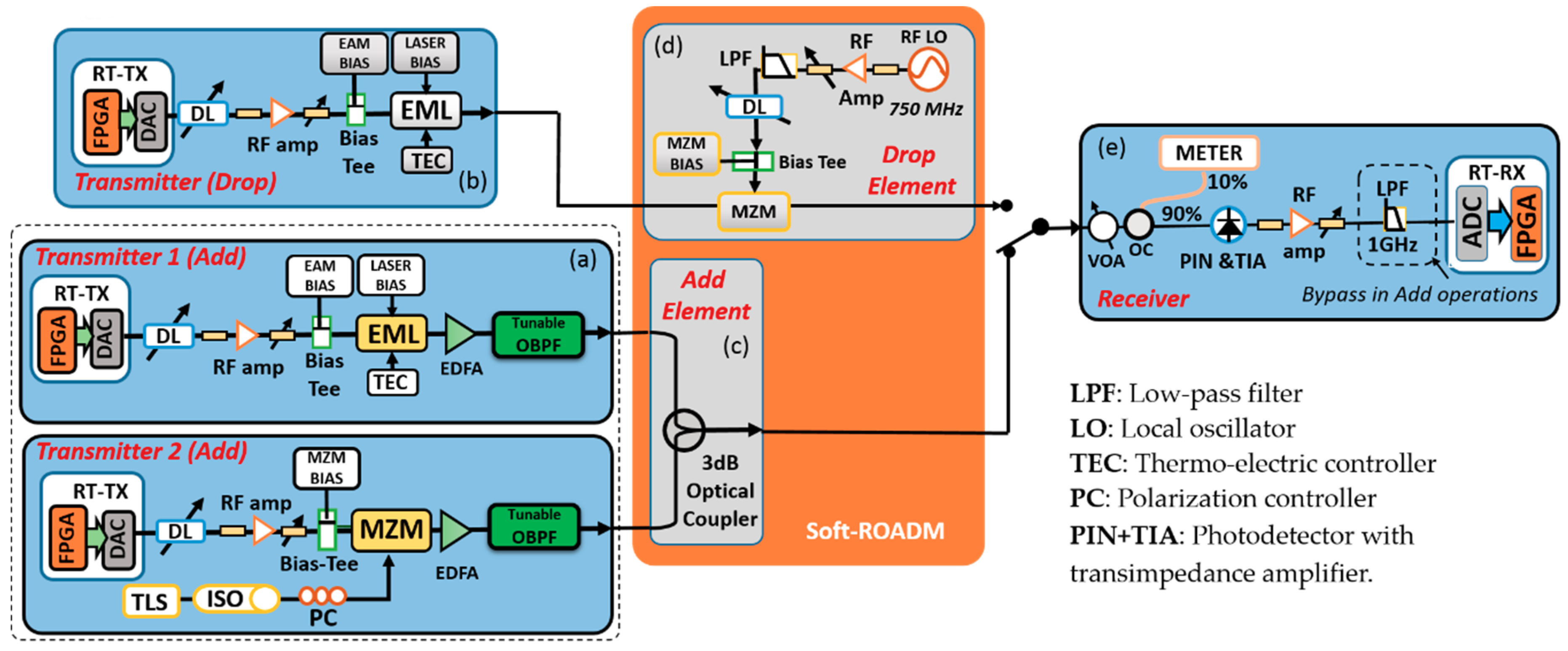
Figure 9.
BER curves for (a,b) each Sub-B before/after Sub-λ add; (c,d) each Sub-B before/after Sub-B add; (e) before/after the drop operation; Example subcarrier constellations at −18 dBm for the BB-I (upper) and PB-I (lower) after (f) Sub-λ add; (g) after Sub-B add; example subcarrier constellations at −14 dBm after the drop operation for (h) PB-I (upper) and PB-Q (lower).

Figure 10.
Example of spectral converter application in a CAN. (Insets shows spectra at indicated ports).
Figure 10.
Example of spectral converter application in a CAN. (Insets shows spectra at indicated ports).

Figure 11.
Spectral converter structure.
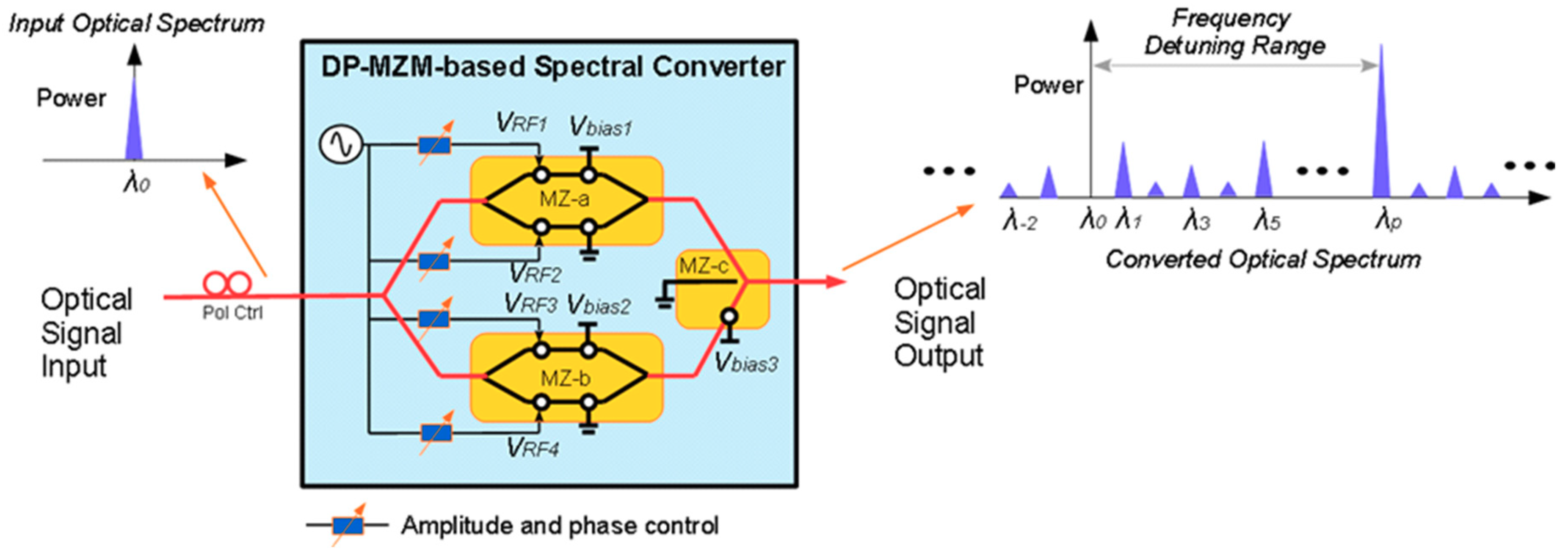
Figure 12.
Representative optical spectrum (a) emerging from the DP-MZM subject to the optimum operating conditions for the 1-st converted optical component; (b) emerging from the DP-MZM subject to non-optimized operating conditions.
Figure 12.
Representative optical spectrum (a) emerging from the DP-MZM subject to the optimum operating conditions for the 1-st converted optical component; (b) emerging from the DP-MZM subject to non-optimized operating conditions.
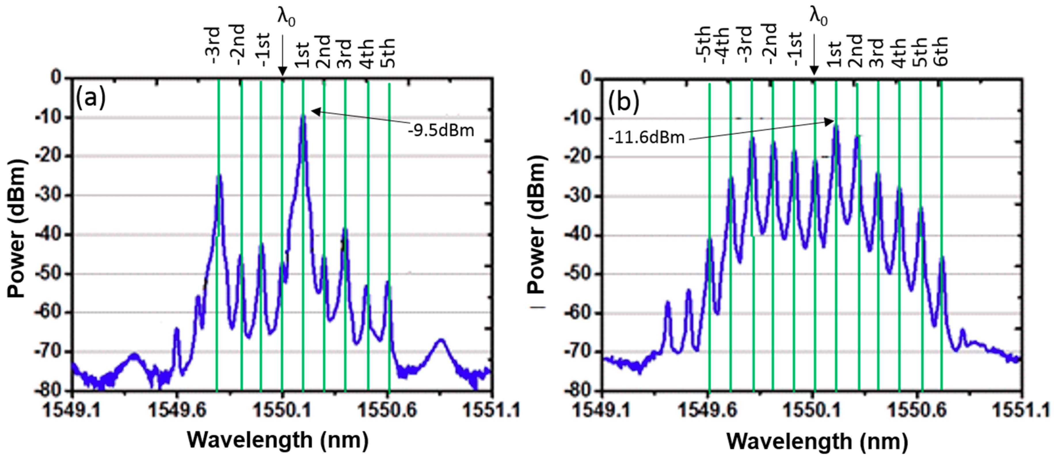
Figure 13.
BERs versus optical launch power for the first and third converted optical components each obtained under its optimum operating conditions. A BER curve for the spectral conversion-free input optical signal is also plotted for comparison.
Figure 13.
BERs versus optical launch power for the first and third converted optical components each obtained under its optimum operating conditions. A BER curve for the spectral conversion-free input optical signal is also plotted for comparison.

Table 1.
Experimental transceiver and system parameters.
| Parameter | Value | Parameter | Value |
|---|---|---|---|
| Total no. of IFFT/FFT points per channel | 32 | Total samples per symbol | 40 samples (20 ns) # |
| Data-carrying subcarriers per channel | 15 maximum | Error count period | 88,500 symbols |
| n-th subcarrier frequency | n × 31.25 MHz | EML laser wavelength | 1550 nm |
| Adaptive modulation formats | 16/32/64-QAM | 3 dB EML modulation bandwidth | 10 GHz |
| DAC and ADC sample rate/resolution | 2 GS/s/8 bits | Laser bias current | 124 mA |
| Symbol rate | 50 MHz | EAM bias voltage/driving voltage | −0.7 VDC/320 mVpp |
| Samples per symbol (IFFT) | 32 samples (16 ns) # | PIN detector bandwidth | 12.4 GHz |
| Cyclic prefix | 8 samples (4 ns) # | PIN detector sensitivity | −19 dBm * |
# Before up-sampling and after down-sampling; * Corresponding to 10 Gb/s non-return-to-zero data at a bit error rate (BER) of 1.0 × 10⁻⁹. FFT, fast Fourier transform; IFFT, inverse FFT; QAM, quadrature amplitude modulation.
Table 2.
Transceiver and system parameters.
| Parameter | Value |
|---|---|
| add/drop data-carrying subcarriers per sub-band | 6/7 |
| OFDM modulation format | 16-QAM |
| DAC and ADC sample rate/bit resolution | 2 GHz /8 bits |
| add/drop per channel raw bit rates | 0.3/0.35 Gb/s |
| Samples per symbol * IFFT/Cyclic prefix/Total | 32/8/40 Samples |
| EML wavelength/modulation bandwidth | 1550 nm/10 GHz |
| EML laser bias current/EAM bias voltage | 124 mA/−0.75 V |
| EML/MZM driving voltage Sub-λ add operation | 2.3/1.0 Vpp |
| EML/MZM driving voltage Sub-B add | 2.3/0.6 Vpp |
| MZM DC bias Sub-λ/Sub-B add operation | 1.3/1.47 V |
| MZM modulation bandwidth | 20 GHz |
| PIN sensitivity #/Bandwidth | −19 dBm/12.4 GHz |
| Add/Drop optical launch power | 4.5/3.1 dBm |
| Electrical signal amplitude at ADC | 300 mVpp |
| EML/MZM driving voltage drop operation | 2.3/3 Vpp |
| MZM DC bias drop operation | 1 Vpp |
* Before up-sampling and after down sampling; # Corresponding to 10 Gb/s NRZ data at a BER of 1.0 × 10⁻⁹.
© 2018 by the authors. Licensee MDPI, Basel, Switzerland. This article is an open access article distributed under the terms and conditions of the Creative Commons Attribution (CC BY) license (http://creativecommons.org/licenses/by/4.0/).
Share and Cite
MDPI and ACS Style
Giddings, R.; Duan, X.; Al-Rawachy, E.; Mao, M. A Review of DSP-Based Enabling Technologies for Cloud Access Networks. Future Internet 2018, 10, 109. https://doi.org/10.3390/fi10110109
AMA Style
Giddings R, Duan X, Al-Rawachy E, Mao M. A Review of DSP-Based Enabling Technologies for Cloud Access Networks. Future Internet. 2018; 10(11):109. https://doi.org/10.3390/fi10110109
Chicago/Turabian StyleGiddings, Roger, Xiao Duan, Ehab Al-Rawachy, and Mingzhi Mao. 2018. "A Review of DSP-Based Enabling Technologies for Cloud Access Networks" Future Internet 10, no. 11: 109. https://doi.org/10.3390/fi10110109
Note that from the first issue of 2016, this journal uses article numbers instead of page numbers. See further details here.