Article

Correlation between the Experimental and Theoretical Photoelectrochemical Response of a WO3 Electrode for Efficient Water Splitting through the Implementation of an Artificial Neural Network

1
Nanomaterials and Systems for Renewable Energy Laboratory, Research and Technology Center of Energy (CRTEn), Technoparc Borj Cedria, B.P. 095, Hammam Lif 2050, Tunisia
2
Faculty of Sciences of Sfax, University of Sfax, Soukra Road km 3.5, B.P. 1171, Sfax 3029, Tunisia
3
Faculty of Sciences of Tunis, University of Tunis El Manar, B.P. n° 94, Tunis 1068, Tunisia
4
Center of Physics and Engineering of Advanced Materials, Laboratory for Physics of Materials and Emerging Technologies, Chemical Engineering Department, Instituto Superior Técnico, Universidade de Lisboa, 1049-001 Lisbon, Portugal
*
Authors to whom correspondence should be addressed.
Sustainability 2023, 15(15), 11751; https://doi.org/10.3390/su151511751
Submission received: 20 June 2023 / Revised: 20 July 2023 / Accepted: 26 July 2023 / Published: 30 July 2023

Abstract

:
Since the discovery of photoelectrochemical (PEC) water splitting with titanium dioxide electrodes in the presence of ultraviolet light, much work has been conducted to build an effective PEC water splitting system and develop novel photoelectrodes. Using a facile and controllable electrodeposition method, a thin tungsten trioxide (WO3) film electrode onto a stainless steel (SS) substrate was synthetized. The effect of the deposition time on the structural, morphological, optical, and electrical properties of the as-grown WO3 thin films was assessed. XRD spectra of the obtained films reveal the polycrystalline nature of WO3 with a triclinic phase and exhibit a sharp transition to the (002) plane when the deposition time was extended beyond 10 min. The surface morphology showed a remarkable change in the grain size, thickness, and surface roughness when varying the deposition time. UV–Vis spectrophotometry revealed that the optical band gap values of WO3 decreased from 1.78 to 1.36 eV by extending the electrodeposition duration from 10 to 30 min, respectively. Notably, as indicated from the PEC measurements, the obtained photoelectrode exhibited the effects of the deposition time on the photocurrent density, and the maximum value obtained was around 0.07 mA cm−2 for the sample deposited at 10 min. Finally, this study presents for the first time an artificial neural network model to predict the PEC behavior of the prepared photoanode, with a highly satisfactory performance of less than 0.05% error. The low cost and simply synthetized WO3/SS electrode with superior electrochemical performance and the excellent correlation between the experimental and theoretical results demonstrate its potential for practical application in water splitting and hydrogen production.

Graphical Abstract

1. Introduction

Since the original work of Honda and Fujishima in 1972 [1], photoelectrochemical (PEC) water splitting has been regarded as one of the most promising ways to store solar energy and has attracted great levels of attention for nearly four decades. Generally, the PEC water splitting mechanism is based on generating photo-excited charge carriers. It consists of generating electron–hole pairs after light irradiation of a semiconductor-based photoanode [2]. Therefore, the big challenge remains to increase the charge separation and facilitate carrier mobility to obtain a better carrier collection efficiency. In this context, several studies have extensively focused on metal oxide semiconductors, such as TiO2 [3], ZnO [4], Fe2O3 [5], BiVO4 [6], Cu2O [7], and WO3 [8], as photoelectrodes in the PEC system. Among these metal oxides, tungsten trioxide (WO3) brings new opportunities for developing a PEC water splitting system with a superior performance [2]. This material has a band gap energy of about 2.5–2.7 eV, which is suitable for the redox potential of water decomposition. In addition, WO3 is characterized by a high crystallinity, a good porosity, a moderate hole diffusion length, the ability to capture 12% of the solar illumination, a good chemical stability, as well as easy and low-cost preparation methods [8]. Many modification strategies, for instance, metal element doping, composites, combination with two or three semiconductors (heterojunction), morphology modification, and the nature of the substrate, have been adopted to improve the PEC performance of WO3 semiconductors [8].
For example, Kalanur demonstrated a promising approach to enhance PEC water splitting efficiency through substitutional doping of a WO3 photoanode [9]. On the other hand, Kalanoor et al. reviewed the significant factors that influence the PEC activity of combining WO3 with BiVO4 [10]. Zhu et al. critically reviewed nanostructured WO3 synthesized through the electrochemical route for PEC water splitting [11]. Conventionally, PEC systems are usually investigated and developed on transparent conducting oxides (TCOs) supported on glass, such as fluorine-doped tin oxide, tin-doped indium oxide, etc. These substrates have been widely employed in PEC studies for photovoltaic and hydrogen generation applications. However, the relatively high sheet resistance (10–15 Ω/sq) and fragileness of glass-supported TCO substrates are the obstacles to producing large-area PEC cells. In addition, these TCO substrates are very expensive and represent about 40–60% of the cost of the devices themselves [12]. For practical applications, porous or wire-based electrode structures and lower-cost substrates are highly desirable, including those based on traditional engineering materials, such as stainless steel substrates. Stainless steel (SS) substrates are inexpensive, easily available, relatively more conducting, flexible, and corrosion resistant under aqueous solutions. High-temperature sintering can also be possible with such substrates [13]. In this context, WO3 on SS substrates is readily formed. For example, multilayered WO3 films have been successfully synthesized onto the large area sheet (9 × 9 cm2) and mesh (1 × 20 cm2) SS substrates using screen printing and brush painting methods, respectively. The authors of [12] have also demonstrated that enhancing the photocurrent of WO3 photoanodes coated on a SS mesh is associated with their large effective surface area. However, to the best of their knowledge, no reports have focused on the influence of the deposition time on the WO3 films electrodeposited onto the SS substrate, which has enticed a great level of interest in the industrial frame due to its excellent resistance to degradation, mainly in hydrogen production application via water splitting. Lamouchi et al. demonstrated that the photocurrent response of ZnO nanowires electrodeposited onto a stainless steel substrate is higher than those of the same materials deposited onto other substrates (e.g., ITO, quartz, glass, and sapphire) [14].
Many parameters affect the PEC performance of WO3 as a photoelectrode for hydrogen production. Therefore, a useful approach is the use of mathematical models for the inducement of the H2 product. For this purpose, several studies have been used, such as the artificial neural network (ANN), as a robust tool that can be applied to experimental data. ANNs are a learning system based on a computational technique that can simulate the neurological processing ability of the human brain. They can be applied to quantify a non-linear relationship between the causal factors and the response by means of iterative training of the data obtained from a designed experiment [15]. Compared with classical modeling techniques, such as the response surface methodology (RSM), ANNs show superiority as a modeling technique for datasets exhibiting non-linear relationships, and thus for both data fitting and prediction abilities [16]. They are adaptable and can be used to solve important engineering problems, including photocatalytic processes [17,18,19,20], supercapacitor applications [21,22,23], and water splitting [24,25,26]. In this context, Wang and colleagues have successfully built a machine learning (ML) model to predict the doping effect of 17 metal dopants into hematite (Fe2O3), a prototype photoelectrode material [27]. However, for inorganic semiconductor-based solar-driven water splitting, especially via the PEC process, there have been no attempts made to apply a ML model in addressing the research challenges of navigating a vast array of chemical and processing space. The ML model requires no prior domain knowledge to achieve a converged fitting model between the descriptors and the final outputs. With a sufficient database, it can identify the most significant parameters among the different system features. This benefit makes this technique particularly appealing in investigating dopant selection, which traditionally relies on a tremendous amount of random trials, offering a new pathway to guide the rational design of future material synthesis and their PEC property optimization.
Despite the numerous investigations employing ANNs or BP models to forecast the performance of materials as electrodes for renewable energy applications, there is only a relatively limited literature available on predicting the performance of WO3 thin films deposited by electrodeposition onto stainless steel electrodes. The novelty of this work resides in the fact that no prior studies have been conducted on the PEC response of WO3 photoanodes coated on SS substrates using the simple and inexpensive electrodeposition technique. In addition, due to their notable performance and cost-effectiveness, scaling devices made with SS substrates can be easily commercialized. In this work, WO3 thin films were grown using the electrodeposition technique onto a SS substrate with a deposition time ranging from 5 to 30 min, respectively. The deposition time was varied to optimize WO3 thin films’ physical and especially electrical properties. The enhanced PEC performance of the WO3 photoanode has been investigated and discussed in detail. Finally, the PEC performance of WO3/SS at an optimum deposition time was predicted using the ANN model, and the obtained results were compared to the experimental data.

2. Materials and Methods

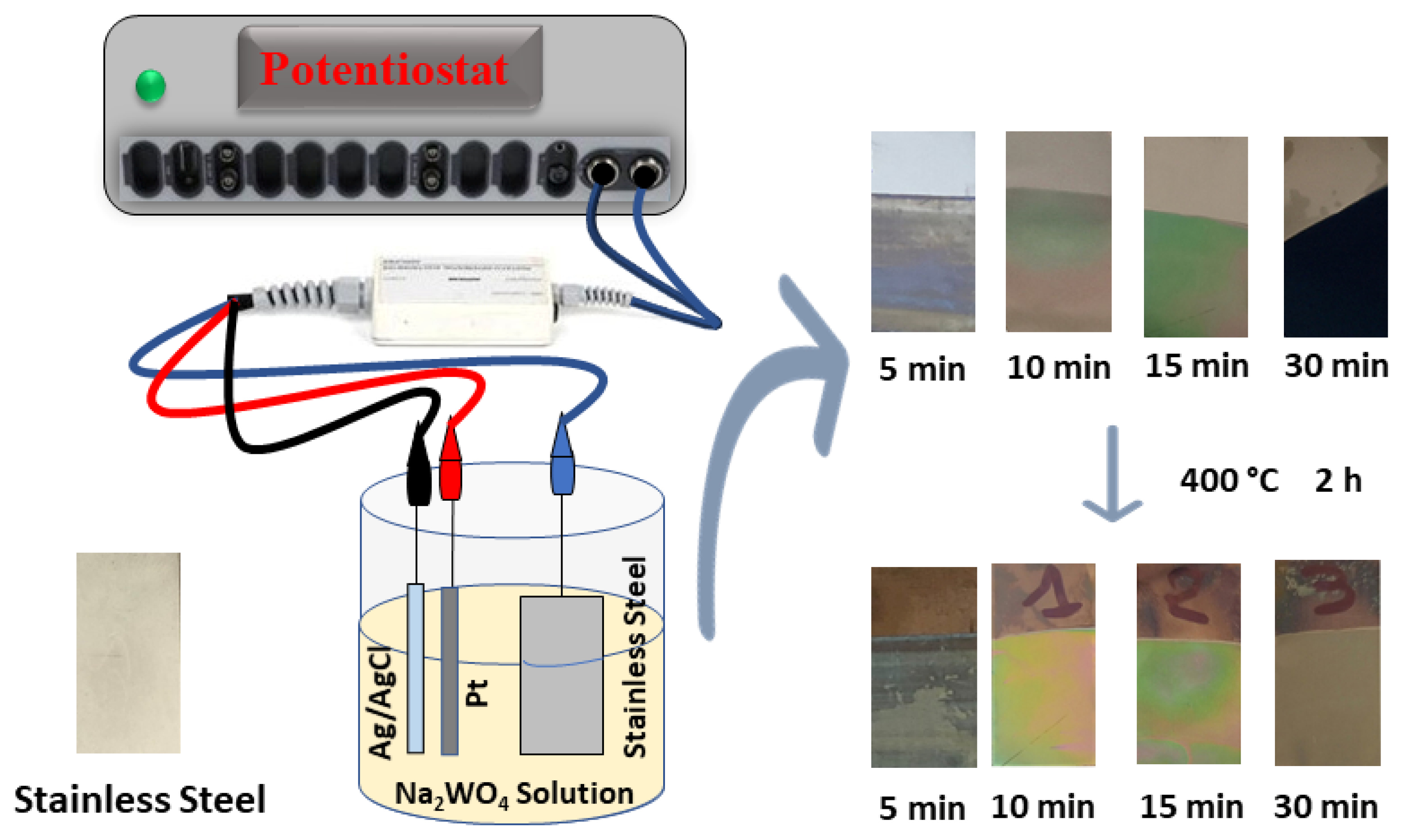
2.1. Preparation of WO3 Thin Films

All chemicals were of analytical reagent grade, purchased from Sigma-Aldrich, and used without further purification. Stainless steel 304 L, purchased from Laser Industry (Mégrine, Tunisia), was used as a substrate for elaborating WO3 thin films with the electrodeposition technique. Prior to its use, and to remove any rust, the substrate was cut into a rectangular shape with dimensions of 1 cm × 3 cm and 0.8 mm diameter, and then immersed in sulfuric acid (10%) for 2 min. Following this step, it was ultrasonically cleaned for 10 min in acetone, then in isopropanol, and rinsed with deionized water. Finally, the stainless steel substrate was dried in air at room temperature. Inspired by the work of Reyes-Gil et al. [28], WO3 thin films were deposited onto the SS substrate via the electrochemical deposition technique. The electrolyte solution was prepared using Na2WO4 (25 mM) as a precursor of tungsten, and H2O2 (30 mM), which can bind to the anion and improve its solubility under a low pH. The pH of the solution was about 10.4. To adjust the pH to 1.4, nitric acid was added subsequently. The synthesis process was conducted in a standard three-electrode system using a SOLARTRON analytical electrochemical workstation (Modulab Xm) potentiostat/galvanostat. The working electrode was the stainless steel substrate (SS 304 L), while the counter and the reference electrodes were a Pt wire and an Ag/AgCl electrode, respectively. Figure 1 illustrates the process by which the WO3 films were obtained at an optimized cathodic potential of −0.45 V (vs. Ag/AgCl). The deposition time was varied between 5 min, 10 min, 15 min, and 30 min, respectively, to tune the WO3 layer thickness. After each deposition, the samples were taken out of the solution, washed several times with distilled water, and then annealed in a muffle furnace at 400 °C for 2 h.

2.2. Sample Characterization

The X-ray diffraction (XRD) patterns of the electrodeposited WO3 films were obtained on a Bruker ADVANCE D8 diffractometer (Bruker Inc., Billerica, MA, USA) with the Bragg–Brentano configuration using CuKα radiation (λ = 1.54178 Å) at 40 kV and 40 mA. A scan rate of 3° min−1 was applied to record the XRD patterns in the angular range of (20° ≤ 2θ ≤ 70°) with a step size of 0.02°. The morphology of the samples was analyzed using scanning electron microscopy (SEM, JEOL JSM-96700, Peabody, MA, USA) with an accelerating voltage of 15 kV. The elemental composition was obtained using an energy-dispersive X-ray spectrometer (EDX). The optical measurements were deduced from UV–visible diffuse reflectance spectra recorded using a PerkinElmer Lambda 950 spectrophotometer (Shelton, CT, USA) in the 200–800 nm wavelength range at room temperature. Electrochemical impedance spectroscopy (EIS) measurements were performed using a SOLARTRON frequency response analyzer coupled to a ModuLab XM potentiostat/galvanostat in potentiostatic mode (AMETEK SI, Oak Ridge, TN, USA). A 10 mV amplitude sinusoidal signal was used and the frequencies ranged from 100 kHz to 0.01 Hz. A solution of 1 M KOH was used as an electrolyte at room temperature. The fitting of the obtained results in the EIS measurements and the equivalent circuit were performed using the Zview 4.0 software command.
Finally, the PEC performance of the WO3/SS thin film photoanodes was evaluated using a typical three-electrode quartz cell with the as-prepared WO3/SS samples as the working electrode (WE), Pt wire as the counter electrode (CE), and Ag/AgCl 3 M KCl from Metrohm (6.0733.100) as the reference electrode, respectively. A solution of Na2SO4 (0.5 M, pH = 7) was used as an electrolyte. The photoelectrode with an emerged surface of 1 cm2 was illuminated using a 300 W Xe arc lamp (100 mW cm−2). The intensity of the incident light from the Xe lamp was measured using a photometer Model 70,310 purchased from Spectra-Physics. The photo-response of all samples was evaluated through current–voltage (I–V) characteristic curves recorded using linear sweep voltammetry (LSV) at a scan rate of 10 mV s−1, with an applied potential varying from −1 V to 0.8 V vs. Ag/AgCl. The current–time (I–t) response of the samples was evaluated through chronoamperometry measurements that were carried out at 0.5 V vs. Ag/AgCl over continuous light on–off cycles.

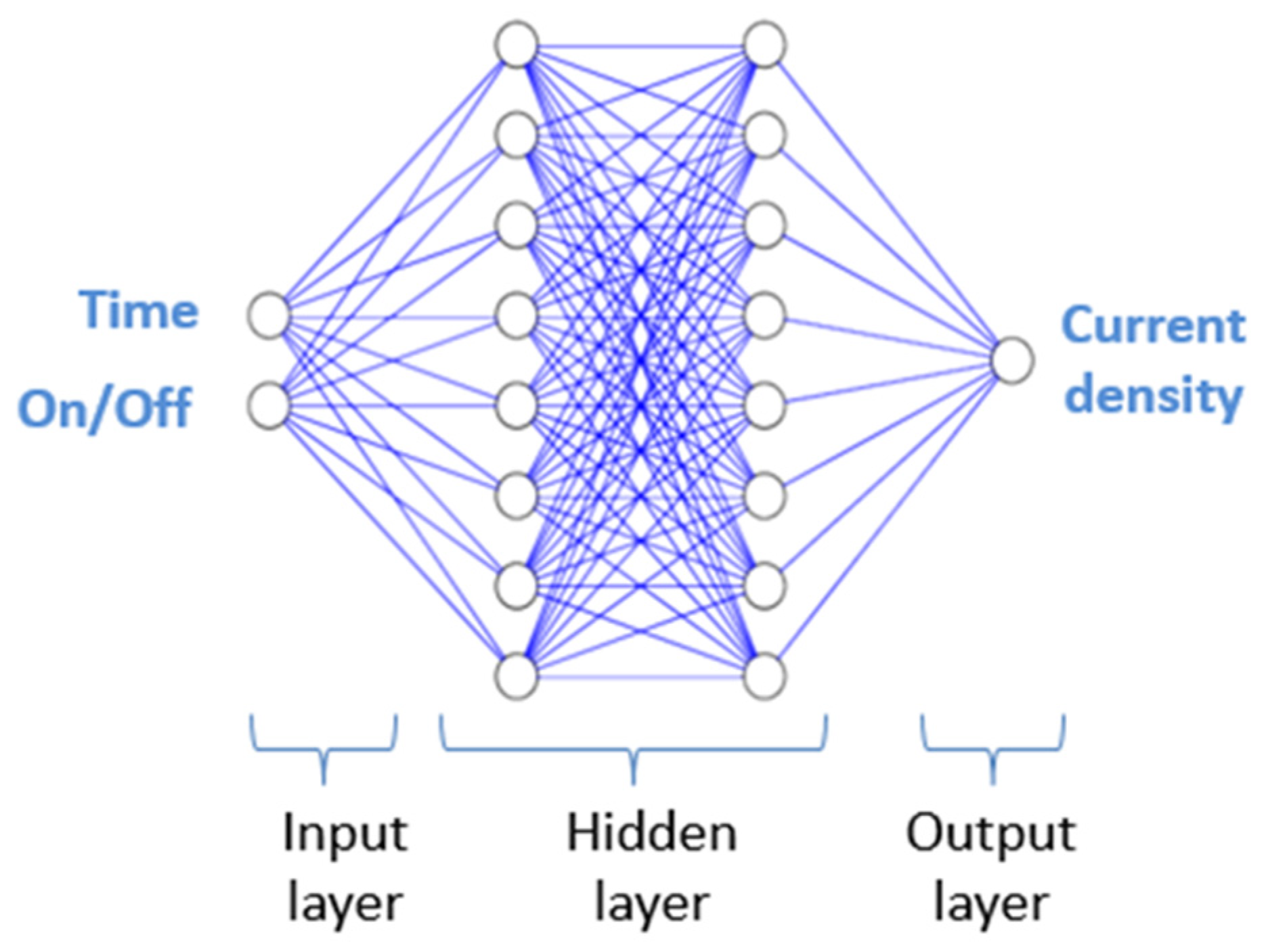
2.3. Artificial Neural Network (ANN) Model Development

ANNs are defined as computing tools that are useful for imitating the learning skills of biological cells and the human brain [15]. In the present study, MATLAB R2018a was used to develop the ANN models. The model parameters are described in Table 1.
The feed-forward neural network with the backpropagation method was used for our model. In this study, two different ANN algorithms were used for training the network: Levenberg–Marquardt (LMANN) and the scaled conjugate gradient (SCGANN). The input layer comprises two numbers of neurons: time and excitation lamp, expressed by “0” for “off” and “1” for “on”, respectively; the ouput layer comprises one (01) neuron photocurrent response, as shown in Figure 2. Out of the 297 runs that were performed, 70% of the data was used for the training of the network. The remaining data was divided as 15% for validation and 15% for the testing of the network, respectively. The collection of the total number of neurons present in the unseen row was performing by observing the mean square error (MSE). The prediction error is defined as the difference between the experimental current density Iexp and that of the model IANN, as shown in Equation (1):
e k = I e x p k I A N N ( k )
where k is the sample number.
The prediction performance of the ANN was evaluated using the coefficient of determination correlation (R), and the mean square error (MSE), as expressed by Equations (2) and (3), respectively:
R = k = 1 N I e x p k I e x p ¯ k = 1 N I A N N k I A N N ¯ k = 1 N I e x p k I e x p ¯ 2 k = 1 N I A N N k I A N N ¯ 2
M S E = 1 N k = 1 N e 2 k
where N is the number of data samples, and I e x p ¯ and I A N N are the mean values of the experimental and predicted values, respectively.

3. Results and Discussion

3.1. Electrochemical Study of WO3 Thin Films

Generally, cyclic voltammetry (CV) is an effective electroanalytical tool for finding redox couples and confirming the electrode potential during the deposition process [29]. The growth of the film either takes place through the condensation of the material or with the adsorption of the colloidal particles from the solution onto the substrate. To better understand the electrochemical behavior during the deposition of tungsten in acidic aqueous solution baths, a systematic cyclic voltammetry study was undertaken on a stainless steel substrate. Figure 3 illustrates typical cyclic voltammograms that were performed at 20 mV s−1 of the working electrode (SS) immersed in the solution containing the tungsten ions at a concentration of 25 mM H2O2, as described in the previous section.
The voltammetry scan was initiated at −0.6 V towards the positive direction of up to 0.8 V vs. Ag/AgCl. From the above graph, it is possible to determine the range of potential and the intensity of current for which the electrodeposition of tungsten is possible. Figure 3 shows the appearance of a first reduction peak (c1) at a potential of about 0.025 V vs. Ag/AgCl, corresponding to the reduction of dissolved oxygen in the solution. The reduction peak observed at −0.3 V (c2) and the pseudo plateau observed at about −0.45 V vs. Ag/AgCl may have been produced due to the reduction in the concentration of species present in the solution. The electrodeposition method is based on the cathodic reduction of a peroxo precursor, obtained by mixing a tungsten precursor with an excess of hydrogen peroxide. This precursor has been described as a dimer with the formula W2O112−, in which the oxidation state of W is (+VI) and O2 denotes a peroxide ligand, respectively [30].
According to Reyes-Gil et al. [28], the mechanism of the deposition of the WO3 is described by Equation (4) [30]:
W2O112− + (2 + x) H+(aq) + x e → 2 WO3(s) + (8 − x)/4 O2(g) + (2 + x)/2 H2O
It has been previously shown that parallel parasitic reactions take place and should correspond to the reduction of free H2O2 and polytungstate [31]. Based on the above electrochemical study, the deposition route of WO3 onto the SS substrate is possible in the potential range between −0.3 and −0.5 vs. Ag/AgCl, respectively. Using XRD analysis, it has been found that the best crystallinity and the well-adherent WO3 thin films were obtained at an optimized deposition potential of −0.45 V (vs. Ag/AgCl).

3.2. Morphological Analysis

3.2.1. Thickness Measurement

The thickness of the WO3 film was measured for each sample using a Dektakt profilometer. The measurements started over the naked substrate part and moved onto the oxide film’s part. The sudden change in the height provided the thickness of the oxide layer. The estimated thicknesses and roughness are listed in Table 2.
It is clear that the thickness of the film increased proportionally with the growth time. The estimated value was found to be 527, 730, and 3277 nm for the samples grown at 10, 15, and 30 min, respectively. For the sample grown at 5 min, it was not possible to measure the thickness of the layer, despite the layer having been well observed with the naked eye; it was therefore expected to be less than 80 nm (cf. Figure 1). In addition, the surface roughness of the WO3 thin oxide also increased with the deposition time, indicating that the films are porous. This behavior is typically obtained for many materials grown using the electrodeposition technique [32,33]. In fact, previous reports have demonstrated that the morphology of the electrodeposited metal oxides depends greatly on the deposition time of the sample [32,34,35,36].

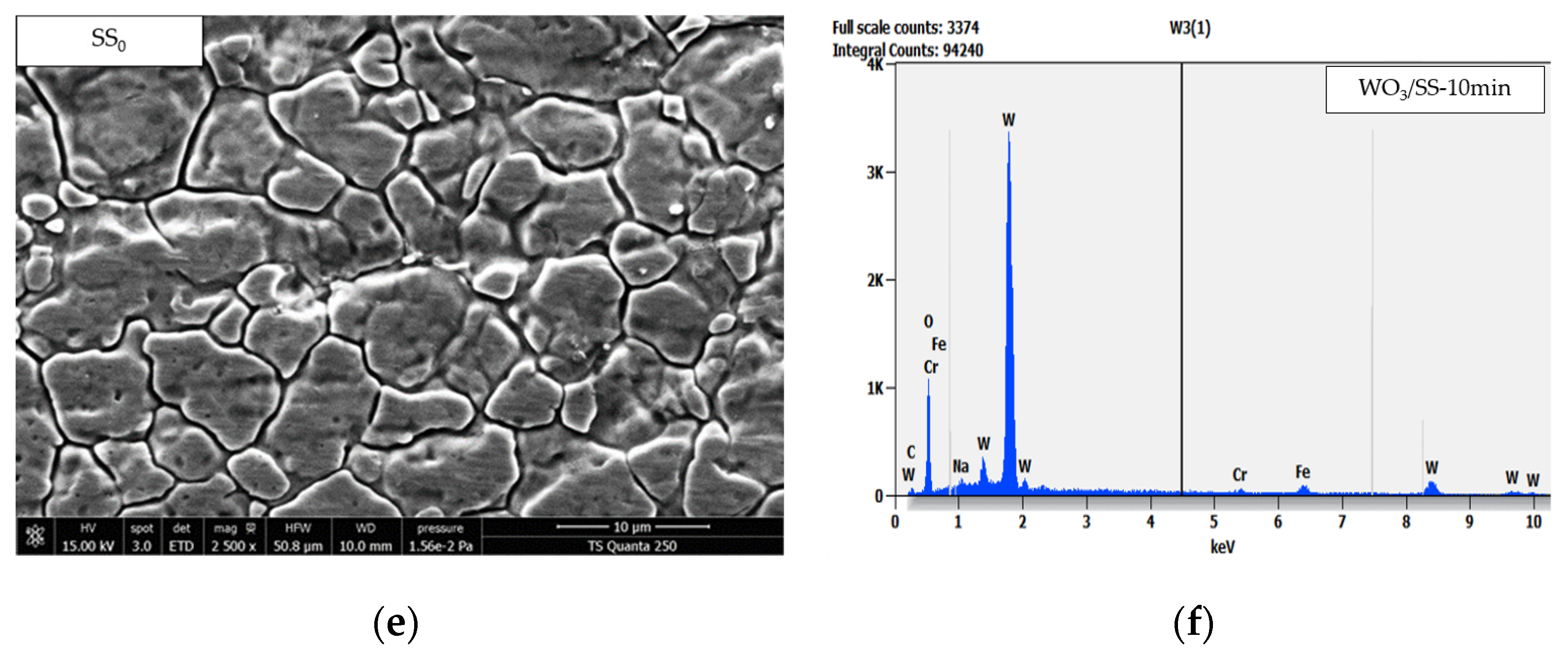
3.2.2. Microscopic Surface Assessment
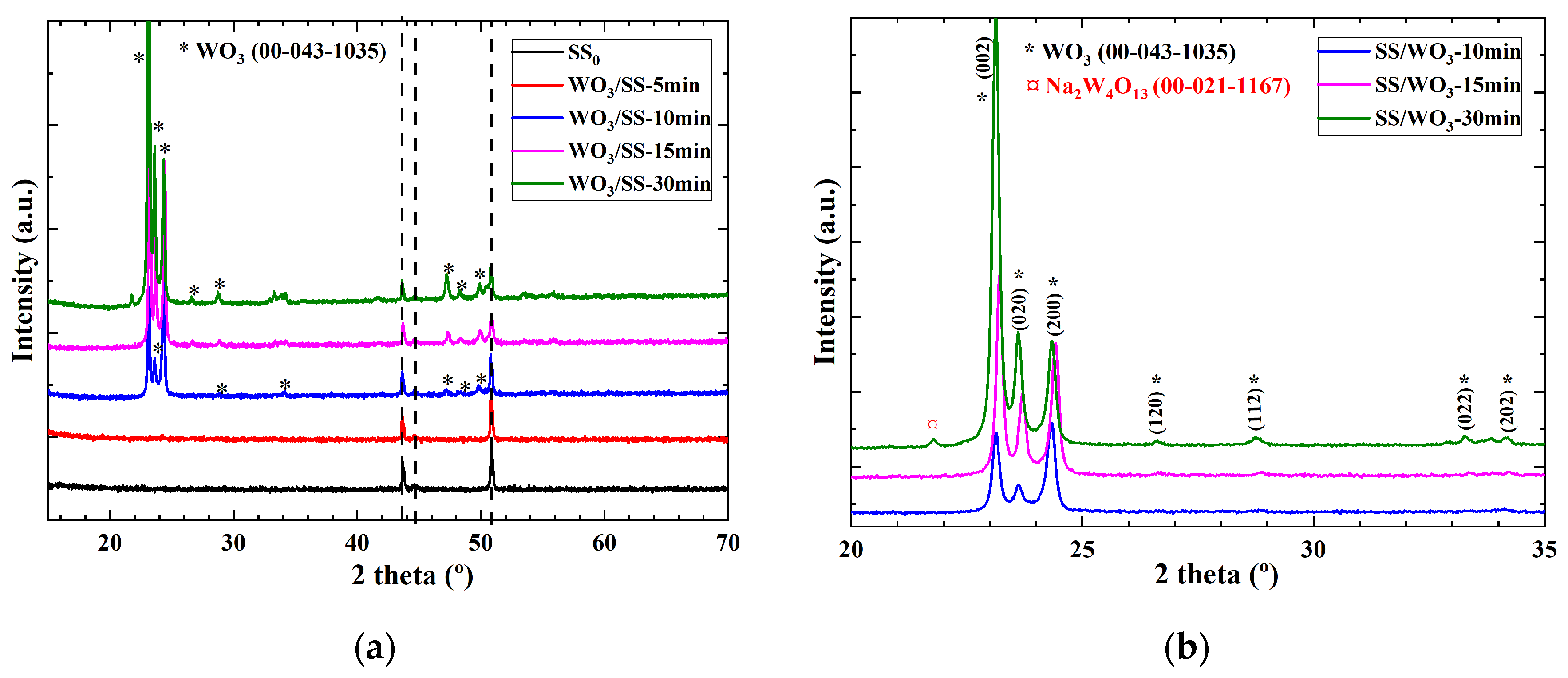
The microstructure of the electrodeposited WO3 thin film onto the stainless steel substrate and their external surface morphology were investigated using scanning electron microscopy (SEM) with a magnification of 2500× (10 µm) and a high magnification of 25,000× (1 µm) (as shown in the insert figure). Figure 4 displays the SEM images of WO3 obtained under different deposition times starting from 5 to 30 min, respectively. As shown in Figure 4a–d and compared to the bare substrate (Figure 4e), all the synthesized samples exhibit different particle shapes and sizes. At a low deposition time (5 min) (Figure 4a) and low thickness, the film displays a rough organization with some holes on the surface. Non-uniform grain sizes and a non-homogenous surface with smaller crystallites (<50 nm) were also obtained. This behavior indicates the amorphous state of WO3 thin films at the initial stage of growth. The low density of these agglomerated crystallites implies that the nucleation has only occurred on a few specific sites. This explains the fact of not being able to measure the thickness with a profilometer. At deposition times equal to 10 min (Figure 4b) and 15 min (Figure 4c), the SEM images reveal a uniform distribution; the stainless steel surface becomes covered with a coalescence of the neighboring crystallites to form relatively large aggregates with a 3D structure. The particle size ranges between ca. 50–100 nm. However, films deposited at higher deposition times of up to 15 min (Figure 4d) show non-uniformed surfaces distinguished by rounded clusters that can be interpreted as crystallized zones limited by grain joints. Similar results have also been reported by Mineo et al., who synthesized nanostructured WO3 onto an ITO substrate using electrodeposition [37]. It can be seen from these SEM images that WO3 samples prepared under different deposition times (or thicknesses) display different morphologies and structural characteristics, which may influence the material’s electrochemical performance as a result. Such variation may come from the continuous growth that occurs during long-time deposition, resulting in the bulky agglomeration observed in the WO3/SS-30 min sample. EDX spectroscopy was used to analyze the synthesized material. The spectrum in Figure 4f indicates that the elemental compositions were W, O, Fe, Cr, and C in the deposited materials. The presence of the Fe, Cr, and C peaks was determined to be related to the SS substrate [14]. In addition to these substrate elements, the intense peaks attributed to tungsten and oxygen were detected, thereby confirming the successful deposition of WO3.

3.3. XRD Analysis

X-ray diffraction (XRD) is a reliable technique that is typically used to determine the crystal structures and phases of the as-prepared films. Figure 5 shows the XRD patterns recorded for the WO3 thin films grown onto the SS substrate with different deposition times ranging from 5 to 30 min, respectively. For all diagrams, the peaks marked by a dashed line were determined to be due to the contribution of the stainless steel substrate with the card number (00-033-0397).
As shown in Figure 5, when the deposition time was increased, the SS peaks significantly decreased as a result. This is in agreement with the layer thickness increase estimated with the profilometer measurements (Table 2). The film deposited at 5 min only showed the peaks attributed to the substrate. This was deemed to be due to the lower thickness of the film (as demonstrated with the profilometer), resulting in the generated XRD signals being of a low intensity. For the rest of the samples, the diffraction peaks were indexed to the SS substrate and WO3 according to the Joint Committee on Powder Diffraction Standards (JCPDS) database with the card number (00-043-1035). WO3 crystallized following the triclinic phase with space group P21/n (14). This result is consistent with data from Reyes-Gil et al. [28], who synthesized WO3 via the electrodeposition technique using the cyclic voltammetry process onto TiO2 nanotubes. It can be noticed that the intensity of the WO3 peaks gradually strengthened as the deposition time increased from 10 to 30 min, respectively. Inversely, the intensity of the substrate decreased, which is coherent with the morphological analysis indicating that the substrate is covered by metal oxides. With the deposition time of 10 min (sample WO3/SS-10 min), the films showed (200) as the preferred orientation, which is more intense and sharper, indicating an improvement in the crystallinity of the grown layers. Moreover, when the deposition time was increased, a change in the preferred orientation was observed (from Figure 5b). The layers exhibited (002) as the preferred orientation at 2Ɵ = 23.05°, indicating the crystallization of the WO3 thin films following the monoclinic phase. This change in the orientation was also reported when studying the deposition time parameter on the structural properties of other semiconductors [34,36], where they have explained the structural change through the surface diffusion and the migration of ad-atoms leading to increasing grain growth during the coalescence stage. This mechanism is coherent with the morphology observation. At the initial stage, when deposition time was low (5 min), an insufficient number of nuclei on the substrates were detected, leading to the absence of the WO3 peaks in the XRD patterns (Figure 5b). When the deposition time was increased to 10 min, a constant nucleation rate appeared, and several nuclei formations during the reaction period were obtained. However, with a deposition time equal to 30 min, a few aggregates were also formed.
In order to determine the preferential orientation of the crystals in the polycrystalline material and to obtain more detailed information regarding the best crystallinity, the crystallite size (D) of the WO3 through the (002) orientation was calculated using the Debye–Scherrer equation (Equation (5)) [38]
D = (0.9 λ)/(β cos θ),
where D is the crystallite size, k is the shape factor (0.9), λ is the wavelength of the incident X-ray from the XRD (λ = 1.5406 Å), β is the observed angular width at a half maximum intensity (FWHM) of the (002) peak, and θ is the Bragg angle of the diffraction peak.
The dislocation density (δ) is typically associated with defaults in the thin films. It represents the number of defects in a crystal. Williamson and Smallman’s equation provides the dislocation density of thin films (Equation (6)) [38]:
δ = 1 D 2
The microstrain (ε) is another interesting structural parameter of WO3 deposited at various times and can be calculated from the following equation:
ε = (βcos θ)/4
As shown in Table 2, the average crystallite size of WO3 films accordingly increased from 4.8 nm to 42 nm with the increase in the deposition time (td) from 10 to 30 min, respectively. This behavior can be explained by the improvement of the monoclinic structure of WO3. Contrary to this latter parameter, the dislocation density decreased from 4.33 × 10⁻¹² m−2 to 5.67 × 10⁻¹⁵ m−2 when the deposition time (td) was increased from 5 to 30 min, respectively.
Comparing these findings with the literature, it was found that the modification in the crystal structure strongly influenced the defects states (bulk and the surface) and the band gap of WO3. Among various crystal structures, the monoclinic structure is highly stable and has been found to be more efficient in water splitting applications [8]. In addition, the crystal structure affects the PEC water splitting activity of WO3. In this context, Kwong et al. [39] prepared WO3 films via electrodeposition using aqueous solutions of peroxotungstic acid with concentrations of 0.05–0.20 mol dm−3. These authors subsequently demonstrated a preferred orientation in monoclinic WO3, which indicates that differential growth rates are dependent upon the tungsten concentration and deposition time. Similarly, Habazaki et al. [40] electrodeposited WO3 film onto an IrO2-coated Ti substrate. These authors demonstrated a transformation of the WO3 crystal phase when increasing the annealing temperature. Additionally, Kwong et al. synthesized WO3 via the electrodeposition method. Their films comprised monoclinic WO3, which exhibited an increased crystallinity with increasing thickness due to a reduced physical mismatch stress [41].

3.4. Optical Properties

The absorption coefficient α and the optical band gap Eg are the most relevant properties for semiconductor thin films. The effect of the deposition time on the optical properties, including the absorption coefficient and energy band gap, has been examined in this study in detail. The experimental values of these two properties were deduced from UV–visible diffuse reflectance spectra in the wavelength range of 200–1100 nm. The variation of the experimental results of the electrodeposited WO3 thin films has been gathered in Figure 6. All the samples showed a high absorption in the visible region, corresponding to the excitonic band gap of the WO3 materials [11]. In addition, the reflectance of all the films were low. This low reflectance value makes the WO3 films an important material for anti-reflection coating [42]. The samples produced at −0.45 V vs. Ag/AgCl for 5, 10, and 15 min exhibited fringes resulting from interfering multiple reflections. The presence of the interference maxima and minima over the spectral region, in which oscillations were observed, indicates that the films are uniform with a smooth surface [43]. The sample deposited at 10 min has a greater number of fringes on the reflectance spectrum. However, when the time went beyond 10 min (WO3/SS-15 min and 30 min), the surface became rough and scattered; such an effect involves the disappearance of the interference phenomena. These findings are in agreement with the morphological study in which it was demonstrated that the increase in the deposition time is accompanied with the formation of aggregates and an inhomogeneous film. The UV–visible diffuse reflectance spectra also showed a red shift of the absorption edge, which reduces the band gap as a result.
To confirm this explanation, the absorption was calculated using the Kubelka–Münk function [14]. This function is induced by Equation (8):
F(R) = (1 − R)2/2R,
where R is the diffuse reflectance.
The optical band gap energy of the samples was measured based on Equation (9) [14]:
αhν = A(hν − Eg)n,
where A is a constant, α is the absorption coefficient, Eg(eV) is the band gap energy of the semiconductor, h is Planck’s constant, ν is the frequency of the incident light, and n is a number that characterizes the type of the transition; as WO3 is a direct-allowed transition material, n = ½.
Therefore, the band gap energy of different WO3 thin films was deduced through extrapolating the linear part of the plots (αhν)2 vs. hν, as grouped in Table 1. The value of the direct band energy represents a gradual decrease from 1.78, 1.68, to 1.36 eV when the deposition time was increased from 10 to 30 min, respectively. The reason behind this energy band gap decrease with the increasing thickness could be attributed to an increase in the particle size and the change in strain, which was previously proven by the XRD results. A decrease in Eg with an increase in the thickness has also been confirmed in other reports [32,34,36]. Comparing these results with previous studies, one can note a relatively low gap energy value. This behavior can be linked to the SS substrate, which provides a good alignment of the metal oxides on its surface. Kwong et al. electrochemically synthesized WO3 on a FTO substrate and obtained an energy gap of 2.50 eV [41]. Additionally, Zhang et al. found an energy value of 2.75 eV for a WO3 nanoflake array synthesized via dealloying an electrodeposited Fe–W amorphous alloy [44].

3.5. Electrochemical Performance

3.5.1. Electrochemical Impedance Spectroscopy (EIS)

EIS is a technique used to investigate the interface between the electrodes and electrolytes [32]. Typically, a small sinusoidal variation is applied to the potential at the working electrode, and the resulting current is analyzed in the frequency domain. The real and imaginary components of the impedance provide information about the kinetic and mass transport properties of the cell, as well as the surface properties through the double-layer capacitance (interface electrolyte/electrode) [32]. The results of this analysis are usually represented in the form of a Nyquist diagram, which represents the evolution of the opposite of the imaginary part of the complex impedance as a function of the real part of the complex impedance over a frequency range (as shown in Figure 7). The obtained data should then be fitted and treated with an equivalent circuit. In this study, the major parameter derived from the EIS curve is the charge transfer resistance at the electrode/electrolyte interface. It provides information on the evolution of the charge carrier mobility following a change in the deposition time.
In this study, the measurements were performed in a three-electrode cell connected to Solartron© Potentiostat using ZPlot© software (ZView© 4.0). Nyquist plots of EIS for the SS substrate and WO3/SS electrode obtained at varied deposition times in the frequency interval from 0.1 Hz to 105 Hz, respectively, are grouped in Figure 7a. As can be noted in Figure 7a, the Nyquist plot of all the WO3/SS electrodes is similar to that of the blank substrate (SS), which was simulated to semicircle curves in the high and medium frequency regions. Considering the EIS spectra, it became possible to model the interface junction using a Randles equivalent circuit simulation using the ZView 4.0. A good match between the experimental and simulated data was observed. This circuit includes an ohmic resistance of the electrolyte solution (Rs), a constant phase element (CPE), which is mainly used to explain the system heterogeneity and distribution of physical properties of the system software, and a charge transfer resistance (Rct) (Figure 7c). The intercept of the semicircle to the real axis (Z′) at a high frequency represents the electrolyte resistance (Rs). Under a low frequency, the intersection at the real axis (Z′) corresponds to the Rs and the Rct. Additionally, the diameter of the semicircles can provide further information regarding the charge transfer resistance of the sample. Conventionally, the diameter of the semicircle in the Nyquist plots represents the electron transfer resistance of the layer and can be used to describe the interface properties of the electrode. In other words, a smaller arc radius means a smaller Rct [14].
Furthermore, one can observe a reduction in the diameter of the semicircle with the increase in the deposition time (or thickness films). This decrease could be attributed to the decreased Rct, significantly improving the interfacial charge transfer and lowering the reaction resistance. As can be deduced from Table 3, the Rs remained constant for all samples with a value ranging between 4.61 Ω and 2.13 Ω, respectively, due to using the same electrolyte solution (1 M NaOH). When the substrate was covered with the WO3 thin films, a reduction in the Rct from 6.12 × 10³ KΩ to 101.15 KΩ, and, inversely, an increase in the constant phase element (CPE) in the range from 86.90 µF to 980.46 µF were observed when the deposition time was increased from 5 to 10 min, respectively. This effect can be explained by the rapid transfer of charge from the WO3 electrode and by the strong accumulation of electrons at the interface as the deposition time increases. This behavior could also be associated with an increase in the grain size and a decrease in the grain boundaries, which is compatible with the results of XRD showing an improvement in the extent of crystallinity following the deposition time. However, Table 3 shows that once the WO3 deposition time was prolonged to 15 and 30 min, the WO3 layer became thicker, and a few aggregates were formed (as observed in the SEM images). This results in a reduction in the CPE values and, inversely, an increase in Rct. A comparison reveals that the sample deposited at 10 min presents lower values of Rct (101.15 KΩ), indicating a reduction in electron recombination and an enhancement in electron transport efficiency.
Moreover, this sample exhibits a higher conductivity related to the capacitance of the CPE of about 980.46 µF. Consequently, WO3 deposited at 10 min exhibits the lowest resistance and the highest double-layer capacitance. Such an effect could be explained by the rapid transfer charge in the WO3/SS electrode and the high electron accumulation at the electrode/electrolyte interface when the deposition time is fixed at 10 min.
When the deposition time was increased to 30 min, there is an increase in Rct and, inversely, a decrease in the CPE, which proves that for this sample, the electronic transfer at the electrode/electrolyte interface is reduced due to the increase in the film’s thickness. The effect of the deposition time or film thickness on the electronic transfer at the electrode was previously studied; researchers have demonstrated that these parameters affect the separation of the e/h+ carriers and enlarge the spectrum response to visible light [45,46].
To elucidate these results, Figure 7b denotes the representative Bode (phase angle vs. frequency) diagrams of the WO3/SS electrodes obtained with different deposition times of WO3. One can observe a phase angle peak at the 0.01–1000 Hz frequency range, indicating a capacitive behavior in the corresponding range for all the samples. Comparing the magnitude value of the phase angle, one can remark that the sample deposited at 10 min (WO3/SS-10 min) depicts the highest value (83.40°). This result suggests that the sample prepared in 10 min exhibits an easy transfer of the charge carriers. This behavior is in agreement with the previously recorded good crystalline quality and appropriate morphology. The peak frequency at the phase angle (fpeak) from the bode phase plots was used to calculate the electron lifetime (τe) using the equation τe = [1/(2π fpeak)] [45]; the values are tabulated in Table 3. Figure 7b also reveals a shift towards the low frequency region when the deposition time was increased from 5 to 30 min, respectively, which increases the values of τe as a result. This shift was determined to be due to the high mobility of the charge carriers, thus reflecting a decrease in the charge transfer resistance and, consequently, an improvement in the flow of electrons through the electrolyte/semiconductor interface [47]. The maximum value for τe was recorded for the 10 min-coated WO3/SS electrode, demonstrating the reduced charge recombination. This suggests a higher efficiency for the 10 min-deposited WO3-coated photoanode.

3.5.2. Photoelectrochemical Study

The PEC measurements also explored the effect of the deposition time on the WO3 thin films. The experiments were conducted under front illumination (WO3/SS thin films side illumination). The cells were irradiated under AM 1.5, simulating the sunlight at 100 mW cm−2, and 0.5 M Na2SO4 was used as an electrolyte solution.
Figure 8 shows the typical characteristics of the current density response to on–off cycling with a total test duration of 300 s. The chronoamperometry (current density–time) curves of the WO3 thin films with the deposition time varied from 5 to 30 min were obtained at a given potential of 0.5 V vs. the Ag/AgCl electrode.
As shown in Figure 8, all the photoanodes produced an instantaneous change (up and down) in the current under on/off illumination switching. This phenomenon proves that the electron/hole pairs were immediately generated and then separated in the metal oxide material. Comparing the samples to each other, it was observed that the photocurrent density increased as the deposition time was increased from 5 to 10 min, respectively. The WO3/SS electrode, which displayed the maximum photocurrent density, had a thickness of 0.52 µm and corresponded to 10 min of the deposition time. These reasons may explain the enhanced PEC activity of the sample prepared at 10 min: firstly, preparing the well-formed and well-annealed thin films in the SEM images (Figure 4) without any impurities facilitates the electronic transfer towards the grains. Secondly, structural results have proven that the electrodeposition process provides high-crystalline WO3 films, especially after a medium deposition time equal to 10 min. However, when the deposition time was prolonged to 15 and 30 min, respectively, the WO3 layer became thicker, and several aggregates were formed (as shown in the SEM images). Under this condition, the photocurrent decreased to 0.061 mA cm−2 and 0.024 mA cm−2 for 15 min and 30 min, respectively. This decrease was mainly attributed to the electronic transfer, which becomes difficult at the WO3/SS electrode interface. This behavior was also confirmed by the lifetime value (Table 3), showing that sample WO3/SS-10 min has the maximum value (0.20 ms). The observed optimum photocurrent value could be attributed to matching the majority carrier diffusion length with the film thickness of the WO3/SS electrode. As a result, the WO3/SS-10 min sample absorbs more photons, producing a higher photocurrent for water oxidation. However, the films deposited at higher times (of more than 10 min) have shown a reduction in the photocurrent. This photocurrent variation was determined to be mainly due to the thickness of the thin film electrode. The photogenerated electrons require traveling beyond the electron diffusion length before being collected at the stainless steel substrate. Conversely, the electron transport within fine WO3 (5 min) could be significantly slower.
To better understand this phenomenon, Figure 9 schematizes the electronic transfer at the WO3/SS electrode interface under illumination. This figure shows that the deposition time or film thickness affects the electronic transfer. In fact, from the morphological properties (Figure 4), for lower deposition times (5 and 10 min), the electron transfer at the interface of the stainless steel substrate took place easily, and the recombination of charge was inhibited. However, Figure 9a shows that once the WO3 deposition time was prolonged to 15 min and 30 min, the semiconductor layer became thicker, forming a few aggregates as a consequence. Under this condition, the electrons lose their energies during the course even before reaching the stainless steel substrate. Consequently, the relatively slow electron transport and associated charge recombination may be the key reasons underlying the diminished photocurrent for the electrodes that correspond to long deposition times. The slow and trap dominant charge transport mechanisms within the photoelectrode have already been reported for several metal oxide semiconductor systems [45,46,47,48]. In general, electron–hole separation, electron and hole transportation, and surface reaction are the key features in designing efficient metal oxide photoanodes for PEC water splitting.
Figure 9b schematizes the relevant processes involved in water splitting using a WO3 semiconductor in a neutral Na2SO4 electrolyte. Thus, under visible light irradiation, and when the semiconductor electrode is immersed in an electrolyte solution, electron transfer takes place between the semiconductor and the electrolyte solution. The corresponding reactions are given by Equations (10)–(12):
WO3/SS + hυ → e (CB) + h+ (VB)
2 OH → ½ O2 + H2O + 2e
2 H2O + 2e → H2 + 2OH
One can observe that the photoexcited holes accumulated on the surface of the WO3 semiconductor are consumed in the oxidation reaction (Equation (11)). At the same time, electrons are transferred to the Pt wire counter electrode via the stainless steel substrate and the external circuit and were used in the water reduction reaction shown in Equation (12). From this study, it is worth noting that the deposition time or the thickness of the WO3 thin films is an effective means to facilitate electron transfer via the electrode/electrolyte interface, thus improving photoelectrochemical activity for water splitting.
In light of these points, WO3 photoanodes of various morphologies have been synthesized, including nanoflakes, nanoplates, nanosheets, nanorods, and nanowires. It has been demonstrated that these parameters clearly affect the photocurrent density value [8].
The photocurrent of the WO3/SS photoelectrode obtained in this study has been compared to other electrodes studied in earlier reports (as detailed in Table 4). It can be found that many parameters affect the PEC response of the photoelectrode. Indeed, Kwong et al. studied the effect of the applied potential on the PEC properties of their WO3 photoanode electrodeposited onto a FTO substrate [41]. They demonstrated that a higher photocurrent density was obtained for the films synthesized at a cathodic potential of −0.5 V vs. Ag/AgCl, leading to a photocurrent value of about 28 µA cm−2 at 0.7 V vs. Ag/AgCl [41]. Photo-corrosion-resistant WO3 nanoflake arrays were synthesized via a new route involving dealloying an electrodeposited Fe–W amorphous alloy and subsequent thermal treatment in air. The obtained photocurrent was about 2.25 mA cm−2 at a bias potential of 1.5 V (vs. SCE) [44]. Fan et al. [49] and Kalanur et al. [50] proved that the 1D nanostructure-based WO3 photoanode has a higher interfacial contact area than bulk WO3. According to Kalanur et al. [8], nanostructured WO3 synthesized using hydrothermal and doctor blade methods exhibited the highest photocurrent compared to the WO3 obtained using the electrodeposition technique. Zhu et al. [51] obtained a typical photocurrent density value of 35 µA cm−2 at a bias of 1 V vs. Ag/AgCl for the WO3/FTO photoanode elaborated via electrodeposition and annealed at 600 °C. Recently, Suspanantin et al. demonstrated that the fabricated WO3 electrode ameliorated photoelectrochemical water oxidation when using the amperometric method or the cyclic voltammetric method than when using the traditional spin coating method, up to four times and sixty times, respectively. The optimum value obtained was about 120 µA [52]. In fact, when comparing the present results to those published earlier (Table 4), it can be seen that obtained value from this study is two times higher. This finding confirms the beneficial effect of stainless steel substrates compared to those that are typically used (e.g., FTO, ITO, and SnO2).

3.6. ANN Modeling of the Photocurrent
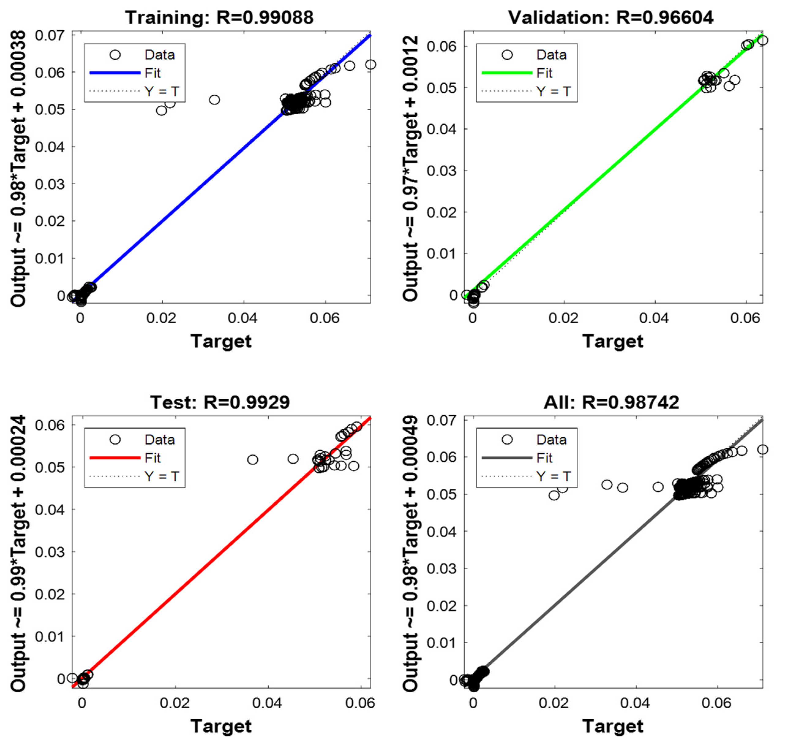
In this study, the ANN model was designed using sigmoid transfer functions. The time and the off/on state of the excitation lamp (expressed by “0” for “off” and “1” for “On”, respectively) were both selected as the input variables, while the current density response was selected as the output variable, respectively. A total of 297 experimental datasets from preliminary studies were used to feed the ANN structure. These datasets were divided into 70%: training, 15%: validation, and 15%: testing, respectively. The hidden layer was formed using a number of neurons that can be varied to optimize the performance of the intelligent model (Figure 2).
One of the major problems facing researchers is the selection of hidden neurons using these neural networks. This is important while the neural network is being trained to obtain minimal errors that may not respond properly in terms of renewable energy prediction.
In this study, the number of hidden neurons varied from five to thirty-five during training, respectively, which allowed us to choose the best value corresponding to the best network performance. As previously announced in the experimental section, two ANN algorithms were used for training: Levenberg–Marquardt (LMANN) and the scaled conjugate gradient (SCGANN). The evaluation of the neural network performance was based on two parameters: the mean square error (MSE) and the correlation coefficient (R), which were calculated following Equations (2) and (3), respectively (see experimental section).

3.6.1. LMANN

The Levenberg–Marquardt algorithm is typically used to provide a solution to complicated problems, which are often non-linear and dependent on several variables. The mean square error (MSE) is calculated as the average of the squared differences between the predicted and experimental outputs. The correlation coefficient is defined as the process of fitting the models to the data.
Table 5 summarizes the values of the MSE and R obtained for the training, validation, and testing performances using the LMANNs as ANN algorithms. Generally, a small MSE and a large R value indicate good prediction results. As shown in Table 5, the best performance corresponded to fifteen hidden neurons in which the MSE of training had the smallest value, and conversely, the correlation coefficient R was close to one.
To elucidate this behavior, Figure S1 in the Supplementary Information (SI) represents the results of the photoanode, which found approximately 15 hidden neurons. In fact, the ‘15’ hidden neurons value gave the most effective result of the WO3 thin film as a photoanode. As a result, according to Table 5 and Figure S1, the obtained R values for the training, validation, and testing datasets imply a strong reliability of the models that were used. With 15 hidden neurons, the architecture 2-15-1 corresponds to: two inputs, fifteen hidden neurons, and one output, respectively, which together can be used to predict the photocurrent in the WO3 photoanode electrode. Accordingly, the optimal number of neurons in the input, hidden, and output layers, namely two, fifteen, and one, respectively, was selected as the optimum topography to model the WO3 PEC process. The set of connection weights and biases that cause the optimum ANN topography are listed in Table 6.
A regression analysis of the 2-15-1 LMANN network response between the output and the corresponding target was performed. The regression plots of the trained network are shown in Figure 10. The overall regression coefficient obtained was 0.98742, with the regression coefficients for the training, validation, and testing of all data sets being 0.99088, 0.96604, and 0.9929, respectively. These values confirm that this ANN model was trained successfully and is ready to simulate the outputs from a given set of inputs.

3.6.2. SCGANN

The second ANN algorithm used for training was the scaled conjugate gradient (SCGANN). This algorithm is based on conjugate directions, such as in traincgp, traincgf, and traincgb, but this algorithm does not perform a line search at each iteration. It is one of the most effective standard backpropagation algorithms. Table 7 presents the training, validation, and testing performance of the SCGANN. One can note from Table 7 and Figure S2 in SI that the best performance parameters were found to correspond to five hidden neurons for which the lower value of the validation MSE was obtained. Therefore, in this case, the best topography of the SCGANN model to predict the photocurrent was determined as 2-5-1. The corresponding weights and biases are listed in Table 8.
The developed SCGANN model was assessed for its validity by comparing the model-predicted values of the decolorization efficiency of the test set with those obtained from the corresponding experiments. A comparison between these values has been displayed in Figure 11. The obtained correlation coefficient (R) of the line indicates the excellent performance of this ANN model in predicting the experimental data.

3.6.3. Comparative Study

In this study, two types of algorithms, including the LMANN and the SCGANN, were investigated. The comparative study (illustrated in Figure 12) revealed that both the LMANN and SCGANN models are able to significantly predict and optimize the photocurrent of the WO3 thin films electrode, evidenced by the training correlation coefficient (R) values of 0.9908 and 0.993, respectively, which indicates that the observed and predicted values are strongly correlated. As can be seen, there is a good agreement between the measured data (blue curve) and the model fit (red curve). These performance results show that both developed ANN models were accurate.
However, when comparing the two programs with each other, one can clearly see that the LMANN algorithm provides a better resolution to the photocurrent response of the WO3/SS photoelectrode with a validation correlation coefficient (R) of 0.96604 and an error of 0.004% compared to the SCGANN, which gave an error of 0.124%. This finding explains why the LMANN was more susceptible to over-fitting and yielded an inferior prediction ability than the SCGANN.

4. Conclusions

The present work assessed the performance of WO3 thin films as photoanodes electrodeposited onto a SS substrate for PEC water splitting. Through employing the electrodeposition technique, the deposition time was tailored to optimize the WO3 thin films surface coating over the SS substrate. The influence of this parameter (in other words, the film thickness) on the morphological, structural, optical, and electrical properties has been discussed in detail and was correlated with the PEC performance. The highest photocurrent density was obtained for the WO3 thin film elaborated at 10 min (WO3/SS-10 min). The improved PEC response was attributed to the increased visible light absorption and the efficient separation of the photogenerated carriers at the electrode/electrolyte interface with the optimum time of 10 min. This behavior was attributed to the good crystallinity and homogeneous distribution of the WO3 nanoparticles onto the substrate surface with a deposition time optimized to 10 min.
In the second part, the characteristics of the WO3 thin film obtained at 10 min as a photoanode were successfully simulated using an ANN. Moreover, there was a high agreement between the experimental and ANN modeling values, which was confirmed with the low error percentage, low MSE (ca. 0), and the regression factor R (ca. 1). These results showed that the lower number of secret neurons engineering indicates the best execution in regard to the MSE and the correlation coefficient of the relationship. Different average errors of the WO3 thin film as a photoanode for water splitting were found for different neuron values.
These performance results show that the developed ANN model is accurate. As a conclusion of this study, it can be deduced that the proposed intelligent model is suitable for predicting the PEC response behavior.
To increase the PEC efficiency of this photoanode, the next appropriate step would to move from a thin layer to a nanostructure. The challenge will be to deposit the optimized synthesized WO3 electrode onto an anodized stainless steel substrate. As an electrode for renewable energy applications (hydrogen production or energy storage), this 2D-arrayed nanostructure will exhibit superior electrical properties, such as a significantly large areal capacitance, tight binding with current collectors, and retarded saturation of the capacitance, compared to a planar WO3 thin films electrode.
Future work will focus on the electrochemical performance of the nanostructured WO3/anodized stainless steel substrate, while attempting to adapt the developed ANN model used in the present work to predict other electrochemical and electrical parameters of the photoanode.

Supplementary Materials

The following supporting information can be downloaded at: https://www.mdpi.com/article/10.3390/su151511751/s1, Figure S1: Performance of the LMANN model as a function of the MSE during training, validation, and testing; Figure S2: Performance of the SCGANN model as a function of the MSE during training, validation, and testing.

Author Contributions

Conceptualization M.D., A.A. and I.B.A.; methodology, A.A., M.D. and I.B.A.; investigation, A.B., A.A. and R.C.; writing—original draft preparation, M.D. and A.A.; writing—review and editing, I.B.A., D.M.F.S. and A.B.; visualization, R.C. and D.M.F.S.; resources, R.C.; supervision, I.B.A. and R.C. All authors have read and agreed to the published version of the manuscript.

Funding

The authors would like to acknowledge the financial support of the Tunisian Ministry of higher education and scientific research as well as the University of Sfax and from the PEJC19PEJC04-01 project (Programme d’Encouragement des Jeunes Chercheurs PEJC, 2ème Edition (2018), Tunisia). Fundação para a Ciência e a Tecnologia (FCT, Portugal) has been acknowledged for funding a research contract in the scope of programmatic funding UIDP/04540/2020 (D.M.F. Santos).

Data Availability Statement

The authors confirm that all relevant data generated during this study are included in this published article.

Conflicts of Interest

The authors declare no conflict of interest. The funders had no role in the design of the study; in the collection, analyses, or interpretation of data; in the writing of the manuscript; or in the decision to publish the results.

References

  1. Fujishima, A.; Honda, K. Electrochemical photolysis of water at a semiconductor electrode. Nature 1972, 238, 37–38. [Google Scholar] [CrossRef]
  2. Josny, J.; Jinu, M.; Soney, C.G. Nanomaterials for photoelectrochemical water splitting review. Int. J. Hydrogen Energy 2018, 43, 4804–4817. [Google Scholar]
  3. Eidsvag, H.; Bentouba, S.; Vajeeston, P.; Yohi, S.; Velauthapillai, D. TiO2 as a photocatalyst for water splitting-an experimental and theoretical review. Molecules 2021, 26, 1687. [Google Scholar] [CrossRef]
  4. Ma, M.; Huang, Y.; Liu, J.; Liu, K.; Wang, Z.; Zhao, C.; Qu, S.; Wang, Z. Engineering the photoelectrochemical behaviors of ZnO for efficient solar water splitting. J. Semicond. 2020, 41, 091702. [Google Scholar] [CrossRef]
  5. Najaf, Z.; Nguyen, D.L.T.; Chae, S.Y.; Joo, O.S.; Shah, A.U.H.A.; Vo, D.V.N.; Nguyen, V.H.; Le, Q.V.; Rahman, G. Recent trends in development of hematite (α-Fe2O3) as an efficient photoanode for enhancement of photoelectrochemical hydrogen production by solar water splitting. Int. J. Hydrogen Energy 2021, 46, 23334–23357. [Google Scholar] [CrossRef]
  6. Jian, J.; Xu, Y.; Yang, X.; Liu, W.; Fu, M.; Yu, H.; Xu, F.; Feng, F.; Jia, L.; Friedrich, D.; et al. Embedding laser generated nanocrystals in BiVO4 photoanode for efficient photoelectrochemical water splitting. Nat. Commun. 2019, 10, 2609. [Google Scholar] [CrossRef] [PubMed] [Green Version]
  7. Gondolini, A.; Sangiorgi, N.; Sangiorgi, A.; Sanson, A. Photoelectrochemical Hydrogen Production by Screen-Printed Copper Oxide Electrodes. Energies 2021, 14, 2942. [Google Scholar] [CrossRef]
  8. Kalanur, S.; Duy, L.T.; Seo, H. Recent Progress in Photoelectrochemical Water Splitting Activity of WO3 Photoanodes. Top. Catal. 2018, 61, 1043–1076. [Google Scholar] [CrossRef]
  9. Kalanur, S.S. Structural, Optical, Band Edge and Enhanced Photoelectrochemical Water Splitting Properties of Tin-Doped WO3. Catalysts 2019, 9, 456. [Google Scholar] [CrossRef] [Green Version]
  10. Kalanoor, B.S.; Seo, H.; Kalanur, S.S. Recent developments in photoelectrochemical water-splitting using WO3/BiVO4 heterojunction photoanode: A review. Mater. Sci. Energy Technol. 2018, 1, 49–62. [Google Scholar]
  11. Zhu, T.; Chong, M.N.; Chan, S. Nanostructured Tungsten Trioxide Thin Films Synthesized for Photoelectrocatalytic Water Oxidation: A review. ChemSusChem 2014, 7, 2974–2997. [Google Scholar] [CrossRef] [PubMed]
  12. Shinde, P.S.; Go, G.H.; Lee, W.J. Multilayered large-area WO3 films on sheet and mesh-type stainless steel substrates for photoelectrochemical hydrogen generation. Int. J. Energy Res. 2011, 37, 323–330. [Google Scholar] [CrossRef]
  13. Lamouchi, A.; Ben Assaker, I.; Chtourou, R. Enhanced photoelectrochemical activity of MoS2-decorated ZnO nanowires electrodeposited onto stainless steel mesh for hydrogen production. Appl. Surf. Sci. 2019, 478, 937–945. [Google Scholar] [CrossRef]
  14. Lamouchi, A.; Slimi, B.; Ben Assaker, I.; Gannouni, M.; Chtourou, R. Correlation between SSM substrate effect and physical properties of ZnO nanowires electrodeposited with or without seed layer for enhanced photoelectrochemical applications. Eur. Phy. J. Plus 2016, 131, 201. [Google Scholar] [CrossRef]
  15. Snežana, D. Artificial neural network modeling in environmental radioactivity studies—A review. Sci. Total Environ. 2022, 847, 157526. [Google Scholar]
  16. Ameer, K.; Ameer, S.; Kim, Y.M.; Nadeem, M.; Park, M.K.; Murtaza, M.A.; Khan, M.A.; Nasir, M.A.; Din, G.M.; Mahmood, S.; et al. A Hybrid RSM-ANN-GA Approach on Optimization of Ultrasound-Assisted Extraction Conditions for Bioactive Component-Rich Stevia rebaudiana (Bertoni) Leaves Extract. Foods 2022, 11, 883. [Google Scholar] [CrossRef] [PubMed]
  17. Talwar, S.; Verma, A.K.; Sangal, V.K. Modeling and optimization of fixed mode dual effect (photocatalysis and photo-Fenton) assisted Metronidazole degradation using ANN coupled with genetic algorithm. J. Environ. Manag. 2019, 250, 109428. [Google Scholar] [CrossRef]
  18. Alsaffar, M.A.; Ayodele, B.V.; Mustapa, S.I. Scavenging carbon deposition on alumina supported cobalt catalyst during renewable hydrogen-rich syngas production by methane dry reforming using artificial intelligence modeling technique. J. Clean. Prod. 2020, 247, 119168. [Google Scholar] [CrossRef]
  19. Mousavi, S.A.; Vasseghian, Y.; Bahadori, A. Evaluate the performance of Fenton Process for the Removal of Methylene Blue from Aqueous solution: Experimental, Neural Network Modeling and Optimization. Environ. Prog. Sustain. 2020, 39, 1–7. [Google Scholar] [CrossRef]
  20. Luna, M.D.G.; Sablas, M.M.; Hung, C.M.; Chen, C.W.; Segura, S.G.; Dong, C.D. Modeling and optimization of imidacloprid degradation by catalytic percarbonate oxidation using artificial neural network and Box-Behnken experimental design. Chemosphere 2020, 251, 126254. [Google Scholar] [CrossRef]
  21. Xinyua, L.; Peng, L.; Krishna, B.; Yue, C.; Xuemin, D.; Yangping, W.; Yifu, Z.; Liangmei, R.; Quan, X.; Jingkun, X. An emerging machine learning strategy for electrochemical sensor and supercapacitor using carbonized metal–organic framework. J. Electroanal. Chem. 2022, 920, 116634. [Google Scholar]
  22. Rahimi, M.; Abbaspour-Fard, M.H.; Rohani, A. A multi-data-driven procedure towards a comprehensive understanding of the activated carbon electrodes performance (using for supercapacitor) employing ANN technique. Renew. Energy 2021, 180, 980–992. [Google Scholar] [CrossRef]
  23. Alimi, A.; Ben Assaker, I.; Mozaryn, J.; Avila-Brande, D.; Castilli-Martinez, E.; Chtourou, R. Electrochemical synthesis of MnO2/NiO/ZnO trijunction coated stainless steel substrate as a supercapacitor electrode and cyclic voltammetry behavior modeling using artificial neural network. Int. J. Energy Res. 2022, 46, 17163–17179. [Google Scholar] [CrossRef]
  24. Pascal, F.; Gabriel, D.P.G.; Riccardo, D.B.; Alán, A.G.; David, B. Machine learning dihydrogen activation in the chemical space surrounding Vaska’s complex. Chem. Sci. 2020, 11, 4584–4601. [Google Scholar]
  25. Tao, Q.; Lu, T.; Sheng, Y.; Li, L.; Lu, W.; Li, M. Machine learning aided design of perovskite oxide materials for photocatalytic water splitting. J. Energy Chem. 2021, 60, 351–359. [Google Scholar] [CrossRef]
  26. Oral, B.; Can, E.; Yildirim, R. Analysis of photoelectrochemical water splitting using machine learning. Int. J. Hydrogen Energy 2022, 47, 19633–19654. [Google Scholar] [CrossRef]
  27. Wang, Z.; Gu, Y.; Zheng, L.; Hou, J.; Zheng, H.; Sun, S.; Wang, L. Machine Learning Guided Dopant Selection for Metal Oxide-Based Photoelectrochemical Water Splitting: The Case Study of Fe2O3 and CuO. Adv. Mater. 2022, 34, 2106776. [Google Scholar] [CrossRef] [PubMed]
  28. Reyes-Gil, K.R.; Robinson, D.B. WO3-Enhanced TiO2 Nanotube Photoanodes for Solar Water Splitting with Simultaneous Wastewater Treatment. ACS Appl. Mater. Interfaces. 2013, 5, 12400–12410. [Google Scholar] [CrossRef]
  29. Saidi, H.; Boujmil, M.F.; Bouicha, M. Effect of the electrodeposition potential on the physical properties of rapid thermal processing annealed CuInSe2 films. Phys. Status Solidi A 2023, 220, 2200808. [Google Scholar] [CrossRef]
  30. Pauporté, T. A Simplified method for WO3 electrodeposition. J. Electrochem. Soc. 2002, 149, C545. [Google Scholar] [CrossRef]
  31. Meulenkamp, E.A. Mechanism of WO3 Electrodeposition from Peroxy-Tungstate Solution. J. Electrochem. Soc. 1997, 144, 1664. [Google Scholar] [CrossRef]
  32. Landolsi, Z.; Ben Assaker, I.; Chtourou, R.; Ammar, S. Photoelectrochemical impedance spectroscopy of electrodeposited hematite α-Fe2O3 thin films: Effect of cycle numbers. J. Mater. Sci. Mater. 2018, 29, 81787–88187. [Google Scholar] [CrossRef]
  33. Biswal, A.; Panda, P.K.; Acharya, A.N.; Mohapatra, S.; Swain, N.; Tripathy, B.C.; Jiang, Z.T.; Sundaram, M.M. Role of Additives in Electrochemical Deposition of Ternary Metal Oxide Microspheres for Supercapacitor Applications. ACS Omega 2020, 5, 3405–3417. [Google Scholar] [CrossRef]
  34. Braiek, Z.; Gannouni, M.; Ben Assaker, I.; Bardaoui, A.; Lamouchi, A.; Brayek, A.; Chtourou, R. Correlation between physical properties and growth mechanism of In2S3 thin films fabricated by electrodeposition technique with different deposition times. Eur. Phys. J. Appl. Phys. 2015, 72, 10. [Google Scholar] [CrossRef]
  35. Tamboli, S.H.; Rahman, G.; Joo, O.S. Influence of potential, deposition time and annealing temperature on photoelectrochemical properties of electrodeposited iron oxide thin film. J. Alloys Compd. 2012, 520, 232–237. [Google Scholar] [CrossRef]
  36. Gannouni, M.; Ben Assaker, I.; Chtourou, R. Role of deposition time on structural, optical and electrical properties of In-rich Cu-In-S spinel films grown by electrodeposition technique. Superlattices Microstruct. 2013, 61, 22–32. [Google Scholar] [CrossRef]
  37. Mineo, G.; Ruffino, F.; Mirabella, S.; Bruno, E. Investigation of WO3 electrodeposition leading to nanostructured thin films. J. Nanomater. 2020, 10, 1493. [Google Scholar] [CrossRef]
  38. Warren, B.E. X-ray Diffraction; Dover: New York, NY, USA, 1990; p. 253. [Google Scholar]
  39. Kwong, W.L.; Savvides, N.; Sorrell, C.C. Electrodeposited nanostructured WO3 thin films for photoelectrochemical applications. Electrochem. Acta 2012, 75, 371–380. [Google Scholar] [CrossRef]
  40. Habazaki, H.; Hayashi, Y.; Konno, H. Characterization of electrodeposited WO3 films and its application to electrochemical wastewater treatment. Electrochem. Acta 2002, 47, 4181–4188. [Google Scholar] [CrossRef]
  41. Kwong, W.L.; Qiu, H.; Nakaruk, A.; Koshy, P.; Sorrell, C.C. Photoelectrochemical Properties of WO3 Thin Films Prepared by Electrodeposition. Energy Procedia 2013, 34, 617–626. [Google Scholar] [CrossRef] [Green Version]
  42. Zayim, E.O. Optical and electrochromic properties of sol-gel made anti-reflective WO3-TiO2 films. Sol. Energy Mater Sol. Cells 2005, 87, 695–703. [Google Scholar] [CrossRef]
  43. Bourezgui, A.; Kacem, I.; Ben Assaker, I.; Gannouni, M.; Ben Naceur, J.; Karyaoui, M.; Chtourou, R. Synthesis of porous TiO2 thin films prepared with templating technique to improve the photoelectrochemical properties. J. Porous Mater. 2016, 23, 1085–1094. [Google Scholar] [CrossRef]
  44. Zhang, J.; Ling, Y.; Gao, W.; Wang, S.; Li, J. Enhanced photoelectrochemical water splitting on novel nanoflake WO3 electrodes by dealloying of amorphous Fe-W alloys. J. Mater. Chem. A 2013, 1, 10677–10685. [Google Scholar] [CrossRef]
  45. Wadhene, R.; Lamouchi, A.; Ben Assaker, I.; Ben Naceur, J.; Martínez-Huerta, M.V.; Chtourou, R. Electrodeposition of Cu2ZnSnS4 thin films onto TiO2 nanorods for photocatalytic application: Effect of deposition time. Inorg. Chem. Commun. 2020, 122, 108298. [Google Scholar] [CrossRef]
  46. Braiek, Z.; Ben Assaker, I.; Gannouni, M.; Alem, H.; Roques-Carmes, T.; Chtourou, R. Impact of In2S3 shells thickness on the electrochemical and optical properties of oriented ZnO/In2S3 core/shell nanowires. Int. J. Hydrogen Energy 2017, 42, 5694–5707. [Google Scholar] [CrossRef]
  47. Gannouni, M.; Ben Assaker, I.; Chtourou, R. Experimental investigation of the effect of indium content on the CuIn5S8 electrodes using electrochemical impedance spectroscopy. Mater. Res. Bull. 2014, 61, 519–527. [Google Scholar] [CrossRef]
  48. Ben Naceur, J.; Jrad, F.; Souiwa, F.; Ben Rhouma, F.; Chtourou, R. Hydrothermal reaction time effect in wettability and photoelectrochemical properties of TiO2 nanorods arrays films. Optik 2021, 239, 1666794. [Google Scholar] [CrossRef]
  49. Fan, X.; Gao, B.; Wang, T.; Huang, X.; Gong, H.; Xue, H.; Guo, H.; Song, L.; Xia, W.; He, J. Layered double hydroxide modified WO3 nanorod arrays for enhanced photoelectrochemical water splitting. Appl Catal. A Gen. 2016, 528, 52–58. [Google Scholar] [CrossRef]
  50. Kalanur, S.S.; Hwang, Y.J.; Chae, S.Y.; Joo, O.S. Facile growth of aligned WO3 nanorods on FTO substrate for enhanced photoanodic water oxidation activity. J. Mater. Chem. A 2013, 1, 3479–3488. [Google Scholar] [CrossRef]
  51. Zhu, T.; Chong, M.N.; Phuan, Y.W.; Chan, E.S. Electrochemically synthesized tungsten trioxide nanostructures for photoelectrochemical water splitting: Influence of heat treatment on physicochemical properties, photocurrent densities and electron shuttling. Colloids Surf. A Physicochem. Eng. 2015, 484, 297–303. [Google Scholar] [CrossRef]
  52. Supanantin, F.; Ponchio, C. Improvement ITO/WO3 photo anode electrode fabrication using electrodeposition technique for highly efficient photoelectrocatalytic insecticide degradation. Mater. Sci. Semicond. Process. 2020, 118, 105212. [Google Scholar] [CrossRef]
  53. Hilliard, S.; Baldinozzi, G.; Friedrich, D. Mesoporous thin film WO3 photoanode for photoelectrochemical water splitting: A sol-gel dip coating approach. Sustain. Energy Fuels 2017, 1, 145–153. [Google Scholar] [CrossRef] [Green Version]
  54. Li, L.; Zhao, X.; Pan, D.; Li, G. Nanotube array-like WO3/W photoanode fabricated by electrochemical anodization for photoelectrocatalytic overall water splitting. Chin. J. Catal. 2017, 38, 2132–2140. [Google Scholar] [CrossRef]
  55. Ma, Z.; Hou, H.; Song, K. Engineering oxygen vacancies by one-step growth of distributed homojunctions to enhance charge separation for efficient photoelectrochemical water splitting. Chem. Eng. J. 2020, 379, 122266. [Google Scholar] [CrossRef]
Figure 1. Electrochemical synthesis of the WO3/SS photoanode with different deposition times.
Sustainability 15 11751 g001
Figure 2. Architecture of the ANN.
Sustainability 15 11751 g002
Figure 3. Cyclic voltammogram of SS in an aqueous solution containing 25 mM Na2WO4 + 30 mM H2O2 at a pH of 1.4, run with a scanning rate of 20 mV s−1 at room temperature.
Sustainability 15 11751 g003
Figure 4. SEM images (2500×) of WO3 electrodeposited onto the SS substrate at (a) 5 min, (b) 10 min, (c) 15 min, (d) 30 min, and (e) naked SS substrate, with 25,000× magnification as the inset. (f) EDX spectrum of the WO3/SS-10 min thin film.
Sustainability 15 11751 g004aSustainability 15 11751 g004b
Figure 5. (a) XRD patterns of electrodeposited WO3 with an applied potential of −0.45 V vs. Ag/AgCl onto the SS substrate at different deposition times varied from 5 to 30 min, respectively. (b) enlarged main peaks of WO3 at deposition times of 10, 15, and 30 min, respectively.
Sustainability 15 11751 g005
Figure 6. UV–Vis reflectance spectra of the WO3 films onto the SS substrate deposited at 5, 10, 15, and 30 min, respectively.
Sustainability 15 11751 g006
Figure 7. Electrochemical impedance spectroscopy (EIS) results. Nyquist plots (a), equivalent circuit (b), and Bode plots (c), obtained at an open circuit voltage of WO3 thin films electrodeposited onto the SS substrate at deposition times varied from 5 to 30 min, respectively.
Sustainability 15 11751 g007
Figure 8. Photocurrent response under pulsed illuminations of the WO3/SS photoanodes deposited at different deposition times varied from 5 to 30 min, respectively.
Sustainability 15 11751 g008
Figure 9. (a) Mechanism of growth with different deposition times and (b) schematic illustration of the electronic transfer in the PEC device.
Sustainability 15 11751 g009
Figure 10. Linear regression between the experimental output and the corresponding LMANN target. Y: experimental, and T: predicted.
Sustainability 15 11751 g010
Figure 11. Linear regression between the experimental output and the corresponding SCGANN target. Y: experimental, and T: predicted.
Sustainability 15 11751 g011
Figure 12. Experimental photocurrent and predicted curves using the LMANN (a) and SGANN (b) models.
Sustainability 15 11751 g012
Table 1. Artificial neural network (ANN) model training parameters and structure.
ANN Model ParametersValue/Type
Number of input neurons2
Number of output neurons1
Number of hidden layer neurons5, 10, 15, 20, 25, 30, and 35
The initial weights and biasesNguyen–Widrow initialization
Activation functionSigmoid activation function
Learning ruleLevenberg–Marquardt back propagation algorithm
Scaled conjugate gradient algorithm
Table 2. Evolution of deposited material amount, crystallite size (D), dislocation density (δ), microstrain (ε), optical band gap (Eg), thickness, and roughness with deposition time.
ParametersWO3/SS-5 minWO3/SS-10 minWO3/SS-15 minWO3/SS-30 min
Deposited material (10−3 g)0.15–0.180.44–0.460.54–0.571.33–1.36
Thickness (µm)-0.52–0.550.71–0.733.20–3.26
roughness (μm)-0.18 ± 0.020.33 ± 0.030.83 ± 0.05
Eg (eV)-1.78 ± 0.041.68 ± 0.011.36 ± 0.04
D (nm)-4.80 ± 0.055.10 ± 0.064.2 ± 0.1
δ (10−2 nm−2)-4.33 ± 13.91 ± 0.90.05 ± 0.02
Table 3. Electrical results for WO3 electrodeposited onto the SS substrate with different deposition times.
ParametersSS0WO3/SS-5 minWO3/SS-10 minWO3/SS-15 minWO3/SS-30 min
Rs (Ω)4.61 ± 0.143.22 ± 0.202.13 ± 0.453.57 ± 0.782.41 ± 0.80
Rct (KΩ)181.04 ± 126.12 × 10³ ± 10101.15 ± 18150.92 ± 23578.38 ± 19
CPE (µF)12 ± 586.90 ± 17980.46 ± 25890.46 ± 33274.63 ± 45
τe (ms)00.06 ± 0.010.20 ± 0.20.12 ± 0.40.05 ± 0.02
Table 4. Comparison of the photocurrent performance of WO3 as a photoanode obtained in this work with other similar electrodes reported previously.
Photoanode
Morphology
SubstrateSynthesis MethodPhotocurrent ValueSource
WO3 thin filmsFTO ED28 µA cm−2 at 0.7 V (vs. Ag/AgCl)[41]
WO3 nanoflake arrays Fe-WED2.25 mA cm−2 at 1.5 V (vs. SCE)[44]
WO3 nanorods arraysFTOHydrothermal0.68 mA cm−2 at 1.20 V (vs. SCE)[49]
WO3 nanorods arraysFTOHydrothermal2.26 mA cm−2 at 1.23 V (vs. RHE) [50]
WO3 nanoflake arrays FTOED35 µA cm−2 at 1 V (vs. Ag/AgCl)[51]
WO3 thin filmsITOED120 µA cm−2 at 1.2 V (vs. Ag/AgCl)[52]
WO3 mesoporous FTOSol-gel 0.4 µA cm−2 at 1.23 V (vs. RHE)[53]
WO3 nanotube arraysTungstenAnodization0.38 mA cm−2 at 0.6 V (vs. SCE)[54]
WO3 micropillar SiliconRF Sputtering0.17 mA cm−2 at 1.23 V (vs. RHE)[55]
WO3 thin films Stainless steel ED0.7 mA cm−2 at 0.5 V (vs. Ag/AgCl)This work
ED: electrodeposition.
Table 5. Determination of the best-hidden neurons number for the LMANN algorithm.
Hidden NeuronsDataset
TrainingValidationTesting
MSERMSERMSER
51.51798 × 10−59.90084 × 10−16.22345 × 10−69.61814 × 10−15.46756 × 10−59.60216 × 10−1
102.28893 × 10−59.83986× 10−18.08182 × 10−69.60209 × 10−11.81560 × 10−59.90318 × 10−1
151.29248 × 10−59.90882 × 10−14.83037 × 10−69.66038 × 10−19.84514 × 10−69.92895 × 10−1
201.49216 × 10−59.89644 × 10−15.72285 × 10−69.50457 × 10−14.63701 × 10−59.66178 × 10−1
256.90622 × 10−59.75232 × 10−17.19680 × 10−69.44054 × 10−11.46054 × 10−59.49777 × 10−1
301.42880 × 10−59.89281 × 10−18.58562 × 10−69.12202× 10−12.55363 × 10−59.82304 × 10−1
351.75055 × 10−59.87949 × 10−18.02173 × 10−69.30256× 10−14.75258 × 10−59.65551 × 10−1
Table 6. Optimized matrix of the weights and biases of the LMANN.
Neurons of Hidden LayerWeights and Biases between
Input and Hidden Layers
Weights and Biases between
Hidden and Output Layers
WeightsBiasesWeightsBiases
10.503747.561910.158130.06109
20.119157.089870.18263
30.083996.719480.14357
40.460156.133130.57780
50.105535.594290.12425
60.215825.056400.14771
70.022014.610540.20201
80.296114.061120.20989
90.450393.493630.11544
100.132732.909040.13174
110.127432.409680.19723
120.629631.774090.18377
130.204541.266480.06732
140.443210.756400.18374
150.036070.264070.20426
Table 7. Determination of the best-hidden neurons number for the SCGANN algorithm.
Hidden NeuronsDataset
TrainingValidationTesting
MSERMSERMSER
51.88298 × 10−59.93141 × 10−11.21009 × 10−59.54742 × 10−12.73978 × 10−59.60216 × 10−1
102.34844 × 10−59.90470 × 10−12.53547 × 10−59.21420 × 10−13.78117 × 10−59.90318 × 10−1
151.93844 × 10−59.90253 × 10−12.01135 × 10−59.36134 × 10−15.15968 × 10−69.92895 × 10−1
202.08783 × 10−59.85180 × 10−11.79432 × 10−59.46426 × 10−15.02013 × 10−59.66178 × 10−1
252.70227 × 10−59.80829 × 10−11.26449 × 10−59.11456 × 10−11.46054 × 10−59.49777 × 10−1
302.51954 × 10−59.82224 × 10−11.39684 × 10−59.31993 × 10−12.55363 × 10−59.82304 × 10−1
351.93152 × 10−59.90561 × 10−16.95676 × 10−69.49690 × 10−14.75258 × 10−59.65551 × 10−1
Table 8. Optimized matrix of the weights and biases of the SCGANN.
Neurons of Hidden LayerWeights and Biases between
the Input and Hidden Layers
Weights and Biases between
the Hidden and Output Layers
WeightsBiasesWeightsBiases
10.266110.030470.013180.25050
20.519640.642650.09532
30.281500.713590.42412
40.133560.622480.87066
50.238250.024220.49236
Disclaimer/Publisher’s Note: The statements, opinions and data contained in all publications are solely those of the individual author(s) and contributor(s) and not of MDPI and/or the editor(s). MDPI and/or the editor(s) disclaim responsibility for any injury to people or property resulting from any ideas, methods, instructions or products referred to in the content.

