Empirical and Theoretical Modeling of Low-Frequency Noise Behavior of Ultrathin Silicon-on-Insulator MOSFETs Aiming at Low-Voltage and Low-Energy Regime

1
Department of Electrical, Electronics and Information Engineering, Kansai University, Yamate-cho, Suita 564-8680, Japan
2
Academic Collaboration Associate (ACA), Isehara 259-1135, Japan
Micromachines 2019, 10(1), 5; https://doi.org/10.3390/mi10010005
Submission received: 4 November 2018
/
Revised: 15 December 2018
/
Accepted: 18 December 2018
/
Published: 22 December 2018
(This article belongs to the Special Issue Miniaturized Transistors)
Abstract
:This paper theoretically revisits the low-frequency noise behavior of the inversion-channel silicon-on-insulator metal-oxide-semiconductor field-effect transistor (SOI MOSFET) and the buried-channel SOI MOSFET because the quality of both Si/SiO2 interfaces (top and bottom) should modulate the low-frequency fluctuation characteristics of both devices. It also addresses the low-frequency noise behavior of sub-100-nm channel SOI MOSFETs. We deepen the discussion of the low-frequency noise behavior in the subthreshold bias range in order to elucidate the device’s potential for future low-voltage and low-power applications. As expected, analyses suggest that the weak inversion channel near the top surface of the SOI MOSFET is strongly influenced by interface traps near the top surface of the SOI layer because the traps are not well shielded by low-density surface inversion carriers in the subthreshold bias range. Unexpectedly, we find that the buried channel is primarily influenced by interface traps near the top surface of the SOI layer, not by traps near the bottom surface of the SOI layer. This is not due to the simplified capacitance coupling effect. These interesting characteristics of current fluctuation spectral intensity are explained well by the theoretical models proposed here.
1. Introduction
It has long been considered that there are two possible explanations for the low-frequency noise (LFN) exhibited by metal-oxide-semiconductor field-effect transistors (MOSFETs). They are carrier density fluctuations due to interface traps near the oxide/semiconductor interface [1,2,3], and carrier mobility fluctuations [4,5,6]. Theoretical models have been proposed to comprehensively understand such LFN characteristics (frequently, the 1/f noise) [7,8,9,10,11,12]. Hooge introduced a specific parameter (the so-called Hooge parameter) to characterize the 1/f noise [4]. Related to these theories, the quantum 1/f noise model was proposed by Peter H. Handel [7,8]. However, the physical origins of 1/f noise are not simple and remain controversial [13,14,15] because it is anticipated that the carrier density fluctuation and the carrier mobility fluctuation may be correlated in some cases [11]. In addition, it is considered that the difficulty of understanding the 1/f noise behavior stems from the fact that the Hooge parameter depends on device material and structure [9,15,16].
Although some people have challenged a deeper understanding of the mechanisms of 1/f noise [9,15], clear separation of the aforementioned noise sources, such as carrier density fluctuation and carrier mobility fluctuation, remains rather unclear [15].
The LFN characteristics of various buried-channel MOSFETs (BC-MOSFETs) [17] and various inversion-channel MOSFETs (IC-MOSFETs) [18] have already been discussed in detail based on Hooge’s idea; it was clarified phenomenologically and theoretically that a useful interpretation of the aspects of the Hooge parameter may be possible depending on how the two fluctuation modes (the carrier density fluctuation and the carrier mobility fluctuation) are correlated [17,18]. The gate voltage dependence of the Hooge parameter was explained well by correlating the carrier mobility fluctuation to the carrier density fluctuation. The proposed model gives a valid fundamental physical basis for interpreting various aspects of the Hooge parameter [16,19,20], which suggests that the LFN characteristics of metal-oxide-semiconductor (MOS) devices are not so easily classified
The conventional scaling concept of semiconductor devices has run into the barrier of the cooling limits of very large integrated circuits; the multi-core technology design of integrated circuits and low-power device technology has been proposed because the down-scaling of semiconductor devices is still a goal to permit the greater integration of devices on chips. Such chips must offer low-voltage operation to suppress power dissipation because various sensor networks are created for the purpose of health monitoring and others. Many such sensor devices have to work without any battery. Therefore, high-performance semiconductor devices that can work in a low-voltage condition are needed. Since the low-voltage operation of MOSFETs degrades the signal-to-noise ratio, we have to identify and reduce the various noise sources. In this sense, the physical origin of LFN is now attracting attention because the random telegraph noise (RTN) exhibited by IC-MOSFET memories will be a key determiner of scaled device performance [21,22,23,24,25]. Some articles have theoretically addressed LFN behavior [11,26,27], but very few papers have paid attention to the LFN behavior in the subthreshold bias range [28,29]. In addition, only simplified and qualitative expressions for LFN behavior have been given [30,31,32,33]. Although the conventional model uses just the capacitance coupling effect to express the relation between LFN behavior and both Si/SiO2 interfaces [34], we demonstrate here that this simple understanding is incomplete.
In this paper, the LFN behavior of silicon-on-insulator (SOI) IC-MOSFETs and SOI BC-MOSFETs is theoretically revisited from the viewpoint of attaining SOI MOSFETs that can support low-voltage and low-energy applications [35,36]. The SOI layer has two interfaces, and each interface influences the carrier transport and thus LFN. Fortunately, we can investigate the carrier transport of both electrons and holes in the SOI wafer easily by making all SOI layers have the same polarity when MOSFET devices are fabricated on the wafer. In addition, many large scale integration circuits (LSIs) assume this combination from the point of low fabrication cost and design feasibility of threshold voltage operation. Accordingly, this configuration was chosen in this paper. Basically, we concentrate the discussion on the current fluctuation of devices in the subthreshold bias range, and this paper assumes that the LFN behaviors of devices can be characterized by the carrier density fluctuation. This paper also examines on aspects of the drain current fluctuations of short-channel inversion-channel and buried-channel SOI MOSFETs with ultrathin p-Si bodies [37,38,39,40] because it is anticipated that differences in the conduction property will change the noise behavior. First, aspects of the drain current noise behavior are analyzed experimentally in order to categorize the dominant noise sources like interface traps. In addition, physics-based models of the current fluctuation in the subthreshold regime are proposed. Theoretical expressions for LFN behaviors are calculated straightforwardly based on Langevin’s method because we assume the trap-related carrier density fluctuation. The models are validated by measured results and some new findings are discussed. This work will contribute to advances in the device physics of future nano-wire MOSFETs.
2. Experiments
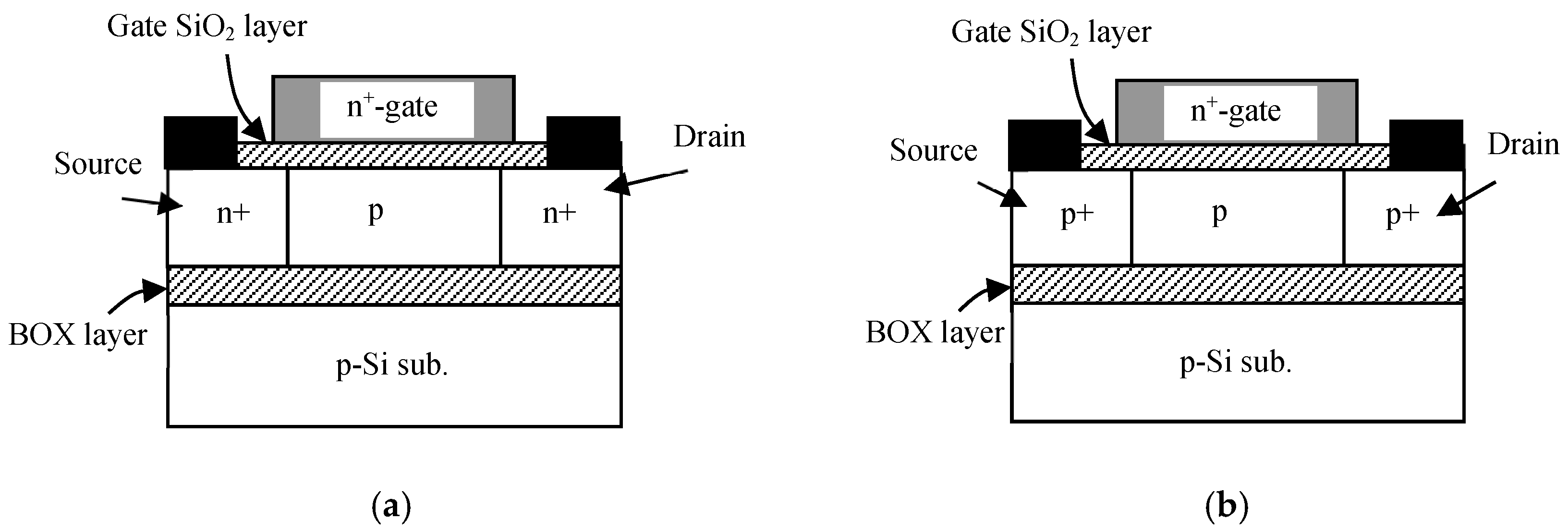
A schematic view of the SOI MOS device structures used in the experiments is shown in Figure 1 [41]; the SOI layer (tS) is 30 nm thick, the gate oxide layer (tOX) is 7 nm thick, the buried-oxide (BOX) layer (tBOX) is 80 nm thick, the body-doping concentration (NA) is 5 × 1017 cm−3 (n-ch MOSFET) or 4 × 1017 cm−3 (p-ch MOSFET) of acceptor Boron atoms, and the gate length (LG) is 0.1 m or 1.0 m. The n-ch MOSFET and p-ch MOSFET have different doping levels (NA) such that the absolute values of their threshold voltages are nominally the same. The channel length (Leff) of the 0.1-μm-long gate device is 40 nm, while that of the 1.0-μm-long gate device is 0.95 m. Primary device parameters are summarized in Table 1. The SOI substrates used here were fabricated in the 1990s. Therefore, not only the SOI layer/buried oxide layer interface quality, but also the gate oxide/SOI layer interface quality is only mediocre. As a result, the trap density is larger than expected as is mentioned later.
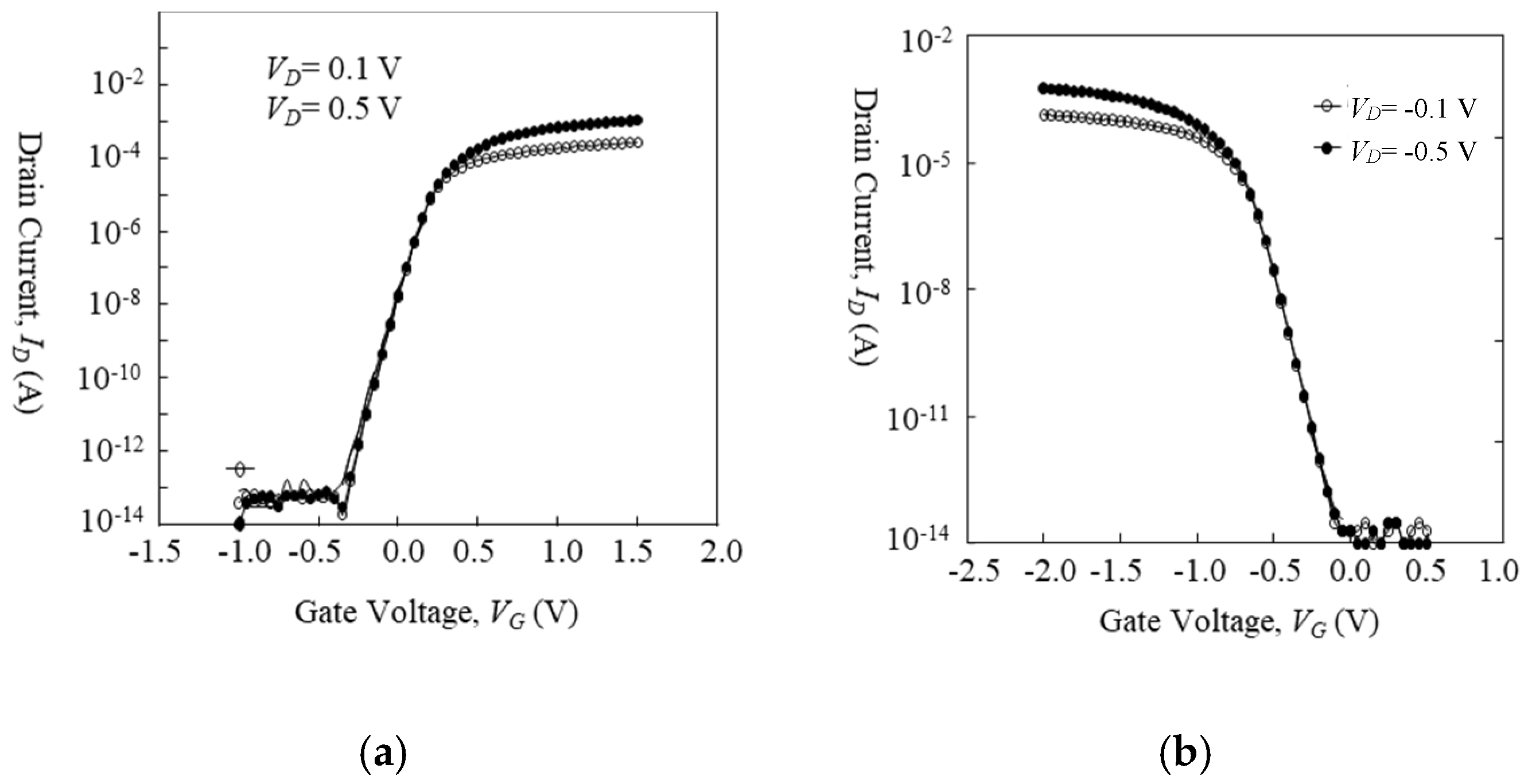
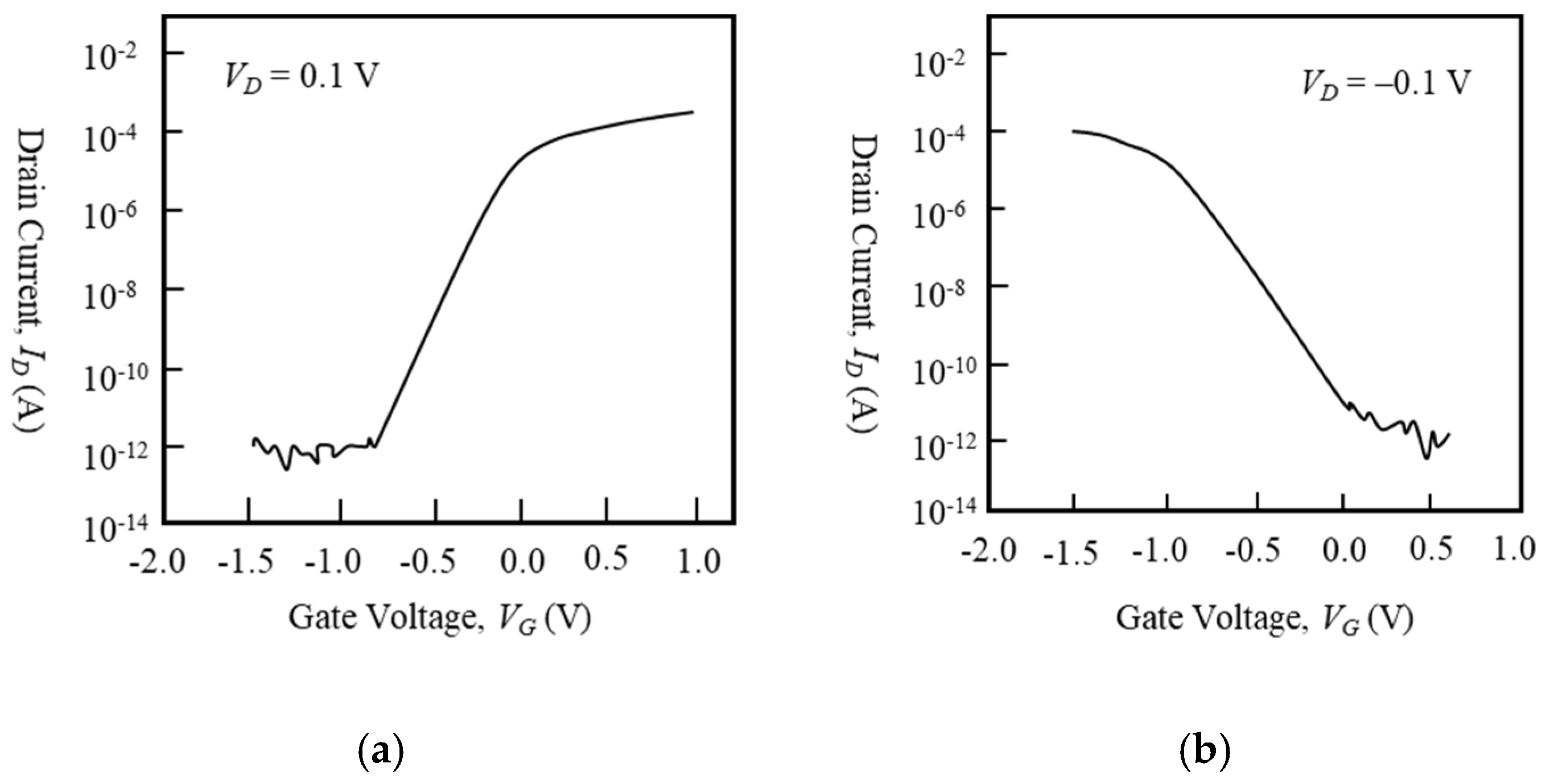
Before discussing LFN behaviors, ID vs. VG characteristics of devices at the bias condition of LFN measurement are shown in Figure 2 and Figure 3. Figure 2a shows the transfer characteristics of the 1-μm-long gate n-type IC-MOSFET with a 50-μm-long gate width, Figure 2b shows those of the 1-μm-long gate p-type BC-MOSFET with a 50-μm-long gate width, Figure 3a shows that of the 100-nm-long gate n-type IC-MOSFET with a 20-μm-long gate width [41], and Figure 3b shows that of the 100-nm-long gate p-type BC-MOSFET with a 20-μm-long gate width [41]. Although the 100-nm-long gate devices exhibit some slight short-channel effect [41], it does not influence the measurement.
To measure LFN characteristics, the wafer on which the semiconductor devices were fabricated was set on the vacuum chuck. The vacuum chuck was entirely covered with a metal frame to provide electromagnetic shielding; the power supply and current sensing were performed by an Agilent 4156C semiconductor parameter analyzer (Agilent Technologies, Santa Clara, CA, USA) without any preamplifier.
When measuring the drain-current fluctuation of n-channel MOSFETs, +100 mV was applied to the drain terminal. A negative bias was applied to that of the p-channel MOSFETs. The drain current fluctuation was measured from the subthreshold current range to ON-current range. A 900-second measurement of current fluctuation was carried out for every device in order to capture comprehensive sets. Although some people divide the raw data into several parts in order to average them, this paper does not apply the method because it violates the mathematical logic of Fourier transformation. The current level of each device under test was chosen to be higher than 10−12 A because the noise current level of the measurement system was ~10−13 A in the subthreshold current range.
The following discussions assume that:
where C(VG, VD, Vsub) is a function that depends on the geometrical parameters of devices, gate voltage (VG), drain voltage (VD), and substrate voltage (Vsub). Parameter γ denotes the exponent of the frequency. In the following section, the measured drain current fluctuations is demonstrated and then theoretical models for the function C(VG, VD, Vsub) are proposed in the subthreshold current range of SOI MOSFETs.
3. Results and Discussion
3.1. Aspects of the Low-Frequency Noise in Long-Channel Silicon-on-Insulator Metal-Oxide-Semiconductor Field-Effect Transistor (SOI MOSFETs)
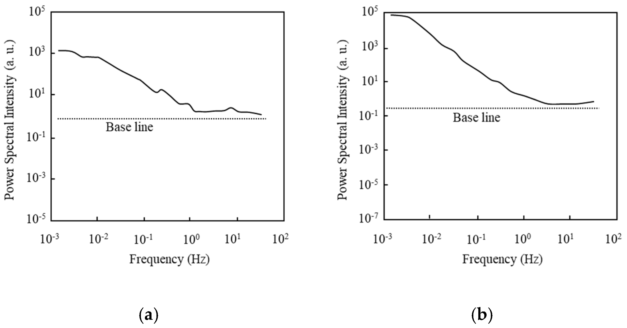
First of all, the basic aspects of the drain current fluctuation of the 1-μm-gate SOI MOSFET are investigated. Before characterizing the normalized current fluctuation power spectral intensity () of the drain current, the frequency spectra of obtained in a subthreshold current range are shown in Figure 4; Figure 4a shows data for the n MOSFET and Figure 4b for the pMOSFET. The baseline is shown to reveal that the value of at 0.1 Hz is higher than the background noise level. Each value is different because the measurement condition of the drain current is different. Figure 4 reveals that the value in Equation (1) is larger than unity.
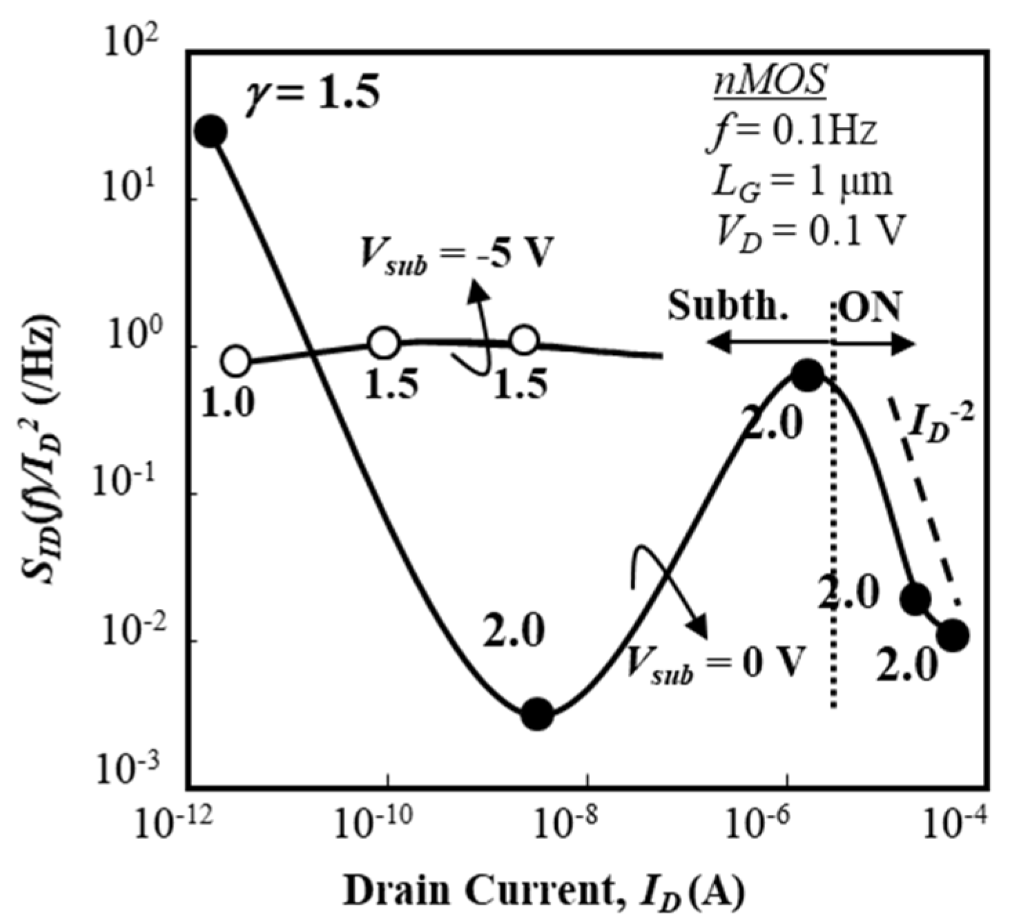
Normalized current fluctuation power spectral intensity () of the drain current of an n-channel IC-MOSFET as a function of drain current (ID) is shown in Figure 5 for two substrate bias conditions (Vsub = 0 V, –5 V). In Figure 5, values of are extracted from the raw data by the parameter fitting technique and their average values are shown. Since the electric field of SOI/buried-oxide layer interface influences the drain current, numerical simulations were carried out in order to estimate the electric field of the buried-oxide layer. This electric field is estimated, at Vsub = 0 V, to be 2.3 × 10⁵ V/cm at ID of 10−12 A and 2.7 × 10⁵ V/cm at ID of 10−6 A. At Vsub = –5 V, its value is 8.0 × 10⁵ V/cm at ID of 10−12 A and 8.3 × 10⁵ V/cm at ID of 10−6 A. Since these electric field conditions suggest that the SOI/buried-oxide interface does not deplete holes even when Vsub = 0 V due to a small work-function difference between the SOI layer and the substrate, it is expected that electron-related traps around the SOI/buried-oxide interface don’t contribute to the low-frequency noise of the front channel (electron current).
It is seen that reveals a deep depression around ID ~10−8 A for Vsub = 0 V. This aspect also appears in sub-micron gate devices (not shown here [29]). On the “ON” state for the gate voltage (VG) beyond the threshold voltage, is proportional to ID−2 with γ = 2, which strongly suggests that the drain current (electron current) fluctuation is the primary determiner of the carrier density fluctuation due to interface traps [24,25]; it is anticipated that the carrier density fluctuation is due to the interface traps near the top surface of the SOI layer, and that most such traps are effectively shielded by the inversion layer in the “ON” state. On the other hand, is basically insensitive to the drain current level (ID) in the subthreshold bias range for Vsub = –5 V. The behavior of for Vsub = –5 V suggests that the interface traps near the bottom surface of SOI layer are effectively shielded by accumulated holes. In contrast, when Vsub = 0 V, the interface traps near the bottom surface of SOI layer are not sufficiently shielded, and some of the electrons contributing to the subthreshold conduction are trapped near the bottom surface. Since the SOI layer thickness is less than the Debye length in this situation, it is expected according to the theoretical model proposed by V. A. Kochelap et al. [42,43] that Coulomb interactions between surface electrons and charged interface traps at the bottom surface may suppress the subthreshold current fluctuation because the surface-noise-suppression factor defined by them increases.
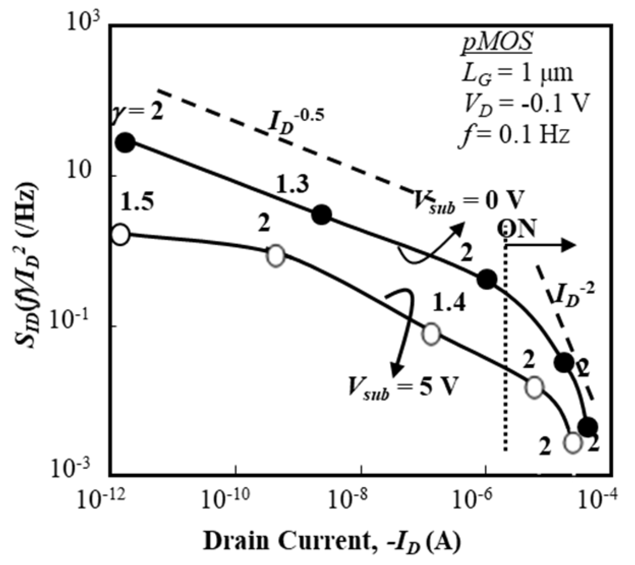
Normalized fluctuation power spectral intensity () of the drain current of a p-channel BC-MOSFET as a function of drain current (ID) is shown in Figure 6 for two substrate bias conditions (Vsub = 0 V, 5 V). In Figure 6, values of () are extracted from the raw data by the parameter fitting technique and their average values are shown. Since the electric field of the SOI/buried-oxide layer interface influences the drain current, numerical simulations were carried out for the p-channel BC-MOSFET in order to estimate the electric field of the buried oxide layer. This electric field is estimated, at Vsub = 0 V, to be 1.7 × 10⁵ V/cm at ID of 10−12 A and 3.9 × 10⁵ V/cm at ID of 10−6 A. At Vsub = 5 V, it is 4.0 × 10⁵ V/cm at ID of 10−12 A and 4.4 × 10⁵ V/cm at ID of 10−6 A. When Vsub = 0 V, the effective buried-oxide electric field slightly lowers the threshold voltage of the p-channel BC-MOSFET. When Vsub = 5 V, the electric field of the buried-oxide layer depletes holes from the SOI/buried-oxide interface, which raises the threshold voltage of the p-channel BC-MOSFET; in other words, it is expected that a hole channel will be generated near the top surface of the SOI layer. As a result, it is anticipated that hole-related traps around the SOI/buried-oxide layer do not contribute to the low-frequency noise of the p-channel BC-MOSFET for Vsub = 5 V. Therefore, Vsub dependence of () is reasonable.
It is seen that () exhibits the drain current dependence of ID−0.5 regardless of substrate bias in the subthreshold bias range, although the magnitude of () is reduced if the substrate bias is positive. This suggests that some interface traps of the buried oxide layer do not contribute to the noise because the SOI/buried-oxide layer interface is depleted for Vsub = 5 V. The conventional idea suggests that bulk traps of the SOI layer contribute to the current fluctuation because the buried channel width expands as the gate voltage rises, and/or that interface traps near the top surface of the SOI layer and/or near the bottom surface of the SOI layer contribute to the current fluctuation; however, this is not the case. This behavior, seen in Figure 6, is also observed in sub-micron gate devices (not shown here [29]). In the “ON” state with gate voltages (VG) beyond the threshold voltage, is proportional to ID−2 with γ = 2, which strongly suggests that the drain current (hole current) fluctuation is primarily responsible for the carrier density fluctuation due to the interface traps near the top surface of the SOI layer [26,27] because the major part of the hole current consists of the hole accumulation layer near the front gate oxide layer for VG > VTH, where VTH is the threshold voltage. It is considered that the impact of interface traps on the drain current fluctuation is almost the same as that on the inversion channel, although it is anticipated that some traps near the top surface of the SOI layer are shielded by the hole accumulation layer. This consideration is utilized in deriving the theoretical model detailed later.
Past work focused on developing theoretical models for the “ON” state [3,4,5,6,11,12,13,15,16,17,18,19,20,26]. A recent model [27] has been written as:
where αc denotes the scattering factor [11], λ denotes the effective tunneling distance, and Nt denotes the effective trap density (cm−2∙eV−1). Parameter αc is an empirical parameter, not a physics-based parameter. For the “ON” state shown in Figure 5 and Figure 6, Equations (2) and (3) suggest that trap density Nt is roughly constant in this gate-voltage range for both the IC-MOSFET and BC-MOSFET. This speculation is acceptable because the local Fermi level at the top surface of the SOI layer is still slightly above midgap for the n-ch IC-MOSFET and the local Fermi level at the top surface of the SOI layer is slightly below the Fermi level in the flat-band condition for the p-ch BC-MOSFET. In other words, this suggests that the distribution of Nt over the energy gap of Si definitely controls the behavior of Equation (2).
Although the noise behavior in the subthreshold bias range must be considered, no corresponding physics-based theoretical models have been proposed. This paper corrects this deficiency in a later section.
3.2. Aspects of Low-Frequency Noise in 100-nm-long Gate SOI MOSFETs
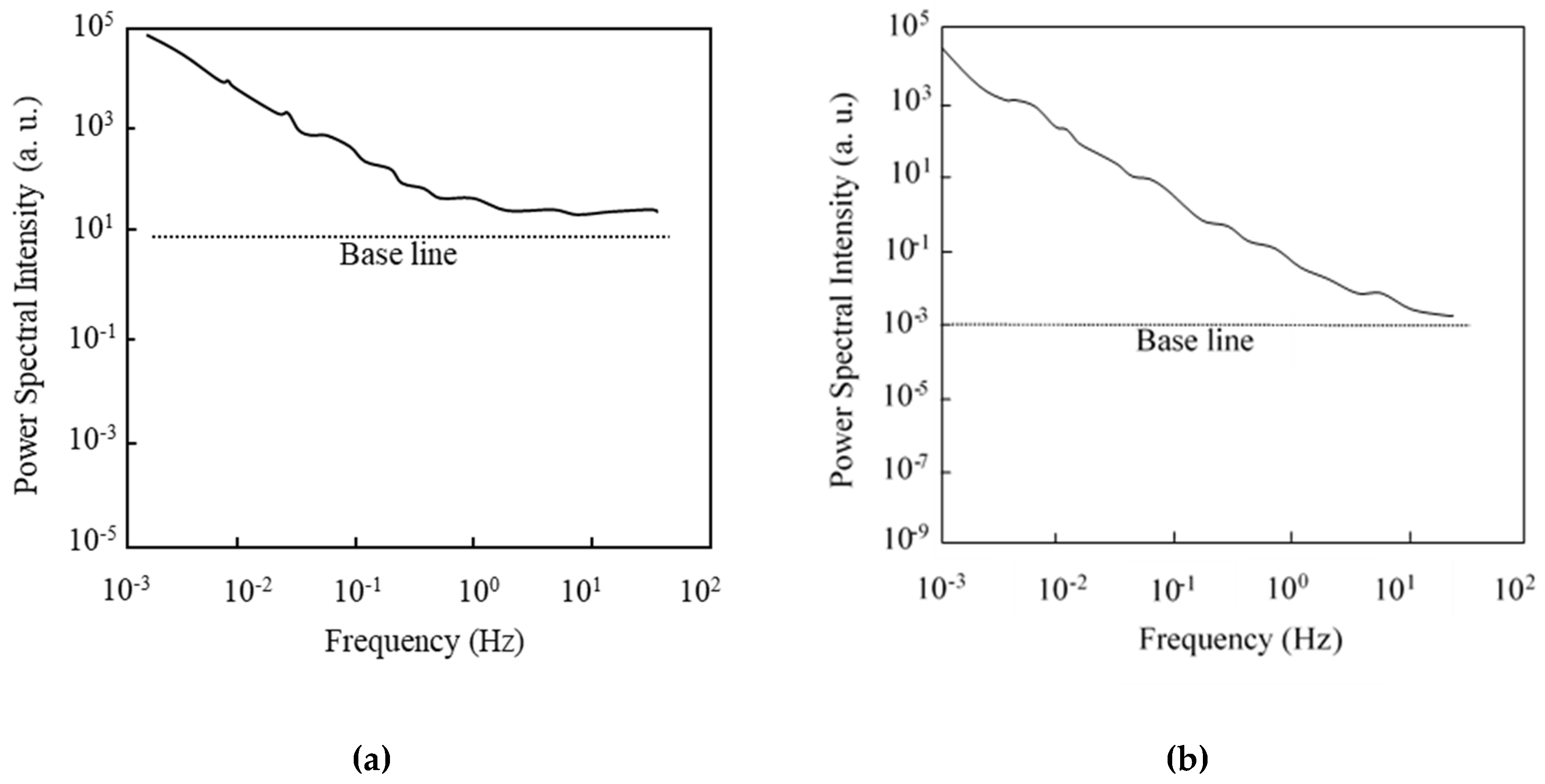
Before characterizing the normalized current fluctuation power spectral intensity () of drain current, the frequency spectra of obtained in a subthreshold current range are shown in Figure 7; Figure 7a shows the nMOSFET data and Figure 7b shows MOSFET data. Figure 7 reveals that the γ value in Equation (1) is larger than unity. Normalized fluctuation power spectral intensity () of the drain current of an n-channel IC-MOSFET with 100-nm-long gate (40-nm-long channel) [44] is shown in Figure 8 as a function of drain current (ID) for two substrate bias conditions (Vsub = 0 V, –5 V). In Figure 8, values of are extracted from the raw data by the parameter fitting technique and their average values are shown. is insensitive to the drain current in the subthreshold bias range regardless of the substrate bias. The behavior of for Vsub = 0 V is very different from that shown in Figure 5; no depression in is observed. These behaviors of the 100-nm gate device suggest the following points.
(1) In the subthreshold bias range, the contribution of traps far from the top surface of the SOI layer to the current fluctuation is quite limited, which is anticipated from the insensitivity of to the substrate bias. This behavior is different from that of long-channel devices, see Figure 5.
(2) Above the threshold voltage, is proportional to ID−2. Equation (2), for example, suggests that the SVFB factor is roughly constant above the threshold voltage, see Figure 8, when ID is increased with a constant VD value because the ID value is increased when VG is increased. This suggests that the trap density profile near the midgap is almost flat because the local Fermi level at the top surface of the SOI layer is located around the midgap.
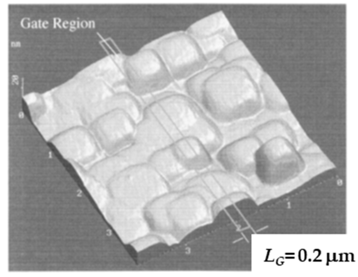
The surface morphology of the buried oxide layer of the MOSFETs used in this experiment has a specific mesa shape aligned to the [100] direction [45,46]; the mesa scale is about 500 nm × 500 nm (in plane) as shown in Figure 9. It is considered that the local fluctuation of the surface potential rules the carrier conduction path in the subthreshold current range [47]. Therefore, it is easily anticipated that the local surface potential of the SOI layer of the MOSFET used here is modified by SOI layer thickness fluctuation [48]. In the present case, it is expected that the spatial uniformity of SOI layer thickness is limited to an area of at most 300 nm × 300 nm, which suggests that the local uniformity of interface trap density is also limited to an area of at most 300 nm × 300 nm. Therefore, the behavior of the 100-nm-gate MOSFET is more insensitive to the substrate bias than that of the long-channel MOSFET.
Next, normalized fluctuation power spectral intensity () of the drain current of a p-channel BC-MOSFET as a function of drain current (ID) is shown in Figure 10 for two substrate bias conditions (Vsub = 0 V, 5 V) [49]. The magnitude of shows a weak dependence on ID (~ID−1/2) in the subthreshold current range regardless of the substrate bias. The behavior of is roughly the same as those shown in Figure 6, but it does show a strong dependence on ID (~ID−5) in the “ON” state. These behaviors of the 100-nm-long gate BC-MOS device suggest the following points.
(1) It is anticipated that the current fluctuation in the subthreshold bias range originates from interface traps near the top surface of the SOI layer, not primarily from interface traps near the bottom interface of the SOI layer.
(2) Following Equation (2), it seems that the trap density energy profile near the top surface of the SOI layer is almost flat, but its value slightly decreases when the local Fermi level of the top surface of the SOI layer approaches the midgap from the level above the midgap because decreases (~ID−1/2) as ID increases.
(3) The contribution of interface traps existing near the bottom surface of the SOI layer to the current fluctuation is not so significant, which is supported by the fact that the magnitude of is insensitive to positive substrate bias values. On the other hand, the behavior of in the “ON” state reveals that the impact of interface traps near the top surface of the SOI layer on the channel current is greatly suppressed, which is suggested by the very steep decrease in in the “ON” state. The channel current formed in the surface hole accumulation layer is basically not influenced by the interface traps near the top surface of the SOI layer because the hole density is very high. This suggests that the surface accumulation layer effectively shields hole traps near the valence band edge.
4. Theoretical Modeling for Subthreshold Current Fluctuations
4.1. Inversion-Channel MOSFET
Subthreshold current of the n-channel IC-MOSFET at the top surface is given by [50]:
where ϕss denotes the top surface potential, ES denotes the surface electric field, and we assume VD <kBT/q. Other notations follow the conventional terminology. Here, the theoretical formulation follows Langevin’s method [51]. When we assume that the noise source yields the fluctuation of the front surface potential (ϕss), whereas the drain current fluctuation δID originates from δφss. Starting with Equation (4), δID is given as:
Then we have,
where <X> means the time averaging of the parameter X. The spectral density of drain current fluctuation is calculated as:
Sϕss(f) corresponds to the surface potential fluctuation power spectral intensity. It is frequently thought that Sϕss(f) stems from the carrier density fluctuation [2,11]. One possible source of Sϕss(f) is the trapping-detrapping process of carriers near the top surface of the silicon layer. This expression is valid for ϕss > 0; that is ID >ISth.
4.2. Buried-Channel MOSFET
On the other hand, the subthreshold current of the p-channel BC-MOSFET near the bottom surface or the top surface is given by [52]
where ϕSS denotes the top surface potential, ϕBS denotes the bottom surface potential, and we assume VD < kBT/q. Equation (10) can be approximated as:
F(ϕSS) is given as [41],
and we have,
Parameter fC partially represents the capacitance coupling effect. Here CS denotes the SOI layer capacitance, CBOX denotes the buried oxide layer capacitance, and V*SUB denotes the effective substrate bias.
Assuming that the current fluctuation originates from the traps near the top surface of the silicon, we can say that the surface potential fluctuation directly influences the bottom surface potential fluctuation electrostatically. The theoretical calculation is based on the same approach mentioned in Section 4.1. This argument yields the following expression for the power spectral intensity of the fluctuation of the buried-channel current.
corresponds to the fluctuation power spectral intensity of the top surface potential.
Taking account of the fact that IBS >> ISS, Equation (16) can be rewritten as:
On the other hand, when it is assumed that the current fluctuation originates from the traps near not only the top surface, but also the bottom surface, of the SOI layer, we have the following expression for the power spectral intensity of the fluctuation of the buried-channel current [51].
where corresponds to the fluctuation power spectral density of bottom surface potential. It is assumed that because IBS >> ISS. Thus we have:
4.3. Theoretical Modeling of Fluctuation Sources and Brief Examination of the Model
Following the conventional idea, it can be assumed that the fluctuation source for the current fluctuation originates from the trapping–detrapping process of Si/SiO2 interface states [1,2,27]. The top surface potential fluctuation <ϕSS2> can be written as [2,44]:
where Nt(EF) denotes the trap density at the local Fermi level, COX is the gate oxide capacitance per unit area, and η is the parameter (units of frequency) that is used in order to adjust the physical dimension of Sϕss(f). The local Fermi level at the top surface of the SOI layer is a function of the surface potential, ϕSS. Other than parameter λ, Equation (20) is basically the same as Equation (3).
In Figure 8, normalized fluctuation power spectral intensity () of the drain current of n-channel IC-MOSFETs is almost constant and insensitive to ID when Vsub = –5 V. Since the bottom surface of the SOI layer is electrostatically shielded by holes when Vsub = –5 V, the electron current near the top surface of the SOI layer is influenced primarily by the interface traps near the top surface of the SOI layer. As Equation (8) is not sensitive to ϕSS, Figure 8 suggests that Nt(EF) is almost flat around the midgap. This speculation is reasonable because EF approaches the conduction band bottom via the midgap when the gate voltage approaches the threshold voltage.
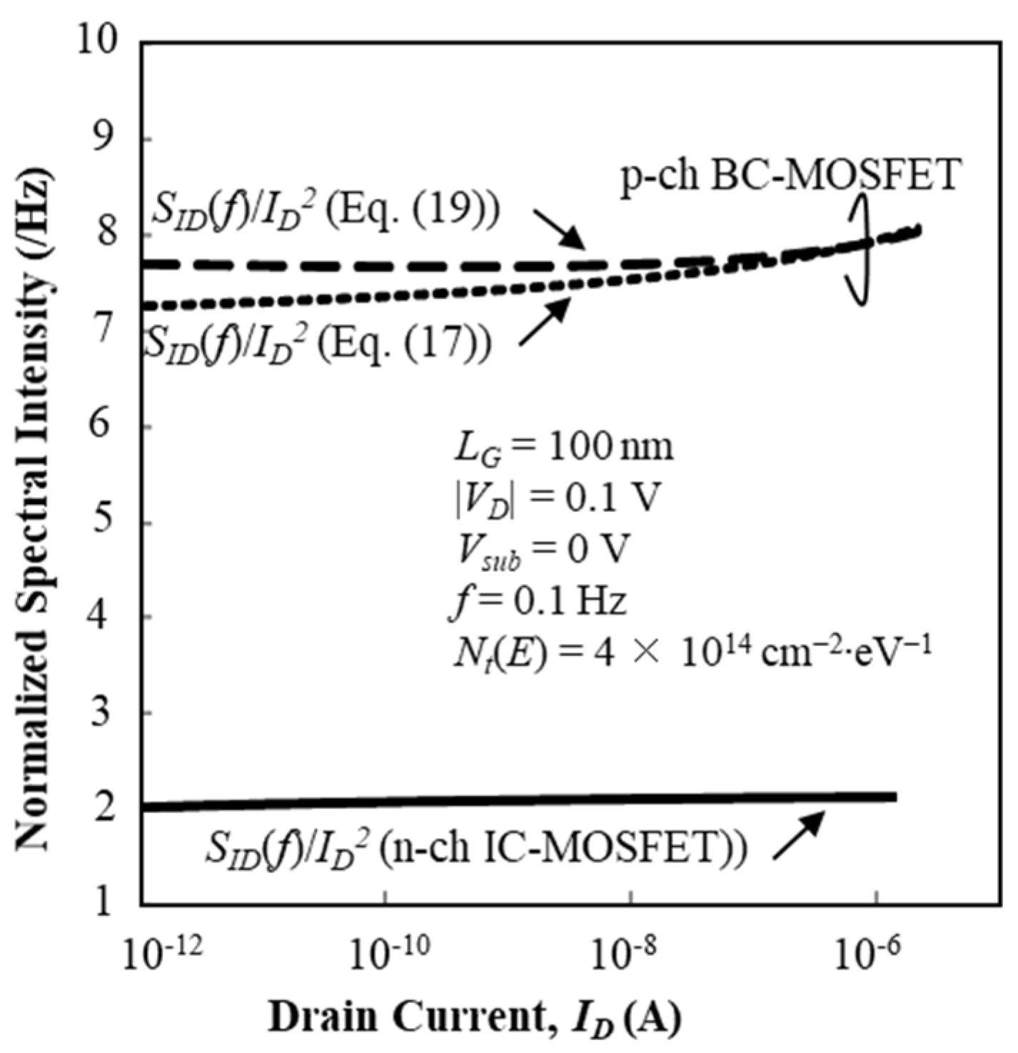
Calculation results of normalized fluctuation power spectral intensity () of the drain current of the n-channel IC-MOSFET are plotted as a function of ID by solid lines in Figure 11 for Vsub = 0 V and Figure 12 for Vsub = –5 V, where it is assumed that Nt(E) is constant with the value of 4 × 1014 cm−2∙eV−1. The effective trap density is about 1 × 1013 cm−2 at room temperature. Calculation results of for the n-channel IC-MOSFET are insensitive to Vsub, and the values and behavior insensitivity to ID well match the experimental results. Therefore, Equation (8) successfully predicts the characteristics in the subthreshold bias range.
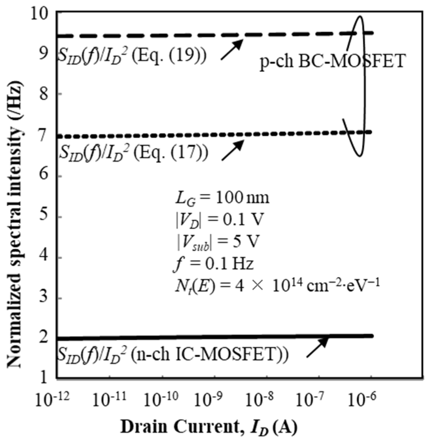
On the other hand, we show two calculation results of the normalized fluctuation power spectral intensity () of the drain current of the p-channel BC-MOSFET as a function of ID in Figure 11 for Vsub = 0 V and Figure 12 for Vsub = 5 V, where it is assumed that Nt(E) is constant with value of 4 × 1014 cm−2∙eV−1. The effective trap density is about 1 × 1013 cm−2 at room temperature. In Figure 11 and Figure 12, results of Equation (17) are shown by dotted lines and those of Equation (19) are shown by broken lines. calculated by Equation (17) decreases with positive substrate bias as seen in Figure 12. However, calculated by Equation (19) increases with positive substrate bias, see Figure 12. This assessment reveals that model Equation (17) is acceptable, which means that the current fluctuation of BC-MOSFETs is primarily ruled by the interface traps near the top surface of the SOI layer. This new finding is given by the theoretical analysis proposed in this paper. Equation (17) successfully predicts the characteristics in the subthreshold bias range. Finally, we examined whether the value of Nt(E) alters the substrate bias dependence of assuming the adoption of Equations (17) and (19). When Nt(E) = 4 × 1013 cm−2∙eV−1, values are reduced to one tenth that for Nt(E) = 4 × 1014 cm−2∙eV−1 because the surface potential fluctuation is proportional to Nt(E) (see Equation (20)). However, the substrate bias dependence of does not change.
5. Conclusions
This paper elucidated the normalized drain current fluctuation spectral intensity of various long-channel and short-channel SOI MOSFETs (inversion-channel SOI MOSFETs and buried-channel SOI MOSFETs) from the viewpoint of scaling. This paper reconsidered low-frequency noise behavior in the inversion-channel SOI MOSFET and the buried-channel SOI MOSFET because it is anticipated that the quality of both Si/SiO2 interfaces should modulate the low-frequency noise characteristics of both devices. Our assessments also addressed the low-frequency noise behavior of sub-100-nm-long channel SOI MOSFETs. The low-frequency noise behavior in the subthreshold bias range was discussed in some detail in order to consider device suitability for future low-voltage and low-power applications.
This paper also proposed theoretical models to explain and predict the drain current fluctuations of SOI MOSFETs. For the buried-channel device, two models were proposed; one assumes that the drain current fluctuation originates from the traps near the top surface of the SOI layer, and the other assumed that the drain current fluctuation originates from the traps near the bottom surface of the SOI layer. As expected, the analyses showed that the current fluctuation of the inversion channel SOI MOSFET is strongly influenced by interface traps near the top surface of the SOI layer because those traps are not well shielded by surface weak inversion carriers in the subthreshold bias range. However, unexpectedly, the buried channel is primarily influenced by interface traps near the top surface of the SOI layer, not by traps near the bottom surface of the SOI layer. This interesting characteristic of current fluctuation spectral intensity was well explained by the theoretical models proposed here. One theoretical expression reveals that the impact of substrate bias is not due to just the capacitance coupling effect, which contradicts the conventional model. As a result, the interface trap density of the top surface of the SOI layer should be reduced in order to improve the analog performance of SOI MOSFETs.
Funding
A part of this study is financially supported by Kansai University Grants, 2015.
Acknowledgments
The author wishes to express his thanks to Shingo Sato and the undergraduate students in the laboratory for their technical support and discussion.
Conflicts of Interest
The author declares no conflict of interest. The funders had no role in the design of the study; in the collection, analyses, or interpretation of data; in the writing of the manuscript; or in the decision to publish the results.
References
- McWhorter, A.L. Semiconductor Surface Physics; Kingston, R.H., Ed.; University of Pennsylvania Press: Philadelphia, PA, USA, 1957; p. 207. [Google Scholar]
- Sah, C.T.; Hielsher, F.H. Evidence of the Surface Origin of the 1/f Noise. Phys. Rev. Lett. 1966, 17, 956–958. [Google Scholar] [CrossRef]
- Klaassen, F.M. Characterization of low 1/f noise in MOS transistors. IEEE Trans. Electron. Devices 1971, 18, 887–891. [Google Scholar] [CrossRef]
- Hooge, F.N. 1/f Noise. Physica 1976, 83, 14–23. [Google Scholar] [CrossRef]
- Kleinpenning, K.G.M.; Vandamme, L.K.J. Model for 1/f Noise in Metal-Oxide-Semiconductor Transistors. J. Appl. Phys. 1981, 52, 1594–1596. [Google Scholar] [CrossRef]
- Jindal, R.P.; Van der Ziel, A. Phonon fluctuation model for flicker noise in elemental semiconductors. J. Appl. Phys. 1978, 52, 2884–2888. [Google Scholar] [CrossRef]
- Handel, P.H. 1/f Noise—An “Infrared” Phenomenon. Phys. Rev. Lett. 1975, 34, 1492–1495. [Google Scholar] [CrossRef]
- Handel, P.H. Quantum Approach to 1/f Noise. Phys. Rev. A 1980, 22, 745–757. [Google Scholar] [CrossRef]
- Van der Ziel, A.; Handel, P.H.; Zhu, X.; Duh, K.H. A Theory of the Hooge Parameters of Solid-State Devices. IEEE Trans. Electron Devices 1985, 32, 667–671. [Google Scholar] [CrossRef]
- Handel, P.H. Fundamental quantum 1/f noise in semiconductor devices. IEEE Trans. Electron Devices 1994, 41, 2023–2033. [Google Scholar] [CrossRef]
- Hung, K.K.; Ko, P.K.; Hu, C.; Cheng, Y.C. A unified model for the flicker noise in metal-oxide-semiconductor field-effect transistors. IEEE Trans. Electron Devices 1990, 37, 654–665. [Google Scholar] [CrossRef]
- Stephany, J.F. A Theory of 1/f Noise. J. Appl. Phys. 1998, 83, 3139–3143. [Google Scholar] [CrossRef]
- Kiss, L.B.; Heszler, P. An Exact Proof of the Invalidity of ‘Handel’s Quantum 1/f Noise Model’, based on Quantum Electrodynamics. J. Phys. C Solid State Phys. 1986, 19, 631–633. [Google Scholar] [CrossRef]
- Nieuwenhuizen, T.M.; Frenkel, D.; van Kampen, N.G. Objection to Handel’s Quantum Theory of 1/f Noise. Phys. Rev. A 1987, 35, 2750–2753. [Google Scholar] [CrossRef]
- Van Vliet, C.M. A survey of results and future prospects on quantum 1/ƒ noise and 1/ƒ noise in general. Solid State Electron. 1991, 34, 1–21. [Google Scholar] [CrossRef]
- Vandamme, E.P.; Vandamme, L.K.J. Critical Discussion on Unified 1/f Noise Models for MOSFETs. IEEE Trans. Electron Devices 2000, 47, 2146–2152. [Google Scholar] [CrossRef]
- Omura, Y. Hooge parameter in buried-channel metal-oxide-semiconductor field-effect transistors. J. Appl. Phys. 2002, 91, 1378–1384. [Google Scholar] [CrossRef]
- Omura, Y. Possible Unified Model for the Hooge Parameter in Inversion-Layer-Channel Metal-Oxide-Semiconductor Field-Effect Transistors. J. Appl. Phys. 2013, 113, 214508–214518. [Google Scholar] [CrossRef]
- Park, H.S.; Van der Ziel, A. Dependence of MOSFET Noise Parameters in n-Channel MOSFETs on Oxide Thickness. Solid State Electron. 1982, 25, 313–315. [Google Scholar] [CrossRef]
- Magnone, P.; Crupi, F.; Giusi, G.; Simoen, E.; Claeys, C.; Pantisano, L.; Maji, D.; Rao, V.R.; Srinivasan, P. 1/f noise in drain and gate current of MOSFETs with high-k gate stacks. IEEE Trans. Device Mater. Reliab. 2009, 9, 180–189. [Google Scholar] [CrossRef]
- Nowak, E.; Kim, J.-H.; Kwon, H.Y.; Kim, Y.-G.; Sim, J.S.; Lim, S.-H.; Kim, D.S.; Lee, K.-H.; Park, Y.K.; Choi, J.-H.; et al. Intrinsic Fluctuations in Vertical NAND Flash Memories. In Proceedings of the 2012 Symposium on VLSI Technology (VLSIT), Honolulu, HI, USA, 12–14 June 2012; pp. 21–22. [Google Scholar]
- Miki, H.; Yamaoka, M.; Frank, D.J.; Cheng, K.; Park, D.-G.; Leobandung, E.; Torii, K. Voltage and Temperature Dependence of Random Telegraph Noise in Highly Scaled HKMG ETSOI nFETs and its Impact on Logic Delay Uncertainty. In Proceedings of the 2012 Symposium on VLSI Technology (VLSIT), Honolulu, HI, USA, 12–14 June 2012; pp. 137–138. [Google Scholar]
- Chen, J.; Hirano, I.; Tatsumura, K.; Mitani, Y. Comprehensive Investigations on Neutral and Attractive Traps in Random Telegraph Signal Noise Phenomena using (100)- and (110)-Orientated CMOSFETs. In Proceedings of the 2012 Symposium on VLSI Technology (VLSIT), Honolulu, HI, USA, 12–14 June 2012; pp. 141–142. [Google Scholar]
- Wei, C.; Jiang, Y.; Xiong, Y.-Z.; Zhou, X.; Singh, N.; Rustagi, S.C.; Lo, G.Q.; Kwong, D.-L. Impact of Gate Electrodes on 1/f Noise of Gate-All-Around Silicon Nanowire Transistors. IEEE Electron Devices Lett. 2009, 30, 1081–1083. [Google Scholar]
- Ioannidis, E.G.; Theodorou, C.G.; Karatsori, T.A.; Haendler, S.; Dimitriadis, C.A.; Ghibaudo, G. Drain-Current Flicker Noise Modeling in nMOSFETs From a 14-nm FDSOI Technology. IEEE Trans. Electron Devices 2015, 62, 1574–1579. [Google Scholar] [CrossRef]
- Ghibaudo, G.; Roux, O.; Nguyen-Duc, C.; Balestra, F.; Brini, J. Improved Analysis of Low Frequency Noise in Field-Effect MOS Transistors. Phys. Stat. Sol. 1991, 124, 571–581. [Google Scholar] [CrossRef]
- Ghibaudo, G. Impact of Device Scaling on LF Noise in CMOS Technologies. In Proceedings of the 17th International Conference Mixed Design of Integrated Circuits and Systems, Prague, Czech Republic, 1–4 June 2003; pp. 301–308. [Google Scholar]
- Rhayem, J.; Rigaud, D.; Eya’a, A.; Valenza, M. 1/f Noise in Metal-Oxide-Semiconductor Transistors Biased in Weak Inversion. J. Appl. Phys. 2001, 89, 4192–4194. [Google Scholar] [CrossRef]
- Ito, T.; Sato, S.; Omura, Y. Characterization of Noise Behavior of Ultrathin Inversion-Channel and Buried-Channel SOI MOSFETs in the Subthreshold Bias Range. In Proceedings of the 2014 IEEE International Meeting for Future of Electron Devices, Kansai (IMFEDK), Kyoto, Japan, 19–20 June 2014; pp. 46–47. [Google Scholar]
- Jin, W.; Chan, P.C.H.; Fung, S.K.H.; Ko, P.K. Shot-noise-induced excess low-frequency noise in floating-body partially depleted SOI MOSFET’s. IEEE Trans. Electron Devices 1999, 46, 1180–1185. [Google Scholar] [CrossRef]
- Workman, G.O.; Fossum, J.G. Physical noise modeling of SOI MOSFETs with analysis of the Lorentzian component in the low-frequency noise spectrum. IEEE Trans. Electron Devices 2000, 47, 1192–1201. [Google Scholar] [CrossRef]
- Gross, B.J.; Sodini, C.G. 1/f noise in MOSFETs with ultrathin gate dielectrics. In Proceedings of the 1992 International Technical Digest on Electron Devices Meeting, San Francisco, CA, USA, 13–16 December 1992; pp. 881–884. [Google Scholar]
- Morshed, T.; Devireddy, S.P.; Rahman, M.S.; Celik-Buller, Z.; Tseng, H.-H.; Zlotnicka, A.; Shanware, A.; Green, K.; Chambers, J.J.; Visokay, M.R.; et al. A new model for 1/f noise in high-k MOSFETs. In Proceedings of the 2007 IEEE International Electron Devices Meeting, Washington, DC, USA, 10–12 December 2007; pp. 561–564. [Google Scholar]
- Simoen, E.; Mercha, A.; Claeys, C.; Lukyanchikova, N.; Garbar, N. Critical discussion of the front-back gate coupling effect on the low-frequency noise in fully depleted SOI MOSFETs. IEEE Trans. Electron Devices 2004, 51, 1008–1016. [Google Scholar] [CrossRef]
- Chandrakasan, A.P.; Daly, D.C.; Finchelstein, D.F.; Kwong, J.; Ramadas, Y.K.; Sinangil, M.E.; Sze, V.; Verma, N. Technologies for Ultradynamic Voltage Scaling. Proc. IEEE 2010, 98, 191–214. [Google Scholar] [CrossRef]
- Vitale, S.A.; Wyatt, P.W.; Checka, N.; Kedzierski, J.; Keast, C.L. FESOI Process Technology for Subthreshold-Operation Ultralow-Power Electronics. Proc. IEEE 2010, 98, 333–342. [Google Scholar] [CrossRef]
- Simoen, E.; Andrade, M.G.C.; Almeida, L.M.; Aoulaiche, M.; Caillat, C.; Jurczak, M.; Claeys, C. On the Variability of the Low-Frequency Noise in UTBOX SOI nMOS-FETs. J. Integr. Circ. Syst. 2013, 8, 71–77. [Google Scholar]
- Van Haartman, M.; Oestling, M. Effect of channel positioning on the 1/f noise in silicon-on-insulator metal-oxide semiconductor field-effect transistors. J. Appl. Phys. 2007, 101, 034506–034509. [Google Scholar] [CrossRef]
- Gaubert, P.; Teramoto, A.; Sugawa, S. 1/f Noise Performances and Noise Sources of Accumulation Mode Si(100) n-MOSFETs. In Proceedings of the International Conference on Solid State Devices and Materials, Sapporo, Japan, 27–30 September 2015; pp. 96–97. [Google Scholar]
- Lee, J.-H.; Kim, S.-Y.; Cho, I.; Hwang, S.; Lee, J.-H. 1/f Noise Characteristics of Sub-100 nm MOS Transistors. J. Semicond. Technol. Sci. 2006, 6, 38–42. [Google Scholar]
- Omura, Y.; Nakashima, S.; Izumi, K.; Ishii, T. 0.1-μm-Gate, Ultrathin-Film CMOS Devices Using SIMOX Substrate with 80-nm-Thick Buried Oxide Layer. IEEE Trans. Electron Devices 1991, 40, 675–678. [Google Scholar]
- Kochelap, V.A.; Sokolov, V.N.; Bulashenko, O.M.; Rubi, J.M. Coulomb Suppression of Surface Noise. Appl. Phys. Lett. 2001, 78, 2003–2005. [Google Scholar] [CrossRef]
- Kochelap, V.A.; Sokolov, V.N.; Bulashenko, O.N.; Rubi, J.M. Theory of Surface Noise under Coulomb Correlations between Carriers and Surface States. J. Appl. Phys. 2002, 92, 5347–5358. [Google Scholar] [CrossRef]
- Omura, Y. A simple model for substrate current characteristics in short-channel ultrathin-film metal-oxide-semiconductor field-effect transistors by separation by implanted oxygen. Jpn. J. Appl. Phys. 1995, 34, 4722–4727. [Google Scholar] [CrossRef]
- Omura, Y. Two-Dimensionally Confined Injection Phenomenon at Low Temperatures in Sub-10-nm-Thick SOI Insulated-Gate p-n-Junction Devices. IEEE Trans. Electron Devices 1996, 43, 436–443. [Google Scholar] [CrossRef]
- Ishiyama, T.; Omura, Y. Analysis of Interface Microstructure Evolution in Separation by IMplanted OXygen (SIMOX) Wafers. Jpn. J. Appl. Phys. 2000, 39, 4653–4656. [Google Scholar] [CrossRef]
- Arnold, E. Conduction Mechanisms in Bandtails at the SiO2 Interface. Surf. Sci. 1976, 58, 60–70. [Google Scholar] [CrossRef]
- Omura, Y.; Nagase, M. Low-Temperature Drain Current Characteristics in Sub-10-nm-Thick SOI nMOSFET’s on SIMOX (Separation by IMplanted OXygen) substrates. Jpn. J. Appl. Phys. 1995, 34, 812–816. [Google Scholar] [CrossRef]
- Omura, Y.; Sato, S. Theoretical Models for Low-Frequency Noise Behaviors of Buried-Channel MOSFETs. In Proceedings of the 2017 IEEE SOI-3D-Subthreshold Microelectronics Technology Unified Conference (S3S), Burlingame, CA, USA, 16–19 Octorber 2017. [Google Scholar]
- Sze, S.M.; Ng, K.K. Physics of Semiconductor Devices, 3rd ed.; Wiley: Hoboken, NJ, USA, 2007; p. 314. [Google Scholar]
- Kogan, S. Electronic Noise and Fluctuations in Solids; Cambridge University Press: Cambridge, UK, 1996; Chapter 3. [Google Scholar]
- Omura, Y.; Ohwada, K. Threshold and Subthreshold Characteristics Theory for a Very Small Buried-Channel MOSFET Using a Majority-Carrier Distribution Model. Solid State Electron. 1981, 24, 301–308. [Google Scholar] [CrossRef]
Figure 1.
Schematic silicon-on-insulator (SOI) device structures used in experiments. (a) n-type inversion-channel (IC) metal-oxide-semiconductor field-effect transistors (MOSFET), (b) p-type buried-channel (BC) MOSFET.
Figure 1.
Schematic silicon-on-insulator (SOI) device structures used in experiments. (a) n-type inversion-channel (IC) metal-oxide-semiconductor field-effect transistors (MOSFET), (b) p-type buried-channel (BC) MOSFET.

Figure 2.
ID vs. VG characteristics of 1-μm-long gate MOSFETs. (a) n-type IC-MOSFET, (b) p-type BC-MOSFET. Vsub = 0 V.
Figure 2.
ID vs. VG characteristics of 1-μm-long gate MOSFETs. (a) n-type IC-MOSFET, (b) p-type BC-MOSFET. Vsub = 0 V.

Figure 3.
ID vs. VG characteristics of 100-nm-long gate MOSFETs. (a) n-type IC-MOSFET, (b) p-type BC-MOSFET. Vsub = 0 V.
Figure 3.
ID vs. VG characteristics of 100-nm-long gate MOSFETs. (a) n-type IC-MOSFET, (b) p-type BC-MOSFET. Vsub = 0 V.

Figure 4.
Power spectral intensity of 1.0-μm-long gate SOI MOSFETs at the subthreshold bias. (a) nMOSFET (VD = 0.1 V, VG = –0.4 V, Vsub = 0 V), (b) pMOSFET (VD = –0.1 V, VG = –0.4 V, Vsub = 0 V).
Figure 4.
Power spectral intensity of 1.0-μm-long gate SOI MOSFETs at the subthreshold bias. (a) nMOSFET (VD = 0.1 V, VG = –0.4 V, Vsub = 0 V), (b) pMOSFET (VD = –0.1 V, VG = –0.4 V, Vsub = 0 V).

Figure 5.
Normalized fluctuation power spectral intensity () of drain current as a function of ID in 1-μm gate IC nMOS. LG =1 μm and WG = 50 μm. Substrate voltage (Vsub) is 0 V and –5 V.
Figure 5.
Normalized fluctuation power spectral intensity () of drain current as a function of ID in 1-μm gate IC nMOS. LG =1 μm and WG = 50 μm. Substrate voltage (Vsub) is 0 V and –5 V.

Figure 6.
Normalized fluctuation power spectral intensity () of drain current as a function of ID in 1-μm gate BC pMOS. LG = 1 μm and WG = 50 μm. Substrate voltage (Vsub) is 0 V and +5 V.
Figure 6.
Normalized fluctuation power spectral intensity () of drain current as a function of ID in 1-μm gate BC pMOS. LG = 1 μm and WG = 50 μm. Substrate voltage (Vsub) is 0 V and +5 V.

Figure 7.
Power spectral intensity of 100-nm-long gate SOI MOSFETs at the subthreshold bias. (a) nMOSFET (VD = 0.1 V, VG = –0.6 V, Vsub = 0 V), (b) pMOSFET (VD = –0.1 V, VG = –0.4 V, Vsub = 0 V).
Figure 7.
Power spectral intensity of 100-nm-long gate SOI MOSFETs at the subthreshold bias. (a) nMOSFET (VD = 0.1 V, VG = –0.6 V, Vsub = 0 V), (b) pMOSFET (VD = –0.1 V, VG = –0.4 V, Vsub = 0 V).

Figure 8.
Normalized fluctuation power spectral intensity () of drain current as a function of ID in 100-nm gate IC nMOS. LG = 100 nm and WG = 20 μm. Substrate voltage (Vsub) is 0 V and –5 V.
Figure 8.
Normalized fluctuation power spectral intensity () of drain current as a function of ID in 100-nm gate IC nMOS. LG = 100 nm and WG = 20 μm. Substrate voltage (Vsub) is 0 V and –5 V.
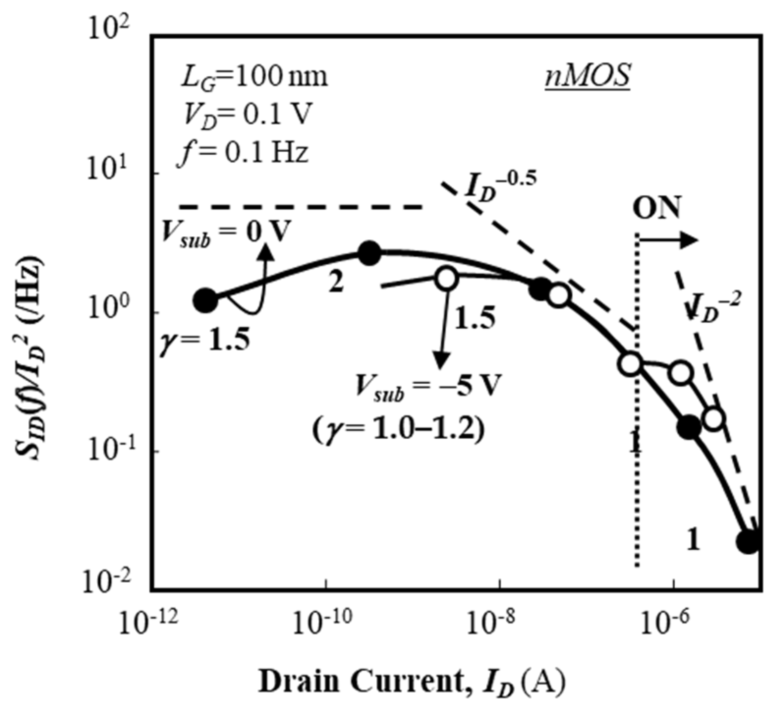
Figure 9.
Atomic force microscopy (AFM) image of surface morphology of the bottom surface of the silicon layer. Reproduced with permission from [45], published by IEEE, 1996.
Figure 9.
Atomic force microscopy (AFM) image of surface morphology of the bottom surface of the silicon layer. Reproduced with permission from [45], published by IEEE, 1996.

Figure 10.
Normalized fluctuation power spectral intensity () of drain current as a function of ID in 100-nm gate BC pMOS. LG = 100 nm and WG = 20 μm. Substrate voltage (Vsub) is 0 V and +5 V. Reproduced with permission from [49], published by IEEE, 2017.
Figure 10.
Normalized fluctuation power spectral intensity () of drain current as a function of ID in 100-nm gate BC pMOS. LG = 100 nm and WG = 20 μm. Substrate voltage (Vsub) is 0 V and +5 V. Reproduced with permission from [49], published by IEEE, 2017.

Figure 11.
Calculation results of as a function of ID for n-channel IC-MOSFET. It is assumed Nt(E) = 4 × 1014 cm−2∙eV−1 and Vsub = 0 V.
Figure 11.
Calculation results of as a function of ID for n-channel IC-MOSFET. It is assumed Nt(E) = 4 × 1014 cm−2∙eV−1 and Vsub = 0 V.

Figure 12.
Calculation results of as a function of ID for p-channel BC-MOSFET. It is assumed Nt(E) = 4 × 1014 cm−2∙eV−1. Vsub = –5 V for nMOSFET and Vsub = +5 V for pMOSFET.
Figure 12.
Calculation results of as a function of ID for p-channel BC-MOSFET. It is assumed Nt(E) = 4 × 1014 cm−2∙eV−1. Vsub = –5 V for nMOSFET and Vsub = +5 V for pMOSFET.


Table 1.
Parameters of fabricated devices.
| Devices | ts | tox | tBOX | NA |
|---|---|---|---|---|
| IC-MOSFET | 30 nm | 7 nm | 80 nm | 5 × 1017 cm−3 |
| BC-MOSFET | 30 nm | 7 nm | 80 nm | 4 × 1017 cm−3 |
© 2018 by the author. Licensee MDPI, Basel, Switzerland. This article is an open access article distributed under the terms and conditions of the Creative Commons Attribution (CC BY) license (http://creativecommons.org/licenses/by/4.0/).
Share and Cite
MDPI and ACS Style
Omura, Y. Empirical and Theoretical Modeling of Low-Frequency Noise Behavior of Ultrathin Silicon-on-Insulator MOSFETs Aiming at Low-Voltage and Low-Energy Regime. Micromachines 2019, 10, 5. https://doi.org/10.3390/mi10010005
AMA Style
Omura Y. Empirical and Theoretical Modeling of Low-Frequency Noise Behavior of Ultrathin Silicon-on-Insulator MOSFETs Aiming at Low-Voltage and Low-Energy Regime. Micromachines. 2019; 10(1):5. https://doi.org/10.3390/mi10010005
Chicago/Turabian StyleOmura, Yasuhisa. 2019. "Empirical and Theoretical Modeling of Low-Frequency Noise Behavior of Ultrathin Silicon-on-Insulator MOSFETs Aiming at Low-Voltage and Low-Energy Regime" Micromachines 10, no. 1: 5. https://doi.org/10.3390/mi10010005
Note that from the first issue of 2016, this journal uses article numbers instead of page numbers. See further details here.