High Performance Drain Engineered InGaN Heterostructure Tunnel Field Effect Transistor

Wide Bandgap Semiconductor Technology Disciplines State Key Laboratory, School of Microelectronics, Xidian University, Xi’an 710071, China
*
Authors to whom correspondence should be addressed.
Micromachines 2019, 10(1), 75; https://doi.org/10.3390/mi10010075
Submission received: 27 December 2018
/
Revised: 18 January 2019
/
Accepted: 18 January 2019
/
Published: 21 January 2019
(This article belongs to the Special Issue Miniaturized Transistors)
Abstract
:A drain engineered InGaN heterostructure tunnel field effect transistor (TFET) is proposed and investigated by Silvaco Atlas simulation. This structure uses an additional metal on the drain region to modulate the energy band near the drain/channel interface in the drain regions, and increase the tunneling barrier for the flow of holes from the conduction band of the drain to the valence band of the channel region under negative gate bias for n-TFET, which induces the ambipolar current being reduced from 1.93 × 10⁻⁸ to 1.46 × 10⁻¹¹ A/μm. In addition, polar InGaN heterostructure TFET having a polarization effect can adjust the energy band structure and achieve steep interband tunneling. The average subthreshold swing of the polar drain engineered heterostructure TFET (DE-HTFET) is reduced by 53.3% compared to that of the nonpolar DE-HTFET. Furthermore, ION increases 100% from 137 mA/mm of nonpolar DE-HTFET to 274 mA/mm of polar DE-HTFET.
1. Introduction
Tunnel field effect transistors (TFETs) have been considered as attractive alternative replacements to metal-oxide-semiconductor field effect transistors (MOSFETs) for low power applications [1,2,3], due to the conductive mechanism of band to band tunneling, realizing a steep subthreshold swing (SS) (less than 60 mV/dec at room temperature), good immunity against Short Channel Effects (SCEs) and high ON-state current (ION) to OFF-state current (IOFF) ratio (ION/IOFF) [1,4,5]. Although TFETs have various benefits, there are still some problems to be solved, such as the ambipolar behavior [6,7], low ON-state current (ION) [8], and less-than-idea SS. To solve these problems, different techniques such as the use of high-k dielectric materials [9], heterojunction engineering [10,11,12,13], source pocket based devices [14,15], junction-less concept based devices [16,17,18], and narrow bandgap materials have been investigated to boost ION. Drain doping profile investigation [7], gate-drain electrode gap control [19], the hetero-dielectric box concept [20], and heterojunction engineering have been developed to restrain ambipolar behavior.
Ш Nitride is the direct bandgap semiconductor, and its bandgap can be modulated from 0.7 eV (InN) to 6.2 eV (AlN), while the natural polarization effect will facilitate the formation of a steep energy band at the tunneling junction of the heterostructure, inducing a steep tunneling junction, small subthreshold swing and large ON-state current [21]. Recently, it has been reported that Ш Nitride TFETs exhibit superior device characteristics, showing the great potential of the application in the low power field [21,22,23,24]. However, the research on Ш Nitride TFET devices is just beginning, and it is worth further study.
In this paper, the drain engineering method uses workfunction engineering on an additional metal to modulate the energy band on the drain/channel interface in the drain regions and increase the tunneling barrier for the flow of holes from the conduction band of the drain to the valence band of the channel region under negative gate bias for n-TFET, which will reduce the ambipolar current of InGaN heterojunction TFETs (HTFETs). In addition, the improvement mechanism of the polarization effect on the subthreshold and ON-state characteristics of polar InGaN HTFETs are investigated at length.
The remaining paper is organized as follows: Section 2 presents the device structure, simulation models and material parameters. Section 3 is dedicated to results and discussions, including the drain engineered TFET used to suppress the ambipolar current of InGaN HTFET, and the performance comparison and analysis of polar and nonpolar HTFETs. Finally, Section 4 concludes the paper with some important findings.
2. Device Structure and Simulation Parameters
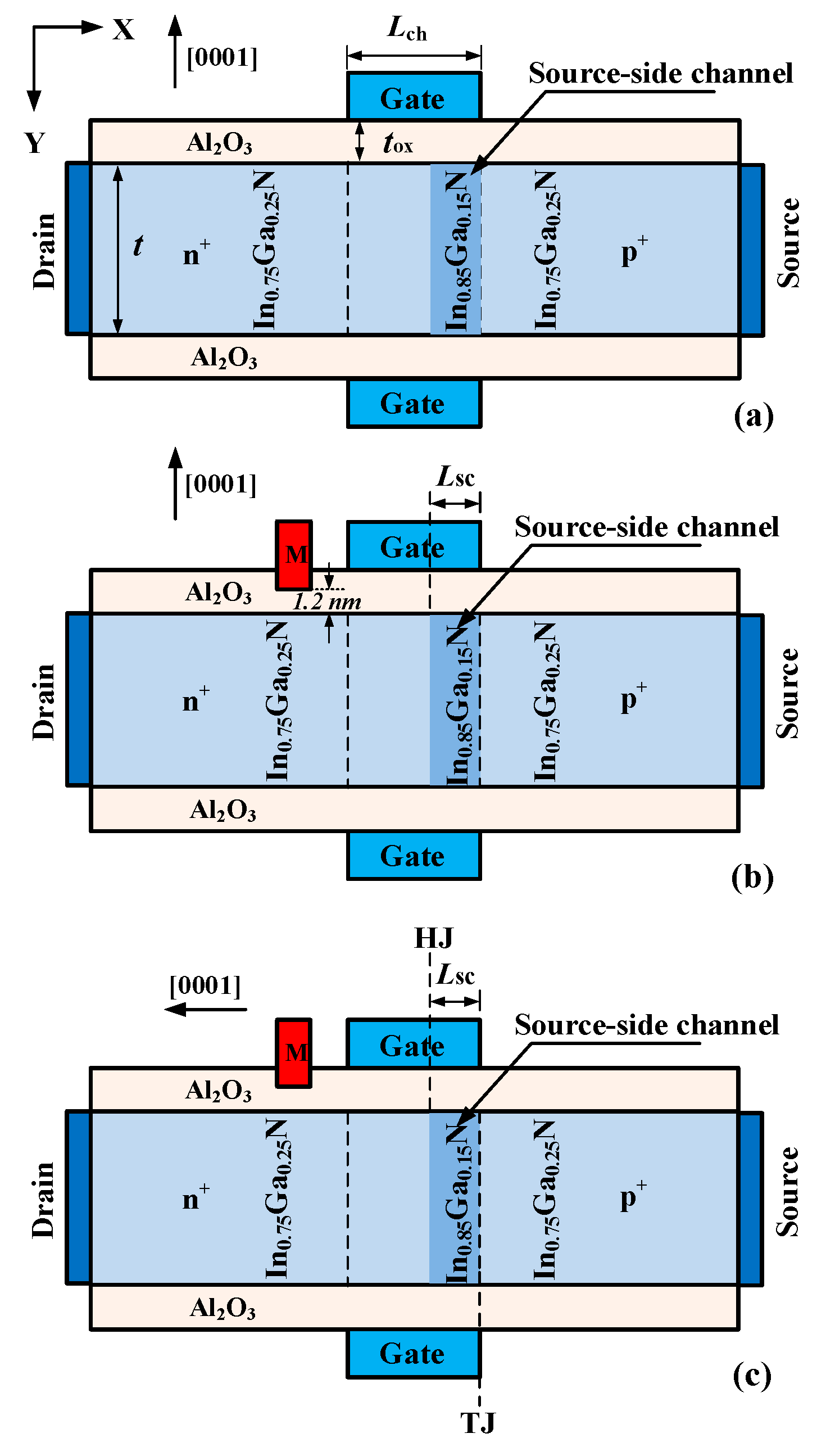
Figure 1 shows the cross-sectional views of InGaN nonpolar heterostructure TFET (HTFET), InGaN nonpolar drain engineered heterostructure TFET (DE-HTFET), and InGaN polar DE-HTFET, respectively. The InGaN HTFET contains a source-side channel to improve the ON-state current and reduce the subthreshold swing. This work has been reported in reference [24]. The channel length (Lch) and the channel thickness (t) are set as 50 nm, and 10 nm, respectively. The drain metal and the gate (LGD) are 100 nm. The gate dielectric material is Al2O3 with a thickness (tox) of 3 nm. The doping concentrations in the source, the channel, and the drain region are p+ 9.9 × 1019 cm−3, n 1 × 1015 cm−3, and n+ 1.2 × 1019 cm−3, respectively. The workfunction of gate metal is 5.1 eV. The proposed nonpolar DE-HTFET contains an additional drain engineering metal with the length of 10 nm and a dielectric thickness of 1.2 nm to modulate the energy band in the drain/channel region and finally reduce the ambipolar current. Along with this, the polar DE-HTFET is proposed to modulate the energy band at the source/channel tunneling junction, and will further improve the device characteristics.
Simulations are carried out using a 2D Silvaco Atlas simulator (5.19.20.R, Silvaco Inc., Santa Clara, CA, USA) [25]. The nonlocal band to-band tunneling (BTBT) is incorporated in the simulation for the calculation of the tunneling rate of charge carriers. The Shockley–Read–Hall (SRH) carrier recombination model, bandgap narrowing (BGN) model, constant low field mobility model, and field-dependent mobility model at high electric fields are activated using the SRH, BGN and FLDMOB parameters, respectively. The polarization effect in the polar TFET is simulated by a fixed polarization charge at the heterojunction interface [26], and the density of polarization surface charge (σpol) will be discussed in Section 3.2. Other material parameters used in the simulations are presented in Table 1.
In the electrical characteristics analysis below, ION is defined to be the drain current ID at VG = VD = 1 V. The average sub-threshold swing (SSavg) is obtained from the ID-VG curve, it is given by
where the threshold voltage VTH is defined to be the gate voltage (VG) at current of 1 × 10⁻⁷ A/mm, and VOFF is the gate voltage at ID of 10−18 A/mm.
3. Results and Discussions
3.1. Drain Engineered HTFET to Suppress Ambipolar Current
3.1.1. Impact of Drain Engineering Metal Position on Electrical Characteristic of DE-HTFET
Drain engineered HTFET using an additional drain engineering metal (M) to modulate the energy band can increase the tunneling barrier for the flow of holes on the drain/channel interface, and reduce the ambipolar current at the negative VG bias. The M position will obviously affect the electrical characteristic of DE-HTFET. The following simulations are discussed with the different M position at the M workfunction (φM) of 5.15 eV.
Figure 2 displays the I-V curves of HTFET without M and DE-HTFET with the different gate to M space (LGM). HTFET without drain engineering metal shows an ambipolar current of 1.93 × 10⁻⁸ A/μm. Overall, Iambipolar of DE-HTFET by drain metal engineering has been obviously reduced compared with that of HTFET without M. As LGM increases from 5 nm to 20 nm, Iambipolar reduces firstly and then increases. At LGM of 15 nm, DE-HTFET obtains the smallest Iambipolar (1.46 × 10⁻¹¹ A/μm), while the ON-state current (ION) is almost not degraded.
To gain a better insight into the variation of Iambipolar and ION, energy band profiles for VG of −1 V and 1 V are shown in Figure 3a,b, respectively. Figure 3a shows the energy band of DE-HTFET near the drain/channel junction at VG of −1 V. With drain metal engineering, the tunneling distance of DE-HTFET at the negative gate bias is larger than that of HTFET. The tunneling distance of DE-HTFET firstly increases and then decreases with the increase of LGM. DE-HTFET with LGM = 15 nm has the largest tunneling distance in the LGM range from 5 nm to 20 nm. The larger tunneling distance will contribute to a lower electric field (E) and thereby a smaller tunneling rate, as illustrated with Kane’s formula [27]:
where E is the electric field, C2 is a constant and mr is effective mass. This can well explain the variation tendency of Iambipolar. Thus, DE-HTFET with LGM of 15 nm has the smallest Iambipolar. Figure 3b shows the energy band of DE-HTFET at the ON-state (VG = VD = 1 V). It is obvious that LGM variation has almost no influence over the tunneling distance at the source/channel junction, therefore ION is almost not degraded. Considering the aforementioned factors, LGM of 15 nm is selected in the following discussions.
3.1.2. Impact of Drain Engineering Metal Workfunction (φM) on Electrical Characteristic of DE-HTFET
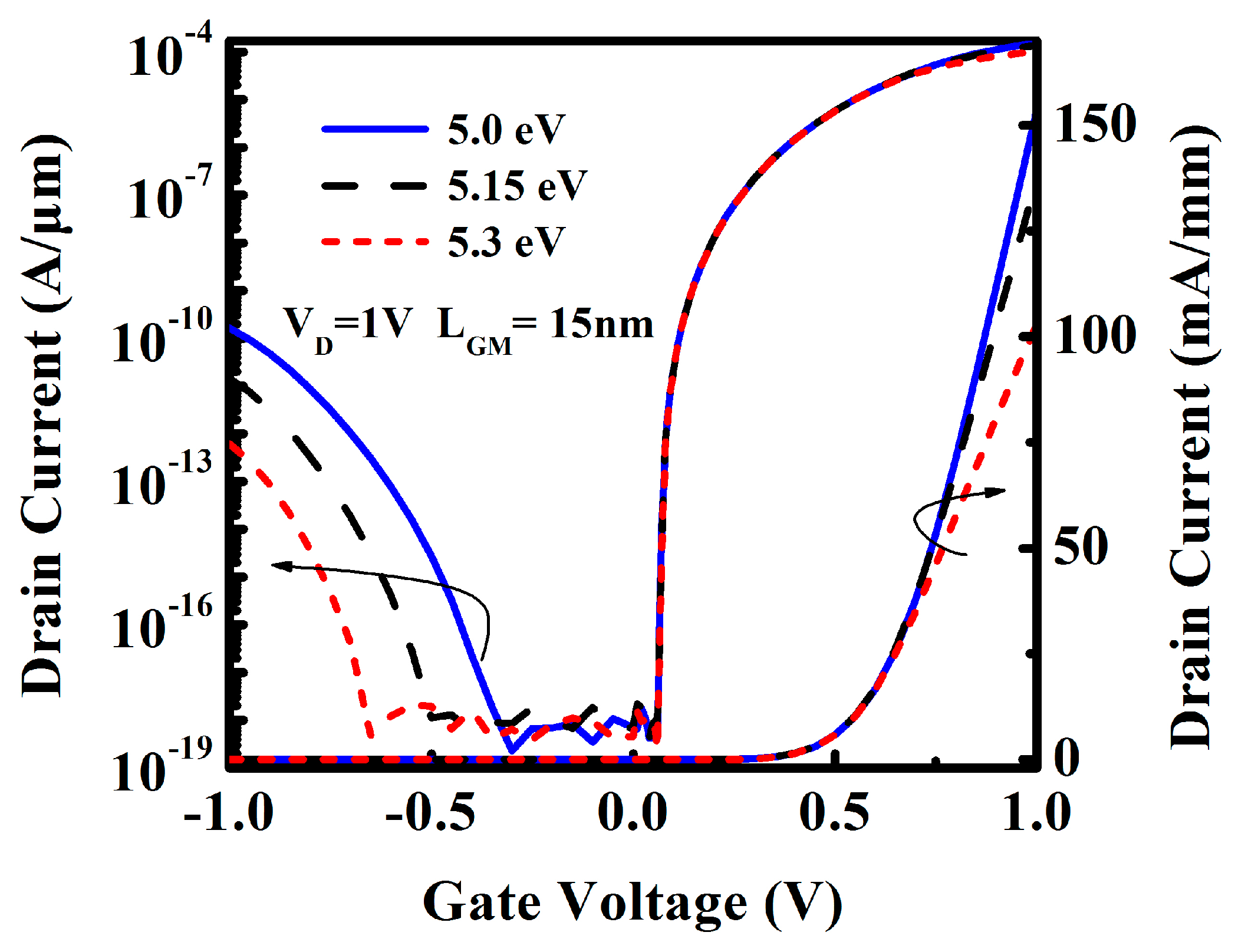
In this section, in order to find the optimal drain engineering metal, the impacts of the various of workfunction are studied in detail. The function of the drain engineering metal is to increase the tunneling barrier of the drain/channel junction at the negative VG bias, so a relatively high work function of the drain engineering metal may be a good choice. Here, electrical characteristics of DE-HTFET with drain engineering metal φM = 5.0, 5.15, and 5.3 eV are simulated, respectively, and the results are shown in Figure 4. Based on the results, it is indicated that Iambipolar presents an exponential decrease trend with the increment of φM, and ION stays in the same level. However, there is also a balance between Iambipolar and ION, that is to say, a higher workfunction is not always better. ION also reduces with the increment of φM, although it is in the same level. As φM increases from 5.0 eV to 5.15 eV, ION decreases slightly. However, at φM of 5.3 eV, ION decreases significantly, which is not desirable.
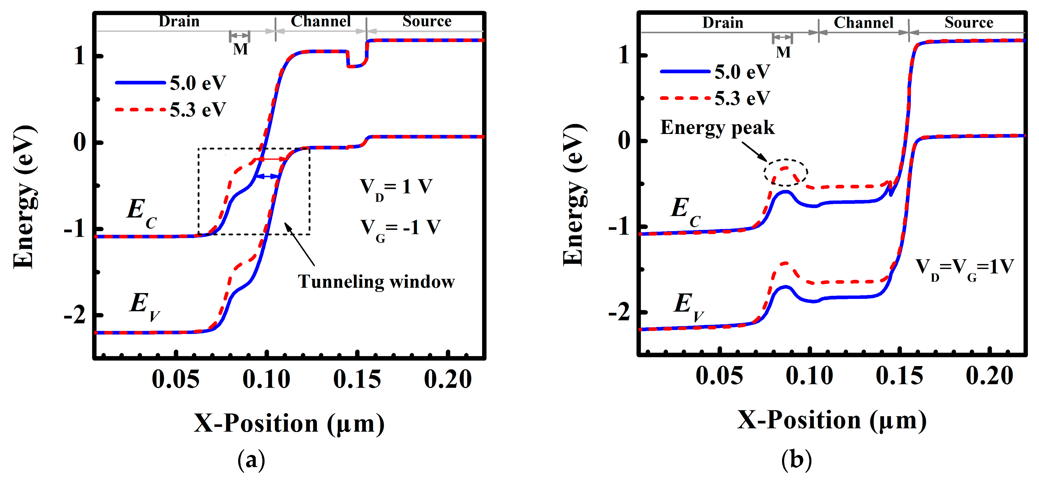
To gain a better insight into the variation of Iambipolar and ION, Figure 5 exhibits the energy band diagram of DE-HTFET with φM = 5.0 eV and 5.3 eV for VG of −1 V and 1 V, respectively. Figure 5a shows that the tunneling distance in the tunneling window for DE-HTFET with φM = 5.3 eV is larger than that for DE-HTFET with φM = 5.0 eV, which results in the lower BTBT tunneling rate at the drain/channel interface for DE-HTFET with higher φM, therefore, lower Iambipolar is obtained for higher φM. Figure 5b shows the energy band profile at the ON-state. An energy peak is created near the drain/channel interface, which will act as a barrier for electrons tunneling from the source to the drain region at the positive bias [28]. Therefore, ION of DE-HTFET with φM = 5.3 eV significantly degrades as shown in Figure 4. To make a trade-off between Iambipolar and ION, φM of 5.15 eV is selected as the last choice.
3.2. Polar Heterostructure DE-HTFET to Improve Device Performances
The heterostructures in TFETs studied above are all along the nonpolar plane, so no polarization charge exists at the interface of heterojunction. However, studies show that the polarization engineering in the III-nitride heterostructure can further adjust the energy band structure and achieve the interband tunneling [21]. It needs the heterostructure growing along the c-axis. Because of spontaneous polarization and piezoelectric polarization along the c-axis, large amounts of fixed polarization charge can be induced at the heterojunction interface. The polarization charge generated by polarization engineering can lead to a large internal electric field near the heterojunction interface, and increase the tunneling rate. On the other hand, polarization also changes the energy structure near the tunneling junction and helps improve TFET performance.
Herein, the polar and non-polar DE-HTFETs are compared. Figure 1c shows the schematic diagram of polar DE-HTFETs. The growth direction is along [0001], that is, the negative direction of X-axis in Figure 1. In this case, the polarization charge at the interface of III-Nitride heterojunction will be taken into account in the simulations. In particular, the polarization charge near the tunneling junction may have important effects on the device characteristics of InGaN DE-HTFET. By calculation, the density of polarization surface charge (σpol) is −1.27134 × 10¹³/cm2 at the position of TJ, and 1.27134 × 10¹³/cm2 at the position of HJ. The negative value of σpol represents a negative polarization charge, and vice versa.
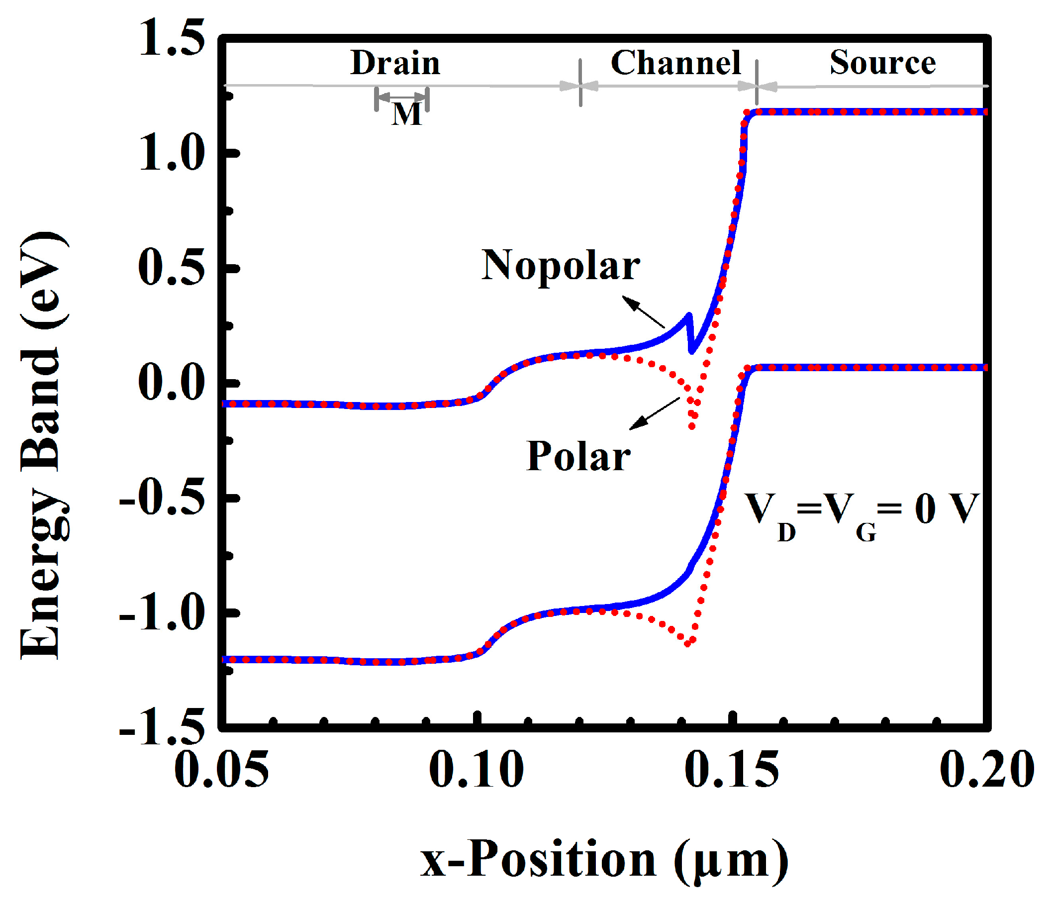
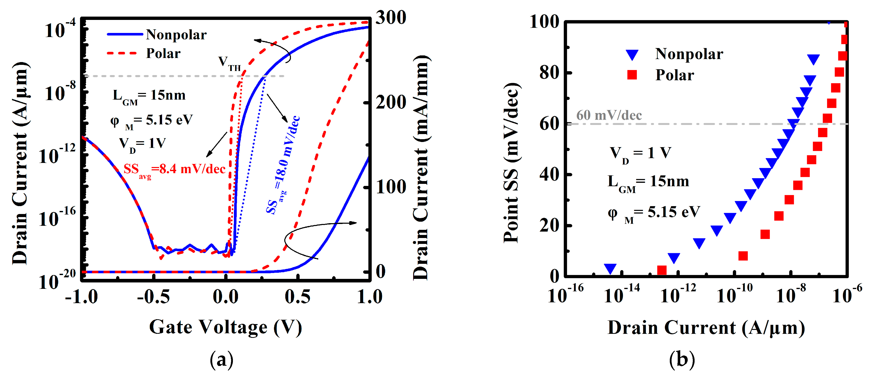
The polarization changes the energy structure near the tunneling junction. Figure 6 shows that the polar DE-HTFET has a steeper energy band near the tunneling junction, which facilitates the better subthreshold and ON-state characteristics. Figure 7a displays the transfer characteristic of nonpolar and polar DE-HTFETs at LGM of 15 nm and VD of 1 V. ID-VG curve indicates a smaller threshold voltage for the polar DE-HTFET, which will be more beneficial to the low-power applications. Besides this, the average subthreshold swing (SSavg) of the polar DE-HTFET is reduced by 53.3% compared to that of the nonpolar DE-HTFET. Also, ION increases 100% from 137 mA/mm of nonpolar DE-HTFET to 274 mA/mm of polar DE-HTFET. Figure 7b shows the point subthreshold swing (SSpoint) of TFETs with different ID extracted from the ID-VG curve. Obviously, SSpoint of the polar DE-HTFET is smaller than that of the nonpolar TFET at any ID value.
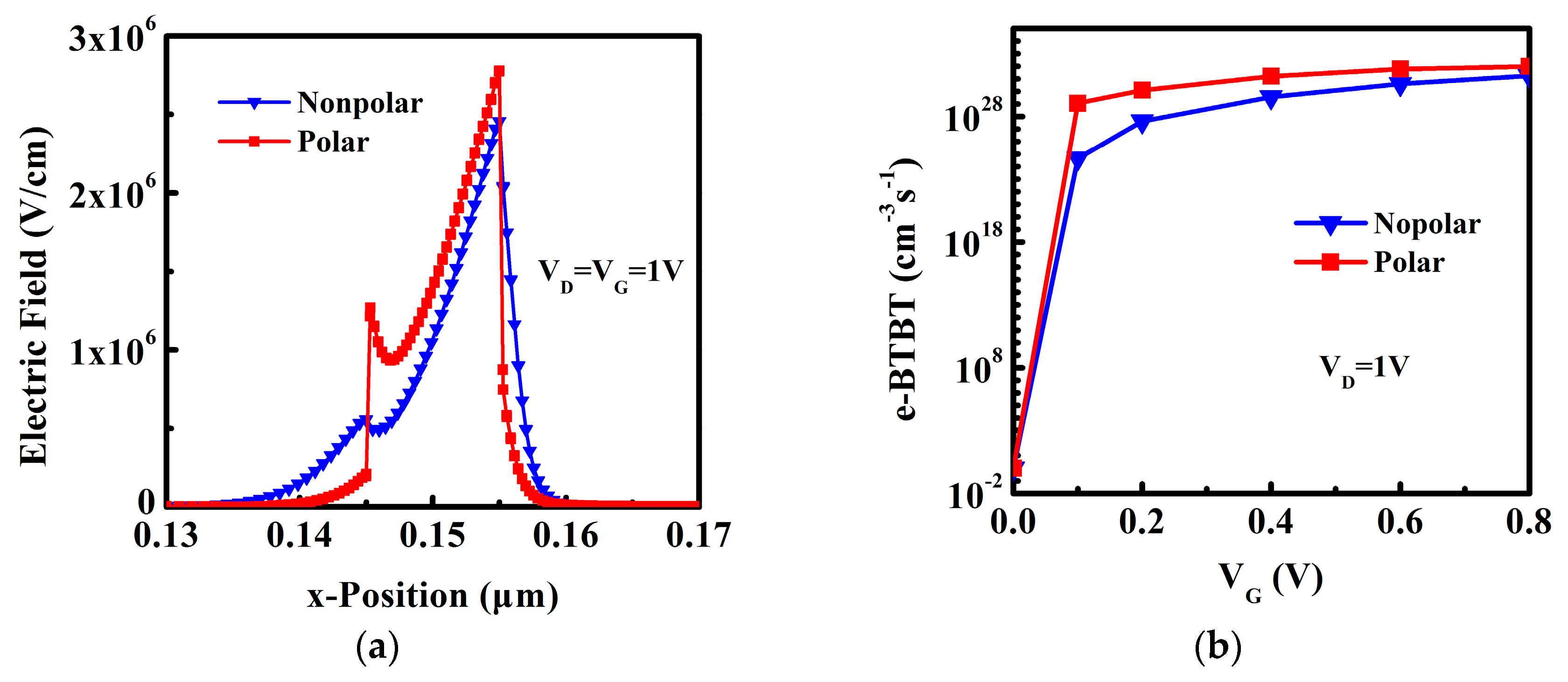
To further investigate the mechanism of performance improvement for polar DE-HTFET, the electric field and e-BTBT rate are discussed as follows. Figure 8a exhibits that the transverse electric field intensity of the channel near the tunneling junction of polar DE-HTFET is higher than that of the non-polar device under the effect of polarization at the ON-state. Therefore, the e-BTBT rate at ON-state between the source and channel of the polar DE-HTFET is much larger than that of the nonpolar DE-HTFET as shown in Figure 7b, which is consistent with Kane’s Formula (1). This is the reason why the polar InGaN DE-HTFETs have the larger ION. On the other hand, the e-BTBT rate with various of VG is shown in Figure 8b. When VG = 0 V, the tunneling rate of both TFETs is almost 0; when VG increases to 0.1 V, the tunneling rate of polar DE-HTFET increases to 1.14 × 1029 cm−3s−1, however the tunneling rate of non-polar DE-HTFET is only 4.49 × 1024 cm−3s−1. The significant increase of the tunneling rate with the increase of VG for polar DE-HTFETs in the subthreshold region makes polar DE-HTFETs have the lower subthreshold swing.
4. Conclusions
In summary, a drain engineered InGaN HTFET is investigated by Atlas simulation in this paper. Firstly, with the trade-off between Iambipolar and ION, Iambipolar is reduced from 1.93 × 10⁻⁸ A/μm of DE-HTFET to 1.46 × 10⁻¹¹ A/μm of HTFET by studying the impact of the drain engineering metal position and workfunction on device performances. The decreased Iambipolar results from the energy band modulation by the drain engineering metal and workfunction near the drain/channel junction in the drain region. Secondly, the polarization effect induces a large internal electric field near the heterojunction interface, changes the energy structure near the tunneling junction, and helps improve TFET performance. SSavg of the polar InGaN DE-HTFET is 8.4 mV/dec, which is reduced by 53.3% compared to that of the nonpolar InGaN DE-HTFET. Also, ION increases 100% from 137 mA/mm of nonpolar DE-HTFET to 274 mA/mm of polar DE-HTFET. Therefore, the structure of polar InGaN DE-HTFET embodies much more promising in low power applications.
Author Contributions
X.D. provided the concept, designed the structures, performed the simulations, and wrote the manuscript; J.Z. (Jincheng Zhang) and Y.H. gave valuable suggestions on the manuscript; All authors discussed the results and approved the final manuscript.
Funding
This work was supported by the National Key Research and Development Program (Grant No. 2016YFB0400100) and the Fundamental Research Funds for the Central Universities (Grand No. JB181104).
Conflicts of Interest
The authors declare no conflict of interest.
References
- Ionescu, A.M.; Riel, H. Tunnel field effect transistors as energy efficient electronic switches. Nature 2011, 479, 329–337. [Google Scholar] [CrossRef] [PubMed]
- Avci, U.E.; Morris, D.H.; Young, I.A. Tunnel field-effect transistors: Prospects and challenges. J. Electron. Dev. Soc. 2015, 3, 88–95. [Google Scholar] [CrossRef]
- Koswatta, S.O.; Lundstrom, M.S.; Nikonov, D.E. Performance comparison between p-i-n tunneling transistors and conventional MOSFETs. IEEE Trans. Electron Devices 2007, 56, 456–465. [Google Scholar] [CrossRef]
- Luisier, M.; Klimeck, G. Performance comparisons of tunneling field-effect transistors made of InSb, Carbon, and GaSb–InAs broken gap heterostructures, In Proceedings of the IEEE International Electron Devices Meeting (IEDM), Baltimore, MD, USA, 7–9 December 2009; pp. 1–4. [Google Scholar]
- Nirschla, T.; Henzler, S.; Fischer, J.; Fulde, M.; Bargagli-Stoffi, A.; Sterkel, M.; Sedlmeir, J.; Weber, C.; Heinrich, R.; Schaper, U.; et al. Scaling properties of the tunneling field effect transistor (TFET): Device and circuit. Solid-State Electron. 2006, 50, 44–51. [Google Scholar] [CrossRef]
- Vijayvargiya, V.; Vishvakarma, S.K. Effect of drain doping profile on double-gate tunnel field-effect transistor and its influence on device RF performance. IEEE Trans. Nanotechnol. 2014, 13, 974–981. [Google Scholar] [CrossRef]
- Loan, S.A.; Alharbi, A.G.; Rafat, M. Ambipolar leakage suppression in electron–hole bilayer TFET: Investigation and analysis. J. Comput. Electron. 2018, 17, 977–985. [Google Scholar]
- Beneventi, G.B.; Gnani, E.; Gnudi, A.; Reggiani, S.; Baccarani, G. Dual-metal-gate InAs tunnel FET with enhanced turn-on steepness and high ON-current. IEEE Trans. Electron. Dev. 2014, 61, 776–784. [Google Scholar] [CrossRef]
- Choi, W.Y.; Lee, W. Hetero-gate-dielectric tunneling field-effect transistors. IEEE Trans. Electron. Dev. 2010, 57, 2317–2319. [Google Scholar] [CrossRef]
- Chauhan, S.S.; Sharma, N. Enhancing analog performance and suppression of subthreshold swing using hetero-junctionless double gate TFETs. Superlattices Microstruct. 2017, 112, 257–261. [Google Scholar] [CrossRef]
- Peng, Y.; Han, G.; Wang, H.; Zhang, C.; Liu, Y.; Wang, Y.; Zhao, S.; Zhang, J.; Hao, Y. InN/InGaN complementary heterojunction-enhanced tunneling field-effect transistor with enhanced subthreshold swing and tunneling current. Superlattices Microstruct. 2016, 93, 144–152. [Google Scholar] [CrossRef]
- Wang, H.; Liu, Y.; Liu, M.; Zhang, Q.; Zhang, C.; Ma, X.; Zhang, J.; Hao, Y.; Han, G. Performance improvement in novel germanium–tin/germanium heterojunction-enhanced p-channel tunneling field-effect transistor. Superlattices Microstruct. 2015, 83, 401–410. [Google Scholar] [CrossRef]
- Wang, Y.; Liu, Y.; Han, G.; Wang, H.; Zhang, C.; Zhang, J.; Hao, Y. Theoretical investigation of GaAsBi/GaAsN tunneling field-effect transistors with type-II staggered tunneling junction. Superlattices Microstruct. 2017, 106, 139–146. [Google Scholar] [CrossRef]
- Raad, B.R.; Sharma, D.; Kondekar, P.; Nigam, K.; Baronia, S. DC and analog/RF performance optimisation of source pocket dual work function TFET. Int. J. Electron. 2017, 104, 1992–2006. [Google Scholar] [CrossRef]
- Chang, H.-Y.; Adams, B.; Chien, P.-Y.; Li, J.; Woo, J.C.S. Improved subthreshold and output characteristics of source-pocket Si tunnel FET by the application of laser annealing. IEEE Trans. Electron Devices 2013, 60, 92–96. [Google Scholar] [CrossRef]
- Kumar, M.J.; Janardhanan, S. Doping-less tunnel field effect transistor: Design and investigation. IEEE Trans. Electron Devices 2013, 60, 3285–3290. [Google Scholar] [CrossRef]
- Bashir, F.; Loan, S.A.; Rafat, M.; Alamoud, A.R.M.; Abbasi, S.A. A high performance gate engineered charge plasma based tunnel field effect transistor. J. Comput. Electron. 2015, 14, 477–485. [Google Scholar] [CrossRef]
- Duan, X.; Zhang, J.; Wang, S.; Li, Y.; Xu, S.; Hao, Y. A High-Performance Gate Engineered InGaN Dopingless Tunnel FET. IEEE Trans. Electron Devices 2018, 65, 1223–1229. [Google Scholar] [CrossRef]
- Abdi, D.B.; Kumar, M.J. PNPN tunnel FET with controllable drain side tunnel barrier width: Proposal and analysis. Superlattices Microstruct. 2015, 86, 121–125. [Google Scholar] [CrossRef]
- Sahay, S.; Kumar, M.J. Controlling the drain side tunneling width to reduce ambipolar current in tunnel FETs using heterodielectric BOX. IEEE Trans. Electrons Devices 2015, 62, 3882–3885. [Google Scholar] [CrossRef]
- Li, W.; Sharmin, S.; Ilatikhameneh, H.; Rahman, R.; Lu, Y.; Wang, J.; Yan, X.; Seabaugh, A.; Klimeck, G.; Jena, D.; et al. Polarization-Engineered III-Nitride Heterojunction Tunnel Field-Effect Transistors. IEEE J. Explor. Solid-State Comput. Devices Circuits 2015, 1, 28–34. [Google Scholar] [CrossRef]
- Li, W.; Cao, L.; Lund, C.; Keller, S.; Fay, P. Performance projection of III-nitride heterojunction nanowire tunneling field-effect transistors. Phys. Status Solidi A 2016, 213, 905–908. [Google Scholar] [CrossRef]
- Cho, M.S.; Kwon, R.H.; Seo, J.H.; Yoon, Y.J.; Jang, Y.I.; Won, C.H.; Kim, J.-G.; Lee, J.; Cho, S.; Lee, J.-H.; et al. Electrical performances of InN/GaN tunneling field-effect transistor. J. Nanosci. Nanotechnol. 2017, 17, 8355–8359. [Google Scholar] [CrossRef]
- Duan, X.; Zhang, J.; Wang, S.; Quan, R.; Hao, Y. Effect of graded InGaN drain region and ‘In’ fraction in InGaN channel on performances of InGaN tunnel field-effect transistor. Superlattices Microstruct. 2017, 112, 671–679. [Google Scholar] [CrossRef]
- ATLAS Device Simulation Software, Silvaco Int.: Santa Clara, CA, USA, 2013.
- Duan, X.; Zhang, J.; Xiao, M.; Zhao, Y.; Ning, J.; Hao, Y. Groove-type channel enhancement-mode AlGaN/GaN MIS HEMT with combined polar and nonpolar AlGaN/GaN heterostructures. Chin. Phys. B 2016, 25, 087304. [Google Scholar] [CrossRef]
- Verhulst, A.S.; Vandenberghe, W.G.; Maex, K.; Groeseneken, G. Boosting the on-current of a n-channel nanowire tunnel field-effect transistor by source material optimization. J. Appl. Phys. 2008, 104, 064514. [Google Scholar] [CrossRef]
- Raad, B.R.; Sharma, D.; Kondekar, P.; Nigam, K.; Yadav, D.S. Drain work function engineered doping-less charge plasma TFET for ambipolar suppression and RF performance improvement: A proposal, design, and investigation. IEEE Trans. Electron Devices 2016, 63, 3950–3957. [Google Scholar] [CrossRef]
Figure 1.
Cross-sectional views of the nonpolar (a) conventional, (b) drain engineered InGaN tunnel field effect transistor (TFET), and (c) polar drain engineered InGaN TFET.
Figure 1.
Cross-sectional views of the nonpolar (a) conventional, (b) drain engineered InGaN tunnel field effect transistor (TFET), and (c) polar drain engineered InGaN TFET.

Figure 2.
(a) Transfer characteristic of HTFET and DE-HTFET with varied LGM at VD of 1 V and φM of 5.15 eV, and (b) ambipolar current with different LGM extracted from the I-V curve.
Figure 2.
(a) Transfer characteristic of HTFET and DE-HTFET with varied LGM at VD of 1 V and φM of 5.15 eV, and (b) ambipolar current with different LGM extracted from the I-V curve.

Figure 3.
(a) Energy band diagram of DE-HTFET near the drain/channel tunneling junction with LGM = 15 nm at VG of −1 V, VD of 1 V, and (b) Energy band diagram of DE-HTFET at ON-state.
Figure 3.
(a) Energy band diagram of DE-HTFET near the drain/channel tunneling junction with LGM = 15 nm at VG of −1 V, VD of 1 V, and (b) Energy band diagram of DE-HTFET at ON-state.

Figure 4.
Transfer characteristic of DE-HTFET with various φM at VD of 1 V.

Figure 5.
Energy band diagram at the line 1 nm away from the interface of InGaN/Al2O3 for DE-HTFET with φM = 5.0 eV and 5.3 eV as (a) VD = 1 V, VG = −1 V, and (b) VD = VG = 1 V.
Figure 5.
Energy band diagram at the line 1 nm away from the interface of InGaN/Al2O3 for DE-HTFET with φM = 5.0 eV and 5.3 eV as (a) VD = 1 V, VG = −1 V, and (b) VD = VG = 1 V.

Figure 6.
Energy band diagram in the thermal state.

Figure 7.
(a) Transfer characteristic and (b) point subthreshold swing for the nonpolar and polar InGaN TFET at VD of 1 V.
Figure 7.
(a) Transfer characteristic and (b) point subthreshold swing for the nonpolar and polar InGaN TFET at VD of 1 V.

Figure 8.
(a) Electric field in the ON-state, and (b) electron tunneling rate with various VG.


Table 1.
Material parameters used in simulations [21].
Table 1.
Material parameters used in simulations [21].
| Parameters | In0.75Ga0.25N | In0.85Ga0.15N |
|---|---|---|
| Band gap Eg (eV) | 1.1125 | 0.9265 |
| Hole effective mass (m0) | 0.295 | 0.273 |
| Electron effective mass (m0) | 0.1025 | 0.0895 |
| Static dielectric constant εr | 12.75 | 13.05 |
| Electron mobility μe (cm2/Vs) | 1050 | 1050 |
| Hole mobility μh (cm2/Vs) | 20 | 20 |
© 2019 by the authors. Licensee MDPI, Basel, Switzerland. This article is an open access article distributed under the terms and conditions of the Creative Commons Attribution (CC BY) license (http://creativecommons.org/licenses/by/4.0/).
Share and Cite
MDPI and ACS Style
Duan, X.; Zhang, J.; Chen, J.; Zhang, T.; Zhu, J.; Lin, Z.; Hao, Y. High Performance Drain Engineered InGaN Heterostructure Tunnel Field Effect Transistor. Micromachines 2019, 10, 75. https://doi.org/10.3390/mi10010075
AMA Style
Duan X, Zhang J, Chen J, Zhang T, Zhu J, Lin Z, Hao Y. High Performance Drain Engineered InGaN Heterostructure Tunnel Field Effect Transistor. Micromachines. 2019; 10(1):75. https://doi.org/10.3390/mi10010075
Chicago/Turabian StyleDuan, Xiaoling, Jincheng Zhang, Jiabo Chen, Tao Zhang, Jiaduo Zhu, Zhiyu Lin, and Yue Hao. 2019. "High Performance Drain Engineered InGaN Heterostructure Tunnel Field Effect Transistor" Micromachines 10, no. 1: 75. https://doi.org/10.3390/mi10010075
Note that from the first issue of 2016, this journal uses article numbers instead of page numbers. See further details here.