Compensating Circuit to Reduce the Impact of Wire Resistance in a Memristor Crossbar-Based Perceptron Neural Network


Faculty of Electrical and Electronics Engineering, Ho Chi Minh City University of Technology and Education, Ho Chi Minh City 70000, Vietnam
Micromachines 2019, 10(10), 671; https://doi.org/10.3390/mi10100671
Submission received: 23 September 2019
/
Revised: 23 September 2019
/
Accepted: 1 October 2019
/
Published: 2 October 2019
(This article belongs to the Special Issue Emerging Memory and Computing Devices in the Era of Intelligent Machines)
Abstract
:Wire resistance in metal wire is one of the factors that degrade the performance of memristor crossbar circuits. In this paper, an analysis of the impact of wire resistance in a memristor crossbar is performed and a compensating circuit is proposed to reduce the impact of wire resistance in a memristor crossbar-based perceptron neural network. The goal of the analysis is to figure out how wire resistance influences the output voltage of a memristor crossbar. It emerges that the wire resistance on horizontal lines causes the neuron’s output voltage to vary more than the wire resistance on vertical lines. More interesting, the voltage variation caused by wire resistance on horizontal lines increases proportionally to the length of metal wire. The first column has small voltage variation whereas the last column has large voltage variation. In addition, two adjacent columns have almost the same amount of voltage variation. Under these observations, a memristor crossbar-based perceptron neural network with compensating circuit is proposed. The neuron’s outputs of two columns are put into a subtractor circuit to eliminate the voltage variation caused by the wire resistance. The proposed memristor crossbar-based perceptron neural network is trained to recognize the 26 characters. The proposed memristor crossbar shows better recognition rate compared to the previous work when wire resistance is taken into account. The proposed memristor crossbar circuit can maintain the recognition rate as high as 100% when wire resistance is as high as 2.5 Ω. By contrast, the recognition rate of the memristor crossbar without the compensating circuit decreases by 1%, 5%, and 19% when wire resistance is set to be 1.5, 2.0, and 2.5 Ω, respectively.
1. Introduction
Neuromorphic computing, inspired from biological perception, was introduced by C. Mead in the late 1980s [1]. It has been expected to become an alternative architecture to overcome the bottleneck of von Neumann computer architectures [1,2]. Neuromorphic computing refers to a hardware implementation of a brain-inspired system, which has the capabilities of parallel processing like a human brain. For realizing neuromorphic computing systems, various research activities, based on CPUs (Central Processing Units), GPUs (Graphics Processing Units), FPGAs (Field-Programmable Gate Arrays), analog circuits, memory circuits, etc., have been proposed in the past two decades [3,4,5,6,7,8]. These architectures are based on CMOS (Complementary-Metal-Oxide-Semiconductor) technology, which is approaching the end of their capabilities because scaling CMOS down faces several fundamental limiting factors stemming from electron thermal energy and quantum-mechanical tunneling [9,10]. The memristor crossbar array has been one of the promising candidates for realizing neuromorphic computing systems because crossbar architecture can be made with high density and low cost [11]. Memristor was postulated by Leon O. Chua in 1971 as the fourth basic circuit element and experimentally demonstrated by HP Lab in 2008 [12,13]. A memristor is a resistor with modifiable resistance, which makes it ideal for mimicking the synaptic plasticity of biological neurons [14]. The early memristor-based synaptic circuits are composed of memristors and CMOS transistors [15,16,17]. However, pure memristor crossbar arrays without CMOS devices seem to be more efficient in terms of their integration and power consumption [18,19,20,21,22,23]. Miao Hu et al. proposed a crossbar synaptic array that is composed of a plus and minus crossbar array representing plus- and minus-polarity connection matrices for analog neuromorphic computing [20]. Such a pure memristor crossbar array is very effective in realizing the bio-inspired systems in term of power consumption and area occupation. To reduce area and power consumption, S. N. Truong proposed a new memristor crossbar array architecture which is composed of a single memristor array and a constant-term circuit [21].
In a memristor array, some amount of voltage drop can be caused by interconnect resistance, also known as wire resistance along the row and the column lines [19,24,25,26,27]. Wire resistance degrades the performance of the circuit more seriously when the array size increases [25]. To mitigate the impact of wire resistance, several interesting schemes were proposed [24,25,26,27]. These schemes are effective when they are applied to a memristor crossbar array, in which memristors are used as binary switches between two distinct high and low resistance states (HRS and LRS, respectively). However, the impact of wire resistance in an analog memristor crossbar array for realizing the synaptic weight matrix was not fully considered. In this work, we propose a memristor crossbar array with a compensating circuit for implementing the analog synaptic array of a perceptron neural network. The impact of wire resistance is mitigated by compensating the voltage variation of two adjacent columns.
In this work, the output voltages of columns are figured out with taking the existing of wire resistance into account. The mathematical analysis and the simulation result show that the output voltage of columns increase, which is caused by the amount of voltage lost from wire resistance. The column close to the first one has a small variation of voltage, compared to the one far from the first column. From these observations, we propose a compensating circuit to mitigate the voltage variation caused by the wire resistance in a memristor crossbar array.
2. Materials and Methods
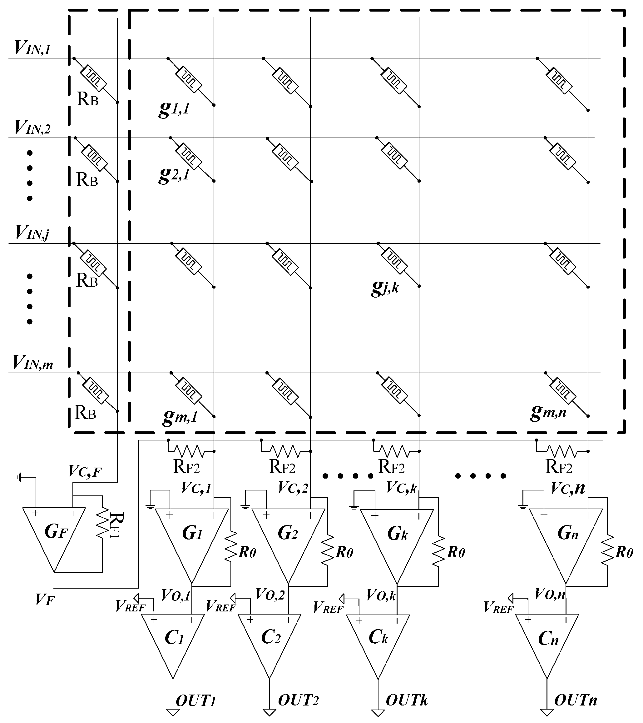
Figure 1 shows an interesting memristor array circuit for implementing the synaptic weight matrix of a perceptron neural network [21]. A single memristor array and a constant-term circuit are used for realizing the negative and positive synaptic weights, instead of using two complementary crossbar arrays [20,21].
In Figure 1, is the memristor’s conductance at the crossing point between the jth row and the kth column. VIN,j is the input voltage applied to the jth row. VC,k is the column-line voltage on the kth column. The column line, VC,F, is added in Figure 1 instead of using another memristor array [21]. The column line, VC,F, is connected to the inputs, from VIN,1 to VIN,m. In Figure 1, VC,F enters GF that constitutes an inverting OP amp with the negative feedback resistor, RF1. The output voltage of GF is VF that is connected to all the column lines from VC,1 to VC,n via RF2, as shown in Figure 1. By applying Kirchhoff current law to the column line, VC,F, we can calculate VF and VO,k with Equations (1) and (2).
If we choose RF1 = RF2 and combining Equation (1) with Equation (2), the following Equation (3) can be obtained [21].
If is defined as a synaptic weight of the jth row and kth column, wj,k, we can rewrite Equation (3) with Equation (4).
where .
Equation (4) is used for calculating the output voltage of the kth column. The output of each column is a summation of the weighted inputs, hence each column works as a perceptron neuron. In Equation (4), Mj,k is the memristance value of the crossing point between the jth row and kth column. RB is a constant. The synaptic weight, wj,k, can be decided to be either negative or positive by adjusting the memristance, Mj,k. The output of the perceptron neuron is decided by a threshold function which produces 0 or 1. By adding the comparator to the output voltage, VO,k, we can decide if the neuron’s output of the kth column, OUTk, should be activated or not.
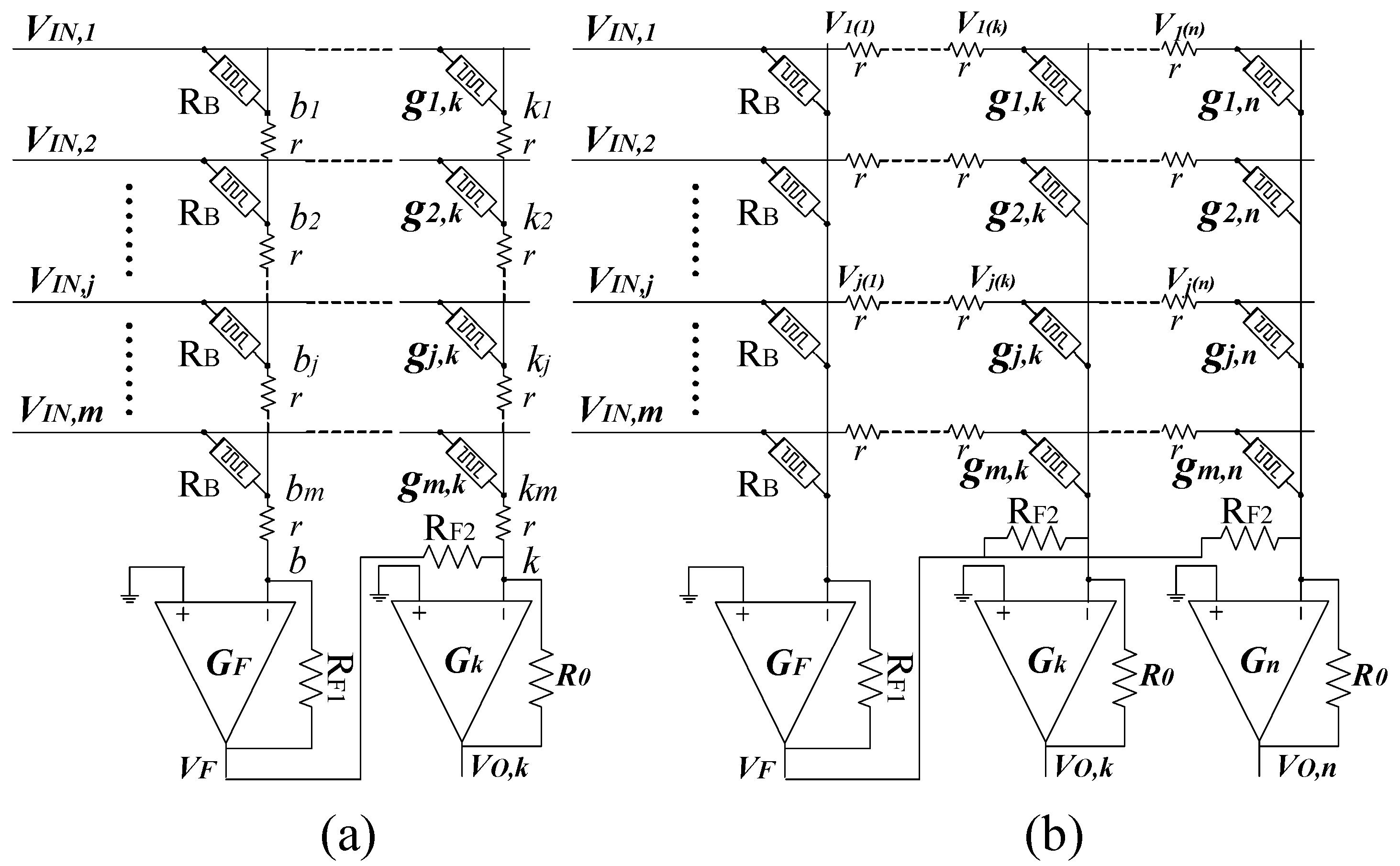
In previous work, the impact of wire resistance is ignored. However, in the crossbar array, the voltage drop along column and row lines cannot be omitted [19,24,25,26,27]. It becomes more serious when the array size increases [24]. The wire resistance between two adjacent junctions is modeled by a small-value resistor, r, as shown in Figure 2.
For the sake of simplicity, in this section we analyze the circuit separately with respect to the wire resistance on horizontal lines and the wire resistance on vertical lines, as shown in Figure 2a,b, respectively. We define Vb1, Vb2 as the voltages of node b1, b2, which are on the first column. Generally, Vbj is the voltage of node bj on the first column. Similarly, Vkj is the voltage of node kj, which is on the jth column. Applying Kirchhoff current law for all nodes in Figure 2a, VF and VO,k can be estimated as follows:
If we assume that RF1 = RF2, Equation (7) can be simplified as follow:
By comparing Equation (8) and Equation (4), we can derive the variation of voltage, ∆V, which is caused by wire resistance on the vertical lines.
Here Mj,k is the memristance of the crossing point between the jth row and the kth column. Vbj and Vkj are the voltage at nodes bj and kj of the first column and the kth column, respectively, as shown in Figure 2a. Mj,k is calculated using Equation (4). It is possible to infer that the variation of voltage presented in Equation (9) can be very small because there are a negative term and a positive term in the right side of Equation (9).
In Figure 2b, wire resistance on vertical lines is omitted whereas wire resistance on horizontal lines is taken into account. The voltages applied to the columns decrease because they are lost from wire resistance. If we define Vj(k) as the amount of voltage drop on wire resistance, which is on the jth row and between the (k − 1)th and kth column, the voltage applied to the jth row of the kth column is calculated as Equation (10).
Here VIN,j(k) is the voltage applied to the jth row of the kth column. The column-line voltage on the kth column, VO,k, can be calculated using Equation (11).
By comparing Equation (11) and Equation (3), we obtain the variation of voltage, ∆Vk, of the kth column as follows.
Calculating VIN,j(k) by using Equation (10), we obtain ∆Vk as presented in Equation (13).
Here is the sum of the voltage on k resistors on the jth row. Equation (13) indicates that the output voltage of the kth column increases because of wire resistance. It is possible to infer that the column close to the first column has small voltage variation and the column far from the first column has large voltage variation. In Equation (13), the voltage variation increases proportionally to the column’s index, k. Hence, it is interesting that two adjacent columns can have almost the same amount of voltage variation. Due to this reason, we propose a memristor crossbar array with compensating circuit to mitigate the voltage variation caused by wire resistance. By putting two adjacent columns into a subtraction circuit, the voltage variation can be eliminated significantly. The proposed memristor crossbar is schematically shown in Figure 3.
In Figure 3, the memristor crossbar is composed of 27 columns for recognizing 26 character images. The first column is a constant-term circuit to generate a negative voltage, as mentioned in the previous section. The remaining 26 columns represent 26 perception neurons trained to recognize the 26 characters. The differential amplifies from Gs,2 to Gs,26 are inserted into the circuit. The gain of these amplifiers is 1, so they work as the subtractors. The output voltages from VO,1 to VO,n are the neuron’s output of columns from Col1 to Coln. VO,1 enter the comparator C1 to decide if the neuron’s output of column Col1 should be activated or not. VO,2 and VO,1 go into Gs,2 that produces VOs,2. VOs,2 enters the comparator C2 to decide if the neuron’s output of column Col2 should be activated or not. In general, the output voltage of the column Colk−1 and the column Colk enter the subtractor Gs,k for generating the neuron’s output, VOs,k, of the column Colk. Using superposition theorem, VOs,k can be calculated with the difference of VO,k − 1 and VO,k.
If we assume that R3 = R4 = R5 = R6, we can obtain:
The differential amplifier is able to reject any signal common to both inputs. That means, if two adjacent columns have almost the same amount of voltage variation, the voltage variation is then mitigated at the output.
The concept of the proposed circuit is shown in Figure 4. The crossbar is trained to recognize the 26 characters from “A” to “Z”. The 25th column is for recognizing the character “Y”. The output of the 25th column is close to 1V when the input is “Y” and close to 0 when the other characters are applied to the input. Similarly, the neuron’s output of the 26th column should be activated if the input is “Z”, as indicated in Figure 4a. In Figure 4b, it is assumed that the wire resistance is present in the crossbar. The output voltage increases as reasoned in the previous section. The two last neurons recognize the input characters incorrectly, as demonstrated in Figure 4b. However, if we put the outputs of two last columns into a subtractor, the voltage variation can be mitigated significantly, as illustrated in Figure 4b. By doing this, we can maintain the recognition rate when wire resistance is present in the crossbar circuit.
3. Results
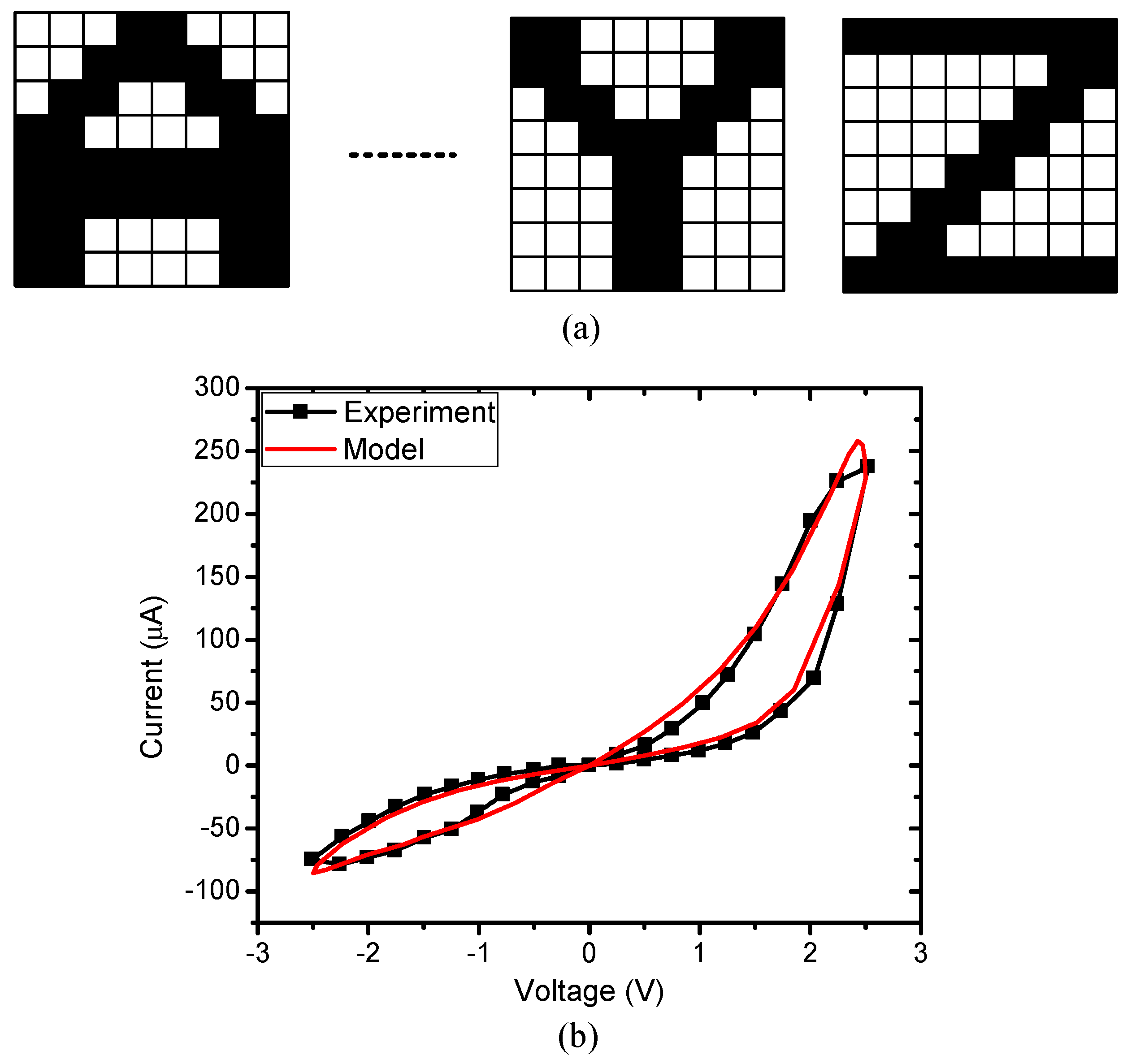
The proposed memristor crossbar circuit in Figure 3 is verified for the application of character recognition. Figure 5a shows eight × eight images of characters used in this simulation. Each character is composed of 64 black-and-white pixels. The proposed memristor crossbar is composed of 64 rows and 27 columns. The first column connects with all inputs through RB to generate the negative voltage as mentioned in the previous section. The remaining 26 columns are for recognition of 26 characters from “A” to “Z”. The 64 input voltages obtained from 64 pixels are applied to the inputs of 64 rows.
The red line in Figure 5b shows a hysteresis behavior of a real memristor based on the film structure of Pt/LaAlO3/Nb-doped SrTiO3 stacked layer [28]. The black line in Figure 5b represents the behavior model of the memristor used in this paper. This model can well describe various memristive behaviors that come from different kinds of memristors [29]. The circuit simulation is performed using the SPECTRE circuit simulation provided by Cadence Design Systems Inc. Memristors are modeled using Verilog-A and the CMOS technology is given by SAMSUNG 0.13 mm process technology [29,30]. The Verilog-A model parameters are presented in [28]. The wire resistance between two adjacent junctions is set to be 2.5 Ω for a 4F2 cross-point structure [19,31]. Figure 6a shows the neuron’s output of the 25th column, which is trained to be activated when character “Y” is applied to the input. Ideally, VO,25 is close to 1V for character “Y”, and close to 0V for others. However, the output voltage of the 25th column, VO,25, is shifted up because of wire resistance, as reasoned in the previous section. Similarly, in Figure 6b, the neuron’s output of the 26th column is shifted up as a result of the voltage drop along wire resistance. It can be realized that if we compare the column’s output voltage, VO,26, with the reference voltage, VREF, the neuron’s output of the 26th column can be activated for several input characters, which consequently degrades the recognition rate. The output voltage of the 25th column and the 26th column are put into a subtractor circuit to produce the neuron’s output voltage of the 26th column, VOs,26. By doing this, the voltage variation is mitigated significantly, as demonstrated in Figure 6c. When the character “Y” is applied to the inputs, VOs,26 is negative, because VO,25 is higher than VO,26. For the character “Z”, VOs,26 is high, as indicated in Figure 6c. The simulation result shown in Figure 6c indicates that the neuron’s output of the 26th column is only activated for the input character “Z”, because the variation of voltage caused by wire resistance is mitigated remarkably by the subtractor circuit.
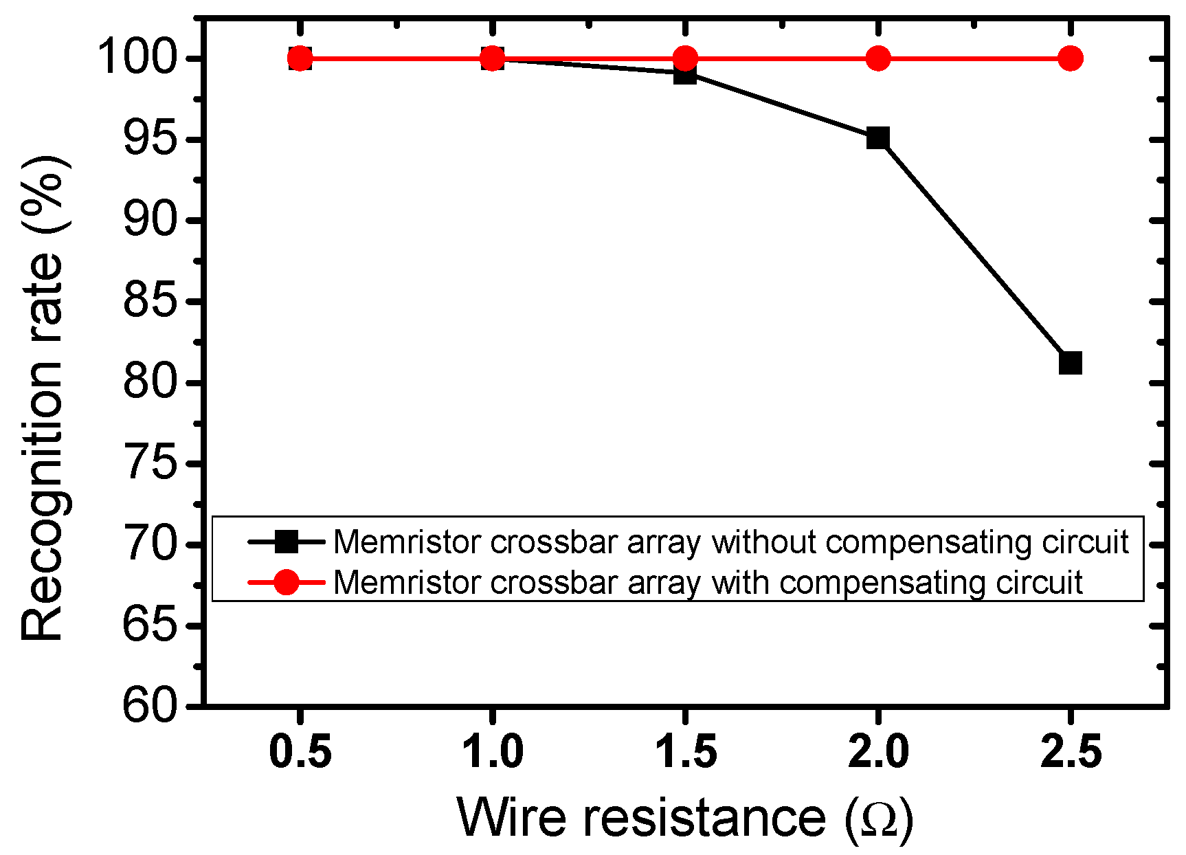
The proposed circuit is tested with wire resistance that is varied from 0.5 to 2.5 Ω. This range of wire resistance is commonly used and obtained from the International Technology Roadmap for Semiconductors [24,25,31,32,33,34]. Figure 7 shows the comparison of the recognition rate between the memristor crossbar without compensating circuit and the proposed memristor crossbar with compensating circuit when the wire resistance is set to be 0.5, 1.0, 1.5, 2.0, and 2.5 Ω, respectively. The recognition rate of the memristor crossbar without compensating circuit declines dramatically when wire resistance increases. In particular, the recognition rate of the memristor crossbar without compensating circuit is 99%, 95%, and 81%, when the wire resistance is set to be 1.5, 2.0, and 2.5 Ω, respectively. By contrast, the proposed memristor crossbar with compensating circuit can maintain the recognition as high as 100% when wire resistance is as high as 2.5 Ω.
4. Discussion
Finally, we discuss the power and area overhead of the proposed memristor crossbar circuit. The proposed circuit uses the compensating circuit constituted by an Op-Amp and four resistors. The proposed circuit consumes more power and area, compared to the memristor crossbar without compensating circuit. However, the proposed memristor crossbar with compensating circuit shows better recognition rate by 19% than the previous memristor crossbar circuit, when wire resistance is set to be 2.5 Ω. Because wire resistance in the crossbar cannot be omitted, the proposed scheme makes the memristor crossbar-based perceptron neural network become more possible. The proposed circuit can be applied to memristor-based crossbar architectures which are used in resistive memory and artificial neural networks [34,35,36].
5. Conclusions
In this work, a memristor crossbar-based perceptron neural network with compensating circuit is proposed. The neuron’s outputs of two columns are put into a subtractor circuit to eliminate the voltage variation caused by wire resistance. The memristor crossbar-based perceptron neural network is trained to recognize the 26 characters. The proposed memristor crossbar with compensating circuit shows better recognition rate, compared to the previous memristor crossbar without compensating circuit when wire resistance is taken into account. The simulation result shows that the proposed circuit can maintain the recognition rate as high as 100% when the wire resistance is set to be 2.5 Ω. By contrast, the recognition rate of the memristor crossbar without compensating circuit decreases by 19% when wire resistance is set to be 2.5 Ω.
Funding
This research received no external funding.
Conflicts of Interest
The author declares no conflicts of interest.
References
- Mead, C. Neuromorphic electronic systems. Proc. IEEE 1990, 78, 1629–1636. [Google Scholar] [CrossRef] [Green Version]
- Pacheco, P.S. An Introduction to Parallel Programmin; Elsevier: Amsterdam, The Netherlands, 2011. [Google Scholar]
- Mirsa, J.; Saha, I. Artificial neural networks in hardware: A survey of two decades of progress. Neurocomputing 2010, 74, 239–255. [Google Scholar]
- Himavathi, S.; Anitha, D.; Muthuramalingam, A. Feedforward neural network implementation in FPGA using layer multiplexing for effective resource utilization. IEEE Trans. Neural Netw. 2007, 18, 880–888. [Google Scholar] [CrossRef] [PubMed]
- Du, Y.; Du, L.; Gu, X.; Du, J.; Wang, X.S.; Hu, B.; Jiang, M.; Chen, X.; Su, J.; Iye, S.S.; et al. An analog neural network computing engine using CMOS-compatible charge-trap-transistor (CTT). IEEE Trans. Comput. Aided Des. Integr. Circuits Syst. 2018, 38, 1811–1819. [Google Scholar] [CrossRef]
- Kawaguchia, M.; Ishiib, N.; Umeno, M. Analog neural circuit and hardware design of deep learning model. Procedia Comput. Sci. 2015, 60, 976–985. [Google Scholar] [CrossRef]
- Wang, F.; Li, Y.X. Analog Circuit Design Automation Using Neural Network-Based Two-Level Genetic Programming. In Proceedings of the 2006 International Conference on Machine Learning and Cybernetics, Dalian, China, 13–16 August 2006. [Google Scholar]
- Shima, T.; Kimura, T.; Kamatani, Y.; Itakura, T.; Fujita, Y.; Iida, T. Neuro chips with on-chip back-propagation and/or Hebbian learning. IEEE J. Solid-State Circuits 1992, 27, 1868–1875. [Google Scholar] [CrossRef]
- Solomon, P.M. Device innovation and material challenges at the limit of CMOS technology. Annu. Rev. Mater. Sci. 2000, 30, 681–697. [Google Scholar] [CrossRef]
- Brđanin, T.P.; Dokić, B. Strained silicon layer in CMOS technology. Electronics 2014, 18, 63–69. [Google Scholar]
- Kügeler, C.; Meier, M.; Rosezin, R.; Gilles, S.; Waser, R. High density 3D memory architecture based on the resistive switching effect. Solid State Electron. 2009, 53, 1287–1292. [Google Scholar] [CrossRef]
- Chua, L.O. Memristor—The missing circuit element. IEEE Trans. Circuit Theory 1971, 18, 507–519. [Google Scholar] [CrossRef]
- Strukov, D.B.; Sinder, G.S.; Stewart, D.R.; Williams, R.S. The missing memristor found. Nature 2008, 453, 80–83. [Google Scholar] [CrossRef] [PubMed]
- Jo, S.H.; Chang, T.; Ebong, I.; Bhadviya, B.B.; Mazumder, P.; Lu, W. Nanoscale memristor device as synapse in neuromorphic systems. Nano Letters 2010, 10, 1297–1301. [Google Scholar] [CrossRef] [PubMed]
- Wang, H.; Li, H.; Pino, R.E. Memristor-based synapse design and training scheme for neuromorphic computing architecture. In Proceedings of the 2012 International Joint Conference on Neural Networks (IJCNN), Brisbane, Australia, 10–15 June 2012; pp. 1–5. [Google Scholar]
- Kim, H.; Sad, M.P.; Yang, C.; Roska, T.; Chua, L.O. Neural synapse weighting with a pulse-based memristor circuit. IEEE Trans. Circuit Syst. 2012, 59, 148–158. [Google Scholar] [CrossRef]
- Adhikari, S.P.; Yang, C.; Kim, H.; Chua, L.O. Memristor bridge synapse-based neural network and its learning. IEEE Trans. Neural Netw. Learn. Syst. 2012, 23, 1426–1435. [Google Scholar] [CrossRef] [PubMed]
- Chen, Y.C.; Li, H.; Zhang, W.; Pino, R.E. The 3-D stacking bipolar RRAM for high density. IEEE Trans. Nanotechnol. 2012, 11, 948–956. [Google Scholar] [CrossRef]
- Liang, J.; Wong, H.S.P. Cross-point memristor array without cell selector—Device characteristics and data storage pattern dependencies. IEEE Trans. Electron. Device 2010, 57, 2531–2538. [Google Scholar] [CrossRef]
- Hu, M.; Li, H.; Wu, Q.; Rose, G.S.; Chen, Y. Memristor crossbar based hardware realization of BSB recall function. In Proceedings of the 2012 International Joint Conference on Neural Networks (IJCNN), Brisbane, Australia, 10–15 June 2012; pp. 1–7. [Google Scholar]
- Truong, S.N.; Min, K.S. New memristor-based crossbar array architecture with 50-% area reduction and 48-% power saving for matrix-vector multiplication of analog neuromorphic computing. J. Semicond. Technol. Sci. 2014, 14, 356–363. [Google Scholar] [CrossRef]
- Soudry, D.; Castro, D.D.; Gal, A.; Kolodny, A.; Kvatinsky, S. Memristor-Based Multilayer Neural Networks with Online Gradient Descent Training. IEEE Trans. Neural Netw. Learn. Syst. 2015, 36, 2048–2421. [Google Scholar] [CrossRef]
- Wang, L.; Shen, Y.; Yin, Q.; Zhang, G. Adaptive synchronization of memristor-based neural networks with time-varying delays. IEEE Trans. Neural Netw. Learn Syst. 2014, 26, 2033–2042. [Google Scholar] [CrossRef]
- Linn, E.; Rosezin, R.; Kügeler, C.; Waser, R. Complementary resistive switches for passive nanocrossbar memories. Nature Mater. 2010, 9, 403–406. [Google Scholar] [CrossRef]
- Shin, S.H.; Byeon, S.D.; Song, J.S.; Truong, S.N.; Mo, H.S.; Kim, D.J.; Min, K.S. Dynamic reference scheme with improved read voltage margin for compensating cell-position and back ground-pattern dependencies in pure memristor array. J. Semicond. Technol. Sci. 2015, 15, 685–694. [Google Scholar] [CrossRef]
- Levisse, A.; Royer, P.; Giraud, B.; Noel, J.P.; Moreau, M.; Portal, J.M. Architecture, design and technology guidelines for crosspoint memories. In Proceedings of the 2017 IEEE/ACM International Symposium on Nanoscale Architectures (NANOARCH), Newport, RI, USA, 25–26 July 2017. [Google Scholar]
- Giraud, B.; Makosiej, A.; Boumchedda, R.; Gupta, N.; Levisse, A.; Vianello, E.; Noel, J.-P. Advanced memory solutions for emerging circuits and systems. In Proceedings of the 2017 IEEE International Electron Devices Meeting (IEDM), San Francisco, CA, USA, 2–6 December 2017. [Google Scholar]
- Truong, S.N.; Pham, K.V.; Yang, W.; Shin, S.; Pedrotti, K.; Min, K.S. New pulse amplitude modulation for fine tuning of memristor synapses. Mircoelectron. J. 2016, 55, 162–168. [Google Scholar] [CrossRef]
- Yakopcic, C.; Taha, T.M.; Subramanyam, G.; Pino, R.E.; Rogers, S. A memristor device model. IEEE Electron Device Lett. 2011, 32, 1436–1438. [Google Scholar] [CrossRef]
- Spectre® Circuit Simulator User Guide. Available online: https://www.ee.columbia.edu/~harish/uploads/2/6/9/2/26925901/spectre_reference.pdf (accessed on 1 October 2019).
- International Technology Roadmap for Semiconductors. 2007. Available online: https://www.semiconductors.org/wp-content/uploads/2018/08/2007Interconnect.pdf (accessed on 1 October 2019).
- Kim, S.; Zhou, J.; Lu, W.D. Crossbar RRAM arrays: Selector device requirements during wire operation. IEEE Trans. Electron. Devices 2014, 61, 2820–2826. [Google Scholar]
- Schindler, G.; Steinlesberger, G.; Engelhardt, M.; Steinhögl, W. Electrical characterization of copper interconnects with end-of-roadmap feature sizes. Solid State Electron. 2003, 47, 1233–1236. [Google Scholar] [CrossRef]
- Kohonen, T. Self-organization and Associative Memory. In Information Sciences; Springer: Berlin/Heidelberg, Germany, 1989. [Google Scholar]
- Li, C.; Belkin, D.; Li, Y.; Yan, P.; Hu, M.; Ge, N.; Jiang, H.; Montgomery, E.; Lin, P.; Wang, Z.; et al. Efficient and self-adaptive in-situ learning in multilayer memristor neural networks. Nat. Commun. 2018, 9, 2385. [Google Scholar] [CrossRef]
- Caravelli, F.; Carbajal, J.P. Memristors for the curious outsider. Technologies 2018, 6, 118. [Google Scholar] [CrossRef]
Figure 1.
The memristor-based crossbar architecture with a single memristor array and a constant-term circuit for realizing the synaptic matrix of a perceptron neural network [21].
Figure 1.
The memristor-based crossbar architecture with a single memristor array and a constant-term circuit for realizing the synaptic matrix of a perceptron neural network [21].

Figure 2.
Wire resistance between two adjacent junctions is modeled by a small-value resistor, r, connecting between two crossing points. (a) Wire resistance on horizontal lines is omitted. (b) Wire resistance on vertical lines is omitted.
Figure 2.
Wire resistance between two adjacent junctions is modeled by a small-value resistor, r, connecting between two crossing points. (a) Wire resistance on horizontal lines is omitted. (b) Wire resistance on vertical lines is omitted.

Figure 3.
The proposed memristor crossbar with compensating circuit for implementing a perceptron neural network. The outputs of two adjacent columns are put into a differential amplifier working as a subtractor to eliminate the output voltage variation.
Figure 3.
The proposed memristor crossbar with compensating circuit for implementing a perceptron neural network. The outputs of two adjacent columns are put into a differential amplifier working as a subtractor to eliminate the output voltage variation.

Figure 4.
The concept of the proposed circuit for compensating the output voltage variation caused by wire resistance. (a) The ideal output of the 25th and 26th columns, which are trained to recognize character images of “Y” and “Z”, respectively. (b) The output voltage of the 25th and 26th columns when the wire resistance is taken into account. VOs,26 is the output of subtractor for the 26th column, as depicted in Figure 3.

Figure 5.
(a) The eight × eight pixels images of characters used to test the proposed memristor crossbar circuit. (b) The memristor’s current–voltage characteristic measured from the real device and the memristor’s behavior model [28,29].

Figure 6.
The simulation result of the proposed memristor crossbar array depicted in Figure 4. (a) The neuron’s output of the 25th column without compensating circuit. (b) The neuron’s output of the 26th column without compensating circuit. (d) The neuron’s output of the 26th column with compensating circuit. The wire resistance between two adjacent junctions is set to be 2.5 Ω [19,28].

Figure 7.
The comparison of the recognition rate between the memristor crossbar without compensating circuit and the proposed memristor crossbar with compensating circuit. The wire resistance is set to be 0.5, 1.0, 1.5, 2.0, and 2.5 Ω, respectively.
Figure 7.
The comparison of the recognition rate between the memristor crossbar without compensating circuit and the proposed memristor crossbar with compensating circuit. The wire resistance is set to be 0.5, 1.0, 1.5, 2.0, and 2.5 Ω, respectively.

© 2019 by the author. Licensee MDPI, Basel, Switzerland. This article is an open access article distributed under the terms and conditions of the Creative Commons Attribution (CC BY) license (http://creativecommons.org/licenses/by/4.0/).
Share and Cite
MDPI and ACS Style
Truong, S.N. Compensating Circuit to Reduce the Impact of Wire Resistance in a Memristor Crossbar-Based Perceptron Neural Network. Micromachines 2019, 10, 671. https://doi.org/10.3390/mi10100671
AMA Style
Truong SN. Compensating Circuit to Reduce the Impact of Wire Resistance in a Memristor Crossbar-Based Perceptron Neural Network. Micromachines. 2019; 10(10):671. https://doi.org/10.3390/mi10100671
Chicago/Turabian StyleTruong, Son Ngoc. 2019. "Compensating Circuit to Reduce the Impact of Wire Resistance in a Memristor Crossbar-Based Perceptron Neural Network" Micromachines 10, no. 10: 671. https://doi.org/10.3390/mi10100671
Note that from the first issue of 2016, this journal uses article numbers instead of page numbers. See further details here.