In-DRAM Cache Management for Low Latency and Low Power 3D-Stacked DRAMs


1
Samsung Electronics Company, Ltd., Hwasung 18448, Korea
2
School of Electrical and Electronic Engineering, Yonsei University, Seoul 03722, Korea
*
Author to whom correspondence should be addressed.
Micromachines 2019, 10(2), 124; https://doi.org/10.3390/mi10020124
Submission received: 24 December 2018
/
Revised: 3 February 2019
/
Accepted: 5 February 2019
/
Published: 14 February 2019
(This article belongs to the Special Issue Emerging Memory and Computing Devices in the Era of Intelligent Machines)
Abstract
:Recently, 3D-stacked dynamic random access memory (DRAM) has become a promising solution for ultra-high capacity and high-bandwidth memory implementations. However, it also suffers from memory wall problems due to long latency, such as with typical 2D-DRAMs. Although there are various cache management techniques and latency hiding schemes to reduce DRAM access time, in a high-performance system using high-capacity 3D-stacked DRAM, it is ultimately essential to reduce the latency of the DRAM itself. To solve this problem, various asymmetric in-DRAM cache structures have recently been proposed, which are more attractive for high-capacity DRAMs because they can be implemented at a lower cost in 3D-stacked DRAMs. However, most research mainly focuses on the architecture of the in-DRAM cache itself and does not pay much attention to proper management methods. In this paper, we propose two new management algorithms for the in-DRAM caches to achieve a low-latency and low-power 3D-stacked DRAM device. Through the computing system simulation, we demonstrate the improvement of energy delay product up to 67%.
1. Introduction
The latency of dynamic random access memory (DRAM) has been a critical issue for two primary reasons [1]. Firstly, while the processing speed of central processing unit (CPU) has been continuously improved, DRAM latency has remained relatively unchanged for decades. This speed gap, called the memory wall, causes significant bottlenecks in the overall computing performance [2,3]. As shown in Figure 1a, while the capacity and bandwidth have increased 16 and 6 times over time, respectively, the timing constraints representing the DRAM latency, row address to column address delay (tRCD) and row cycle time (tRC), have only been improved by 11.2% and 20.0%, respectively [4,5,6,7].
Secondly, the processing speed of big data workloads is affected by the memory latency, as well as bandwidth. Russell et al. proved that the instructions per cycle of the applications dealing with big data could be significantly improved by reducing the DRAM latency [8]. This is because the data stream of big data is likely to have large dependency between its elements. In particular, on-line transaction processing (OLTP), which supports high transaction-oriented applications, is a representative example of latency-sensitive applications [9]. In addition, recent AI applications require large amounts of memory to handle large amounts of data, and require low latency to provide real-time data processing. In other words, we expect to see an increasing number of applications that simultaneously demand high capacity and low latency.
DRAM devices are being transformed into various structures as a result of recent developments in die stacking through silicon via (TSV) [10]. For example, the die stacking of homogeneous DRAM chips extends their capacity without power and performance losses [11,12]. Moreover, a heterogeneous combination of logic and DRAM dies, such as for a high-bandwidth memory (HBM) or hybrid memory cube (HMC), increases the data bandwidth without a significant power overhead [13,14]. The meaning of the power implied above is precisely the power relative to the performance value, such as capacity and bandwidth. For example, when comparing Graphic Double Data Rate 5 (GDDR5) and HBM with the same capacity and bandwidth performance, HBM’s power consumption is significantly smaller. However, though they have enhanced the memory sub-system in terms of capacity and bandwidth, the latency improvements have been neglected.
In order to overcome the long latency problem of DRAM, many computers embed numerous caches in the CPU. The cache not only overcomes the long latency of DRAM, but it also provides data locality for the pre-fetched pages. Thus, it offers large bandwidth locally in a CPU. However, since a typical cache is implemented using static random access memory (SRAM), it incurs large costs and consumes a high amount of leakage power. As a result, it is essential to reduce the DRAM latency itself to improve memory access latency (In this paper, DRAM latency refers to the time required for a DRAM controller to read or write data to a DRAM device, and memory access latency represents the latency required to access the data of the cache or DRAM by the processor instructions.).
The in-DRAM cache, which is embedded in a DRAM device, has several unique characteristics that differ from the processor cache [15]. First, the cache itself is placed in the DRAM, but its operation is managed by the DRAM controller. This is because the interface between the controller and the DRAM follows the DRAM timing constraints specified in joint electron device engineering council (JEDEC), which maintains high compatibility with the current computing system. Of course, there are various ways to implement the in-DRAM cache and its manager, such as operating systems (OS) or processor modifications. However, such methods require many modifications to the current computing system, and eventually degrade compatibility. We designed the manager to the DRAM controller so that the proposed method could follow the JEDEC specification, and implemented the in-DRAM cache in the DRAM device. Secondly, the capacity of the in-DRAM cache increases proportionally to the DRAM capacity and is much larger than the processor cache. For example, when hundreds of gigabytes of DRAM are mounted in a system, while the memory capacity of the processor cache remains constant at several hundred megabytes, the capacity of the in-DRAM cache can be up to tens of gigabytes. However, this large-capacity in-DRAM cache requires a larger tag size. This results in long tag access latency, which in turn increases the overall memory access latency. To overcome this problem, the data transfer granularity between the DRAM and in-DRAM cache, which is called cache block size, must be increased. However, this causes significant power consumption.
Power issues in DRAMs are very important in terms of minimizing the energy consumed by the DRAM chip itself, and are also critical parameters for 3D-stacked DRAMs from a thermal point of view. Since a 3D-stacked DRAM chip consists of several dies, it is very difficult to emit the heat generated inside the chip to the outside. This heat degrades the retention characteristics of the DRAM cells, and thus DRAM requires a shorter refresh cycle. However, reducing the refresh cycle of the high-capacity 3D-stacked DRAM results in more heat, which causes the retention time of the DRAM cell to decrease again. Therefore, thermal problems in 3D-stacked DRAMs are very sensitive design parameters and must be overcome.
Considering various properties of the in-DRAM cache, this paper proposes two new in-DRAM cache management algorithms for the data replacement, particularly to maximize its efficiency and minimize its energy consumption. In addition, the proposed management algorithms are not tied to a specific in-DRAM cache architecture, and can be appropriately adapted to general architectures.
2. Background and In-Dynamic Random Access Memory (DRAM) Cache Architecture
A DRAM chip consists of the DRAM cell array area and peripheral circuits, including several in-out ports (Figure 2). Here, the DRAM cell region is composed of a plurality of sub-arrays, including DRAM cells and bit-line sense amplifiers. As mentioned in Section 1, DRAM latency improvements are very slow, and there are many reasons for this. The reason for the slow latency improvement is directly related to cost and power consumption [16,17]. In order to reduce the sensing and pre-charge time, for example, the number of cells connected per bit-line should be reduced [18]. However, this leads to an increase in the number of bit-line sense amplifiers, and thus increases the chip size. Moreover, timing constraints, such as CAS latency (tCL) are mainly influenced by the speed of the data path. In order to improve this speed, the capacitive metal loading of the data path signal should be decreased, or its driver strength should be increased. However, these approaches may increase the cost or power consumption. Consequently, the latency of a DRAM device must be optimized with the simultaneous consideration of multiple side-effects. In this paper, we focus on the in-DRAM cache among various skills to reduce the latency of DRAM, and discuss its management method.
We deal with three types of in-DRAM cache structures based on recently published tiered-latency DRAM (TL-DRAM) and center high-aspect-ratio mats (CHARM) [19,20].
- TL-DRAM: This divides the bit line of the DRAM array into two segments and uses the long one as the DRAM memory, and the short one as the in-DRAM cache [19,21]. Here, the TL-DRAM exploits the characteristic that the short bit line improves the sensing and the pre-charge speed, and uses it as a cache memory. Figure 3a shows the TL-DRAM architecture, which is the same in terms of the overall DRAM structure. However, the DRAM array belonging to one bank is different from the conventional one.
- Cache-die: This utilizes a single die among the 3D-stacked dies as the cache (Figure 3b). The in-DRAM cache can be implemented as SRAM or DRAM, but only the DRAM is covered in this paper. This architecture has the advantage of being able to implement a significant amount of cache capacity, but it has the disadvantage of requiring a large area overhead.
- Cache-bank: This is similar to the CHARM structure [20]. Some DRAM banks are used as low-latency DRAM caches, and this paper calls them cache banks (Figure 3c). It has a smaller cache capacity than the cache die, but it can significantly reduce the latency because the cache banks are close to the input/output interfaces of the DRAM.
In this work, we consider the three types of in-DRAM architecture described above at the same time. This is because the purpose of this paper is not to propose a new in-DRAM architecture, but to describe its efficient management algorithms. The cache replacement policy is also important. The most representative cache replacement algorithms are fist-in-first-out (FIFO) and least-recently-used (LRU). The FIFO policy removes the first block accessed the first time, regardless of how often or how many times the cache is accessed. Conversely, LRU discards the least recently used items first, and is a commonly used policy because it generally exhibits better hit-ratio characteristics. However, since it takes a long time to find the appropriate replacement items, it is not appropriate for in-DRAM caches that are very sensitive to latency. Therefore, we chose to adopt the FIFO policy as the default replacement policy for the in-DRAM cache due to its fast operating time. We tackle these issues in Section 3 and Section 4 in more detail.
3. Exploration of in-DRAM Cache Management
To design the in-DRAM cache and its management scheme, it is important to distinguish between the properties of the typical caches and the in-DRAM caches [1]. This is because in-DRAM cache management techniques are fundamentally based on the processor cache. This section describes the key design parameters of the in-DRAM cache that are distinct from the processor cache.
3.1. Trade-Off between Capacity and Latency
The capacity of the in-DRAM cache is generally much larger than the processor cache. While the processor cache, which is implemented by SRAM, has limited capacity growth due to the power consumption and area overhead, since the in-DRAM cache is configured by DRAM cells, the capacity can be expanded at a low cost. However, the capacity of such an in-DRAM cache is in a trade-off relation with latency depending on how many cells are connected to a bit line. This is because as more cells are connected to one bit line, the capacity of the DRAM increases, while the sensing speed decreases. Figure 4 shows the simulation program with integrated circuit emphasis (SPICE) simulation results of the tRCD and tRP representing the sensing and pre-charge speed, respectively. The figure shows that when 64 cells are connected to a bit line, tRCD and tRP are set to saturation. In addition, Figure 5 shows the waveform of the bit line and cell node for the 512 and 64 cells per bit line. Based on these results, we assumed the 64 cells per bit line as the basic configuration of the in-DRAM cache.
3.2. Trade-Off between Tag Size and Power Consumption
The processor cache consists of data and tags in the CPU, which greatly reduces hundreds of nanoseconds of memory-access latency to tens of nanoseconds. Therefore, even though the size of the tag is large and its read-speed is somewhat slow, it is not a big deal on the overall memory access time. On the other hand, although the capacity of the in-DRAM cache is large and its hit ratio is thus quite high, the latency that can be reduced by the in-DRAM cache is only several nanoseconds. Therefore, it is very important to minimize the tag access time.
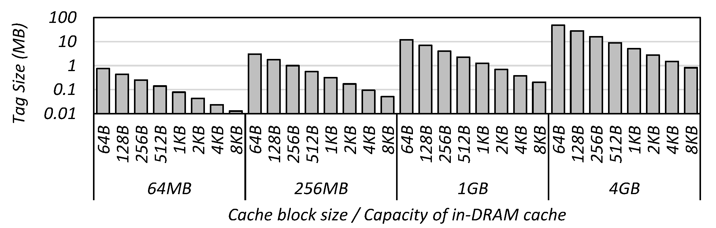
The access time of the tag is influenced by the block size and the capacity of the in-DRAM cache. The larger the cache capacity or the smaller the cache block size, the larger the tag size. Figure 6 shows that the tag size grows from several KB to tens of MB depending on the block size and the capacity.
There are two ways to reduce the tag size. One is to reduce the capacity of the cache, and the other is to increase the cache block size. However, the former is not the ultimate goal of an in-DRAM cache. Therefore, we should increase the cache block size, which has other side-effects. Firstly, a cache block size which is too large can cause significant time overhead and power consumption for the data transfer. Secondly, for applications with low locality, it lowers the hit ratio of the in-DRAM cache. Therefore, it needs to design very sophisticated cache management techniques that considers these aspects.
4. Proposed In-DRAM Cache Management Algorithms
Typical DRAMs use a rank and bank interleaving policy to maximize data bandwidth. It maximizes the reuse rate of any pre-activated row address. This property motivated us to define the block size of the in-DRAM cache as the total data contained in a specific row address of all ranks and banks in the 3D-stacked DRAM. This method is disadvantageous in terms of time and power consumption, because a single data transfer operation moves hundreds of KB of data at the same time. On the other hand, it has the advantage that the tag access time can be reduced by minimizing the tag size. Therefore, it is important to maximize the hit ratio of the in-DRAM cache and to minimize the performance and power damage caused by the transfer. We discuss how to effectively utilize the in-DRAM cache by proposing two new in-DRAM cache management algorithms in the sections below.
4.1. Critical Data Detection and Evaluation Scheme
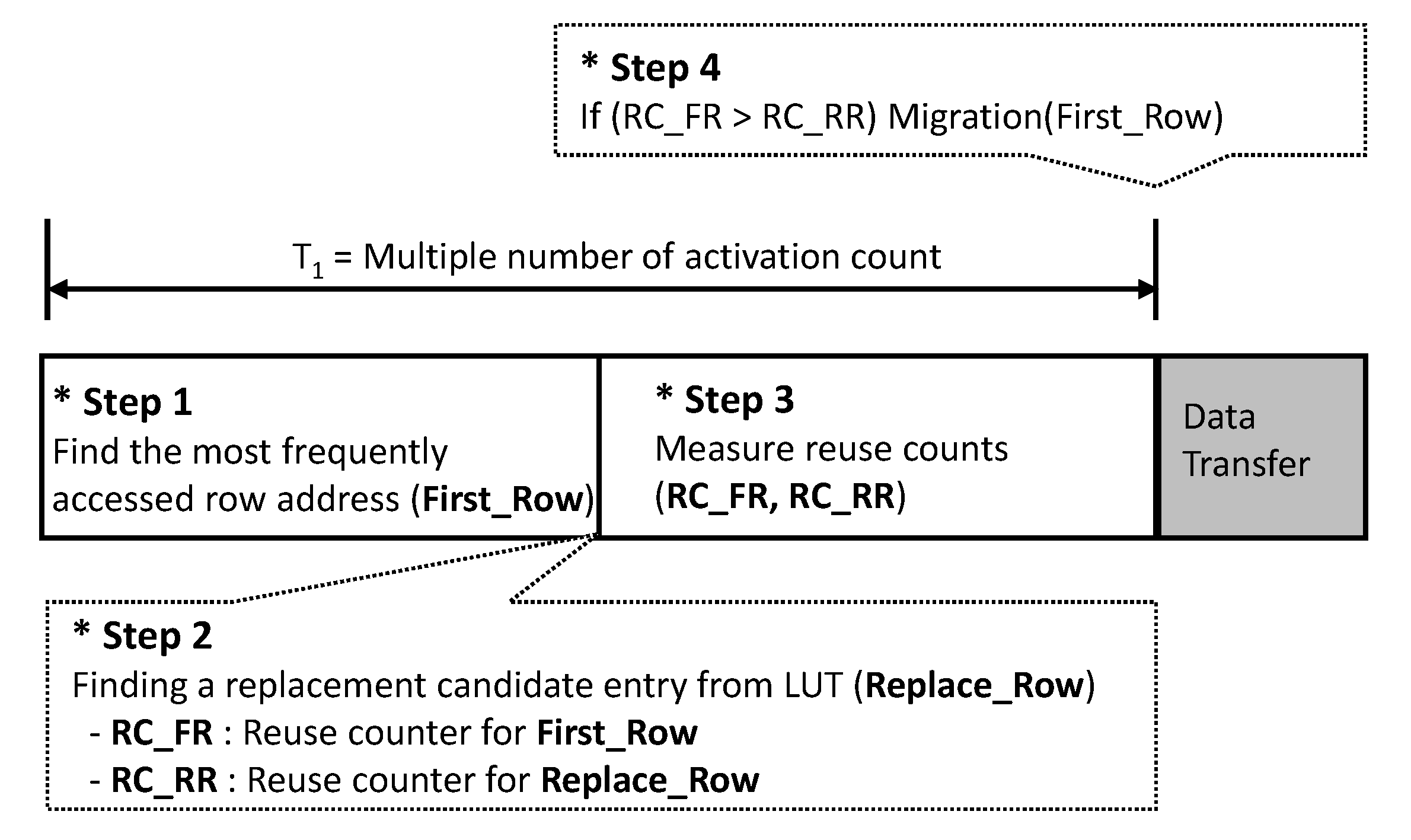
The Critical Data Detection and Evaluation (CDDE) scheme is designed to maximize the hit ratio of an in-DRAM cache. This is a technique that evaluates and replaces the criticality of new data, rather than replacing it with new data unconditionally when a cache miss occurs. Therefore, the proposed technique is divided into the critical data detection stage and evaluation stage. Figure 7 shows the brief description of the proposed algorithm. A unit cycle to determine a data transfer is defined by multiple activation counts, called T. T is divided into four steps, as shown below.
- Step 1: The algorithm finds the most frequently accessed row address (First_Row).
- Step 2: The in-DRAM cache manager selects a candidate entry (Replace_Row) to be replaced in the tag, where the replacement policy can be the least recently used (LRU) or first-in first-out (FIFO) that are similar to the legacy replacement policy [1]. In this paper, we use the FIFO, which can minimize the time delay for the candidate selection.
- Step 3: It measures the reuse counts for the First_Row and Replace_Row, called RC_FR and RC_RR, respectively, to define the more valuable one in terms of reuse.
- Step 4: The manager compares RC_FR and RC_RR and starts the transfer if RC_FR is larger than RC_RR.
The CDDE scheme is an algorithm that allows in-DRAM caches to operate very carefully to maximize hit ratios, but does not consider power consumption due to mass transfer. Therefore, we propose a new in-DRAM cache management scheme that considers power consumption.
4.2. Power-Aware in-DRAM Cache Management Algorithm
Although the operation of the in-DRAM cache increases the power consumption as a result of massive data transfer, it also decreases the operating power owing to the reduced capacitance of the bit-line or shortened signal line between the core and I/O pads. These facts provide us an opportunity to compensate for the increase in transfer power. In other words, if the hit rate of the in-DRAM cache is sufficiently high enough to compensate for the increased transfer power, the overall power of the DRAM device can be maintained constant. In this work, we define several parameters. and represent the amounts of power consumed to access the normal DRAM and in-DRAM cache, respectively. Furthermore, we define the transfer power as and the hit ratio of the in-DRAM cache as HR. Along with the defined parameters, the total DRAM access energy over time of any activation count () is calculated as Equation (1).
Equation (1) indicates that, as the hit rate of the in-DRAM cache increases, the overall access energy decreases. We will fill the reduced energy with transfer energy.
The transfer energy is calculated as shown in Equation (2), where represents the transfer power consumed when the rows of all the ranks and banks are migrated. In addition, the indicates the time needed for a data transfer.
In this paper, we limit the total energy of the proposed scheme to be less than that of normal DRAM devices. Finally, Equation (3) shows the limiting condition.
In Equation (4), all the parameters except HR of the right terms are predefined design parameters. Therefore, if the proposed scheme can monitor HR in real time, the available can be calculated periodically. The in-DRAM cache manager in the DRAM controller controls the T according to Equation (4).
Figure 8 shows the hardware implementation of the proposed scheme. The shaded part—the in-DRAM cache manager—must be added to the normal DRAM controller. The manager controls the timing constraints, such as tRCD, tRP, tAA, tWR, and tRAS when the addresses of the issued commands are included in the tag. The active counter identifies the four stages of CDDE, and the first row detector determines the most frequently accessed row address. Finding the First_Row is done in real time whenever an active row address is entered. The first row detector has as many counters as the number of bits in a row address. For example, if a row address is configured from 0 to 15, there will be a total of 16 counters. Therefore, when a row address is input, only the counters of bits corresponding to 1 out of the 16 bits are incremented by 1. At the end of Step 1 of the CDDE algorithm, the first row detector compares the total number of active inputs and the number of 1’s in each bit during step 1, and sets only the row address bits that are more than half of the active counts to 1. Finally, it returns First_Row consisting only of bits defined as 1 out of 16 bits. The reuse counter has two registers, one for storing the address of First_Row and the other for storing the row address to be replaced. In addition, it has a counter for each register, which increments each counter whenever a row address equal to the value of each register is input. Finally, it defines the more valuable row address in terms of hit rate with the counter output. Our proposed approach is applicable regardless of whether it is an open- or closed-page policy. In other words, the DRAM controllers using an open-page policy do not send multiple active commands continuously for a single row address. However, due to the specification of DRAM which requires only one row address to be activated in one bank, even if the open-page policy is used, there is a high possibility of accessing the same row address discontinuously. The data transfer controller contains a hit history queue (HitQ) and a transfer history queue (TransQ). It finally determines whether or not to execute a transfer according to the power-aware management algorithm.
Our proposed in-DRAM cache structure consists only of tags and data. This is because it can minimize tag access time, which is one of the most important factors of in-DRAM cache. Secondly, because it is not a multilevel structure like a typical cache, the tags do not need bits to store various information. In addition, our proposed in-DRAM cache operates in a write-through manner, minimizing the complexity of the cache itself and eliminating the latency penalty.
The biggest overhead in the in-DRAM cache manager is a tag that occupies from 1.125 KB to 4.5 KB. We used the CATTI tool to calculate its area and leakage power [22]. According to the CACTI tool, for a 32 nm technology, the tag requires 0.05 mm2 and consumes 1.2 mW standby leakage power. In addition, the time overhead of the tag is expected to be 2 ns, which can be minimized because the tag does not have any special information other than the row address and operates in a direct-mapped manner. Since the HitQ and TransQ each consist of 64 entries, we assumed that the area or time overhead could be ignored. The size of the tag may vary depending on the size of the in-DRAM cache. In contrast, the size of the HitQ and TransQ does not depend on the capacity of the in-DRAM cache, which is one of the design parameters.
5. Experimental Results and Discussion
In this paper, we have proposed two new in-DRAM cache management techniques. The ultimate goal of the both is to reduce DRAM latency by achieving maximum in-DRAM cache efficiency within a given energy budget. To evaluate the performance of the proposed techniques, we modeled a computing system including various 3D-stacked DRAM architectures using gem5 and DRAMSim2, a modular platform for computer system architectures [23,24]. Table 1 shows the system and DRAM configurations used in the system simulation of this paper. The cache block size of 256 KB is equal to the total data size contained in a row address of all ranks and banks in the 3D-stacked DRAM. The tag for the in-DRAM cache is implemented in the DRAM controller with a direct-mapped manner by SRAM. We verify the effectiveness of the proposed schemes for various workloads of the PARSEC benchmark suite consisting of multi-threaded programs [25]. Table 2 summarizes the timing constraints for the normal DRAM and in-DRAM cache, where the tAA and tWR of the in-DRAM cache are only applied to the cache-bank architecture.
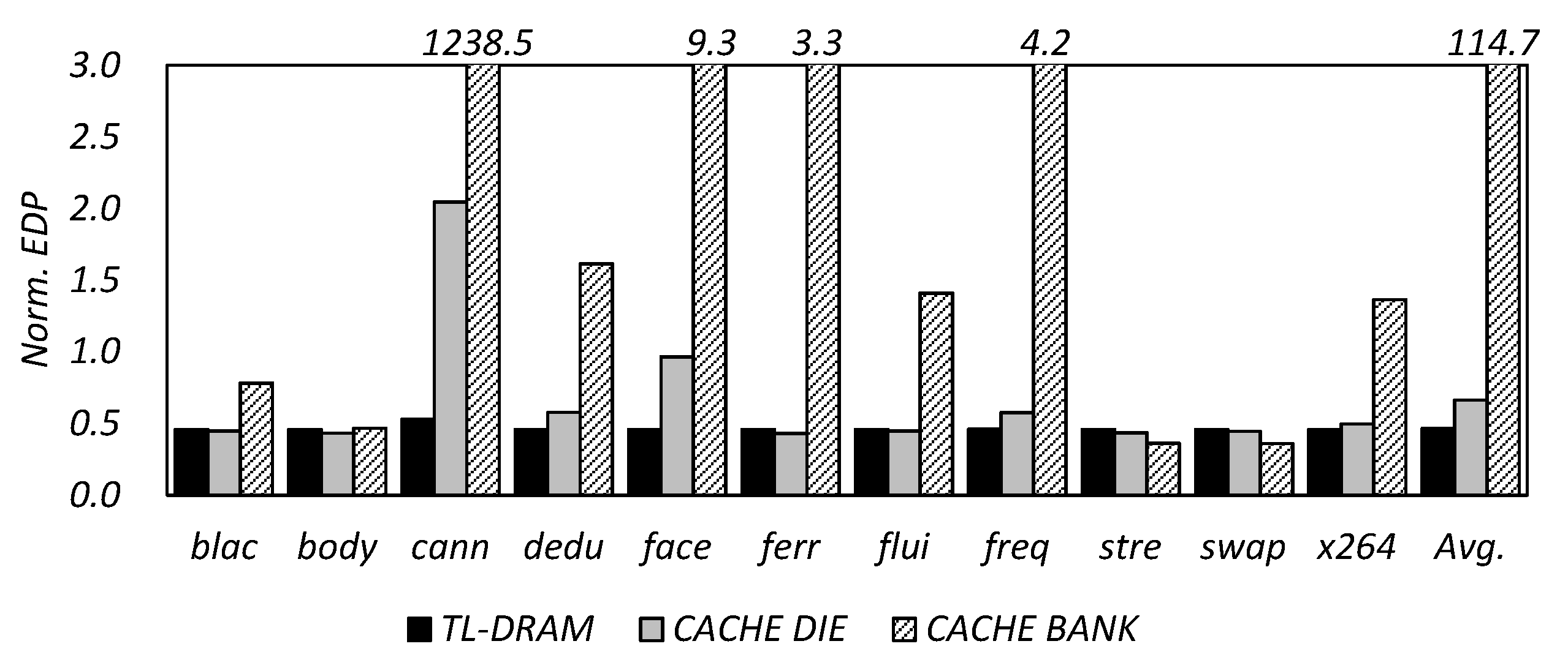
Figure 9 shows the energy delay product (EDP) results for the TL-DRAM, cache die, and cache bank architectures, which are managed by the conventional FIFO cache management (In this paper, all experimental results are normalized for a typical 3D-stacked DRAM without an in-DRAM cache.). As shown in Figure 9, TL-DRAM, which requires low transfer latency and power, has an average of 54% improvement in EDP across all workloads, even when using a conventional cache management scheme. However, for the cache die and cache bank, EDP increases by 2 and 1239 times, respectively, when the most memory-intensive workload canneal is running. That is, if the data locality of the workload is low, data transfer between the cache and the DRAM is more frequent and energy consumption due to the transfer becomes more serious. In particular, such a phenomenon is exacerbated in a cache bank-like structure having a small cache capacity. These results show that typical cache management schemes are not suitable for cache die and cache bank structures, although they may be appropriate for TL-DRAM, and require new algorithms for them.
To evaluate the effectiveness of the CDDE scheme, we experimented with the latency, energy, and EDP performance of 3D-stacked DRAMs with the TL-DRAM, cache die, and cache bank structures for various transfer cycles (T), and Figure 10 shows the results. As shown in Figure 10, TL-DRAM exhibits better latency and EDP performance as the T is smaller, but the cache die and cache bank structure have an optimal T in terms of EDP depending on the properties of the workloads. Since the CDDE scheme helps prevent unnecessary data transfer between the in-DRAM cache and the DRAM, it can achieve better EDP performance over conventional cache management techniques. In addition, CDDE minimizes the EDP performance variation across the workloads compared to conventional management. When applying the conventional management, the difference of normalized EDP is shown to be 0.5 to 1238, according to the data locality (Figure 9). However, when CDDE is applied, it is shown to be 0.5 to 0.9. Despite the benefits of CDDE, it suffers from low EDP efficiency because it has to use a fixed T, even though different Ts have to be applied to each application.
In order to the overcome the drawbacks of CDDE, we implemented the power-aware in-DRAM cache management algorithm and evaluated its performance. Figure 11 shows that the average latency of 3D-stacked DRAMs improved by 22%, 25%, and 28% for the TL-DRAM, cache die, and cache bank, respectively, and EDP by 53%, 53%, and 67%, respectively. Applying the conventional cache management techniques to the in-DRAM cache, TL-DRAM had the best performance with 23% and 54% improvements in latency and EDP, respectively. However, when the proposed CDDE and power-aware management schemes were applied, the EDP of cache bank architecture showed 28% and 67% improvements in latency and EDP, respectively. This implies that although the TL-DRAM has low time and energy consumption for the data transfer, it is not sufficient to improve DRAM latency. In addition, adaptive management techniques, such as CDDE and power-aware which were proposed in this paper, can more effectively reduce DRAM latency in a structure that can basically maximize latency improvement, like cache die and cache bank.
6. Conclusions
Despite the recent introduction of various in-DRAM cache architectures, there was a lack of interest in how to manage them. In this paper, we studied how to derive optimal EDP by maximizing the hit ratio of In-DRAM cache and reducing power consumption due to data transfer. As a result, we achieved an improved EDP of 3D-stacked DRAM up to 67% compared to the conventional cache management scheme. Typical cache management techniques have several limitations when applied to the in-DRAM cache, and the effect depends on the architecture. However, the approach proposed in this paper demonstrates consistent improvements across all architectures.
Author Contributions
H.H.S. designed the architecture and algorithm, and performed the experimental testing. E.-Y.C. supervised the work and provided expertise.
Funding
This work was funded by the National Research Foundation of Korea (NRF), by the Korea government (MSIP) (grant number 2016R1A2B4011799), by the Ministry of Trade, Industry & Energy (MOTIE) (grant number 10080722) and Korea Semiconductor Research Consortium (KSRC) support program for the development of the future semiconductor device and by Samsung Electronics Company, Ltd., Hwasung, Korea.
Conflicts of Interest
The authors declare no conflict of interest.
Abbreviations
The following abbreviations are used in this manuscript:
| DRAM | dynamic random access memory |
| OLTP | on-line transaction processing |
| TSV | through silicon via |
| HBM | high-bandwidth memory |
| HMC | hybrid memory cube |
| SRAM | static random access memory |
| CDDE | critical data detection and evaluation |
| LRU | least recently used |
| FIFO | first-in first-out |
| EDP | energy delay product |
References
- Jacob, B.; Ng, S.; Wang, D. Memory Systems: Cache, DRAM, Disk; Morgan Kaufmann Publishers: Burlington, MA, USA, 2010. [Google Scholar]
- Wulf, W.A.; McKee, S.A. Hitting the Memory Wall: Implications of the Obvious. SIGARCH Comput. Archit. News 1995, 23, 20–24. [Google Scholar] [CrossRef]
- Wilkes, M.V. The Memory Gap and the Future of High Performance Memories. SIGARCH Comput. Archit. News 2001, 29, 2–7. [Google Scholar] [CrossRef]
- JEDEC. DDR SDRAM STANDARD; JEDEC: Arlington, VA, USA, 2008. [Google Scholar]
- JEDEC. DDR2 SDRAM STANDARD; JEDEC: Arlington, VA, USA, 2009. [Google Scholar]
- JEDEC. DDR3 SDRAM STANDARD; JEDEC: Arlington, VA, USA, 2012. [Google Scholar]
- JEDEC. DDR4 SDRAM STANDARD; JEDEC: Arlington, VA, USA, 2017. [Google Scholar]
- Clapp, R.; Dimitrov, M.; Kumar, K.; Viswanathan, V.; Willhalm, T. A Simple Model to Quantify the Impact of Memory Latency and Bandwidth on Performance. In Proceedings of the 2015 ACM SIGMETRICS International Conference on Measurement and Modeling of Computer Systems, Portland, OR, USA, 15–19 June 2015; ACM: New York, NY, USA, 2015; pp. 471–472. [Google Scholar] [CrossRef]
- Zhang, H.; Chen, G.; Ooi, B.C.; Tan, K.L.; Zhang, M. In-Memory Big Data Management and Processing: A Survey. IEEE Trans. Knowl. Data Eng. 2015, 27, 1920–1948. [Google Scholar] [CrossRef]
- Xie, Y.; Loh, G.H.; Black, B.; Bernstein, K. Design space exploration for 3D architectures. ACM J. Emerg. Technol. Comput. Syst. (JETC) 2006, 2, 65–103. [Google Scholar] [CrossRef]
- Kang, U.; Chung, H.J.; Heo, S.; Ahn, S.H.; Lee, H.; Cha, S.H.; Ahn, J.; Kwon, D.; Kim, J.H.; Lee, J.W.; et al. 8Gb 3D DDR3 DRAM using through-silicon-via technology. In Proceedings of the 2009 IEEE International Solid-State Circuits Conference—Digest of Technical Papers, San Francisco, CA, USA, 8–12 February 2009; pp. 130–131. [Google Scholar] [CrossRef]
- Oh, R.; Lee, B.; Shin, S.W.; Bae, W.; Choi, H.; Song, I.; Lee, Y.S.; Choi, J.H.; Kim, C.W.; Jang, S.J.; et al. Design technologies for a 1.2V 2.4Gb/s/pin high capacity DDR4 SDRAM with TSVs. In Proceedings of the 2014 Symposium on VLSI Circuits Digest of Technical Papers, Honolulu, HI, USA, 10–13 June 2014; pp. 1–2. [Google Scholar] [CrossRef]
- JEDEC. HIGH BANDWIDTH MEMORY (HBM) DRAM; JEDEC: Arlington, VA, USA, 2012. [Google Scholar]
- Pawlowski, J.T. Hybrid Memory Cube (HMC). In Proceedings of the 2011 IEEE Hot Chips 23 Symposium (HCS), Stanford, CA, USA, 17–19 August 2011. [Google Scholar]
- Zhang, Z.; Zhu, Z.; Zhang, X. Cached DRAM for ILP processor memory access latency reduction. IEEE Micro 2001, 21, 22–32. [Google Scholar] [CrossRef]
- Kimuta, T.; Takeda, K.; Aimoto, Y.; Nakamura, N.; Iwasaki, T.; Nakazawa, Y.; Toyoshima, H.; Hamada, M.; Togo, M.; Nobusawa, H.; et al. 64 Mb 6.8 ns random ROW access DRAM macro for ASICs. In Proceedings of the 1999 IEEE International Solid-State Circuits Conference, San Francisco, CA, USA, 17 February 1999; pp. 416–417. [Google Scholar] [CrossRef]
- Micron Technology. RLDRAM 2 and 3 Specifications; Micron Technology: Boise, ID, USA, 2004. [Google Scholar]
- Sharroush, S.M.; Abdalla, Y.S.; Dessouki, A.A.; El-Badawy, E.S.A. Dynamic random-access memories without sense amplifiers. e i Elektrotechnik und Informationstechnik 2012, 129, 88–101. [Google Scholar] [CrossRef]
- Lee, D.; Kim, Y.; Seshadri, V.; Liu, J.; Subramanian, L.; Mutlu, O. Tiered-latency DRAM: A low latency and low cost DRAM architecture. In Proceedings of the 2013 IEEE 19th International Symposium on High Performance Computer Architecture (HPCA), Shenzhen, China, 23–27 February 2013; pp. 615–626. [Google Scholar] [CrossRef]
- Son, Y.H.; Seongil, O.; Ro, Y.; Lee, J.W.; Ahn, J.H. Reducing Memory Access Latency with Asymmetric DRAM Bank Organizations. In Proceedings of the 40th Annual International Symposium on Computer Architecture, Tel-Aviv, Israel, 23–27 June 2013; ACM: New York, NY, USA, 2013; pp. 380–391. [Google Scholar] [CrossRef]
- Kim, Y.; Seshadri, V.; Lee, D.; Liu, J.; Mutlu, O. A case for exploiting subarray-level parallelism (SALP) in DRAM. In Proceedings of the 2012 39th Annual International Symposium on Computer Architecture (ISCA), Portland, OR, USA, 9–13 June 2012; pp. 368–379. [Google Scholar] [CrossRef]
- Muralimanohar, N.; Balasubramonian, R.; Jouppi, N.P. CACTI 6.0: A Tool to Model Large Caches. In Proceedings of the 40th Annual IEEE/ACM International Symposium on Microarchitecture, Chicago, IL, USA, 1–5 December 2007. [Google Scholar]
- Binkert, N.; Beckmann, B.; Black, G.; Reinhardt, S.K.; Saidi, A.; Basu, A.; Hestness, J.; Hower, D.R.; Krishna, T.; Sardashti, S.; et al. The Gem5 Simulator. SIGARCH Comput. Archit. News 2011, 39, 1–7. [Google Scholar] [CrossRef]
- Rosenfeld, P.; Cooper-Balis, E.; Jacob, B. DRAMSim2: A Cycle Accurate Memory System Simulator. IEEE Comput. Archit. Lett. 2011, 10, 16–19. [Google Scholar] [CrossRef]
- Bienia, C.; Kumar, S.; Singh, J.P.; Li, K. The PARSEC benchmark suite: Characterization and architectural implications. In Proceedings of the 2008 International Conference on Parallel Architectures and Compilation Techniques (PACT), Toronto, ON, Canada, 25–29 October 2008; pp. 72–81. [Google Scholar]
Figure 1.
Comparison of dynamic random access memory (DRAM) capacity, bandwidth, and latency improvement by DRAM generation [4,5,6,7]. (a) Capacity and bandwidth of DRAM. (b) DRAM access latency: row address to column address delay (tRCD) and row cycle time (tRC).

Figure 2.
Conventional DRAM structure.

Figure 3.
In-DRAM cache architectures.

Figure 4.
Changes in tRCD and tRP according to the various cells per bit line.

Figure 5.
(a) SPICE simulation waveform with 512 cells per bit line, (b) Spice simulation waveform with 64 cells per a bit-line and pre-charge time.
Figure 5.
(a) SPICE simulation waveform with 512 cells per bit line, (b) Spice simulation waveform with 64 cells per a bit-line and pre-charge time.

Figure 6.
Tag-size variation with the block size and the capacity of in-DRAM cache.

Figure 7.
Descriptions of the proposed Critical Data Detection and Evaluation (CDDE) algorithm.

Figure 8.
Implementations of in-DRAM cache manager on the DRAM controller.

Figure 9.
Normalized energy delay product (EDP) results for the TL-DRAM, cache die, and cache bank architecture which are managed by conventional FIFO cache management.
Figure 9.
Normalized energy delay product (EDP) results for the TL-DRAM, cache die, and cache bank architecture which are managed by conventional FIFO cache management.

Figure 10.
Normalized latency, energy, and EDP of TL-DRAM (a), cache die (b), and cache bank (c) structures for various unit cycles (T) with CDDE.
Figure 10.
Normalized latency, energy, and EDP of TL-DRAM (a), cache die (b), and cache bank (c) structures for various unit cycles (T) with CDDE.

Figure 11.
Normalized latency and EDP for the TL-DRAM, cache die, and cache bank architecture with the proposed algorithm. REFs are the latency and EDP results of TL-DRAM with conventional management.
Figure 11.
Normalized latency and EDP for the TL-DRAM, cache die, and cache bank architecture with the proposed algorithm. REFs are the latency and EDP results of TL-DRAM with conventional management.


Table 1.
System and dynamic random access memory (DRAM) configurations.
| CPU Frequency | 2 GHz |
| DRAM Types | DDR3 1600 (800 MHz) |
| DRAM Capacity | 2 GB |
| in-DRAM Cache Capacity | TL-DRAM: 256 MB Cache-die: 512 MB Cache-bank: 128 MB |
| Cache Block Size | 256 KB |
| Tag Size (DRAM controller) | TL-DRAM: 2.25 KB Cache-die: 4.5 KB Cache-bank: 1.125 KB |
| Row Buffer Policy | Adaptive Open Page |
| DRAM cells per a bit line | 512 (DRAM) 64 (in-DRAM cache) |
| DRAM cells per a word line | 1024 |
| Refresh Rate | 64 ms |
| Bit line array structure | Open bit-line |
| Transfer time per a row | 128 * tCCD (5 ns) = 640 ns |
Table 2.
Timing constraints of the normal DRAM and the in-DRAM cache. ACT–activate, PRE–pre-charge, RD–read, WR–write.
Table 2.
Timing constraints of the normal DRAM and the in-DRAM cache. ACT–activate, PRE–pre-charge, RD–read, WR–write.
| Paramter | Symbol | Normal DRAM | in-DRAM Cache |
|---|---|---|---|
| Clock cycle | tCK | 1.25 ns | 1.25 ns |
| ACT to internal RD or WR delay | tRCD | 13.75 ns | 8.75 ns |
| PRE command period | tRP | 13.75 ns | 8.75 ns |
| ACT-to-PRE command period | tRAS | 35.0 ns | 15.0 ns |
| ACT-to-ACT command period | tRC | 48.75 ns | 23.75 ns |
| Internal RD command to data | tAA | 13.75 ns | 8.75 ns |
| Write recovery time | tWR | 15.0 ns | 10.0 ns |
© 2019 by the authors. Licensee MDPI, Basel, Switzerland. This article is an open access article distributed under the terms and conditions of the Creative Commons Attribution (CC BY) license (http://creativecommons.org/licenses/by/4.0/).
Share and Cite
MDPI and ACS Style
Shin, H.H.; Chung, E.-Y. In-DRAM Cache Management for Low Latency and Low Power 3D-Stacked DRAMs. Micromachines 2019, 10, 124. https://doi.org/10.3390/mi10020124
AMA Style
Shin HH, Chung E-Y. In-DRAM Cache Management for Low Latency and Low Power 3D-Stacked DRAMs. Micromachines. 2019; 10(2):124. https://doi.org/10.3390/mi10020124
Chicago/Turabian StyleShin, Ho Hyun, and Eui-Young Chung. 2019. "In-DRAM Cache Management for Low Latency and Low Power 3D-Stacked DRAMs" Micromachines 10, no. 2: 124. https://doi.org/10.3390/mi10020124
Note that from the first issue of 2016, this journal uses article numbers instead of page numbers. See further details here.