High On-Current Ge-Channel Heterojunction Tunnel Field-Effect Transistor Using Direct Band-to-Band Tunneling


1
Department of Electrical and Computer Engineering (ECE), Seoul National University, Gwanak 599, Gwanak-gu, Seoul 151-742, Korea
2
Department of Electrical and Computer Engineering, Ajou University, Suwon 16499, Korea
*
Author to whom correspondence should be addressed.
†
Both authors contributed equally to this manuscript.
Micromachines 2019, 10(2), 77; https://doi.org/10.3390/mi10020077
Submission received: 25 November 2018
/
Revised: 16 January 2019
/
Accepted: 21 January 2019
/
Published: 24 January 2019
(This article belongs to the Special Issue Extremely-Low-Power Devices and Their Applications)
Abstract
:The main challenge for tunnel field-effect transistors (TFETs) is achieving high on-current (Ion) and low subthreshold swing (SS) with reasonable ambipolar characteristics. In order to address these challenges, Ge-channel heterostructure TFET with Si source and drain region is proposed, and its electrical characteristics are compared to other TFET structures. From two-dimensional (2-D) device simulation results, it is confirmed that the Si/Ge heterostructure source junction improves Ion and SS characteristics by using the direct band-to-band tunneling current. Furthermore, the proposed structure shows suppressed ambipolar behavior since the Ge/Si heterostructure is used at the drain junction.
1. Introduction
Metal-oxide-semiconductor field-effect transistors (MOSFETs) have been consistently scaled down to the nanoscale, and power consumption (i.e., power density) is becoming an important concern to maintain Moore’s Law [1]. However, it is increasingly difficult to reduce operating voltage (VDD) while maintaining high on-off current ratio (Ion/Ioff), since there is a fundamental limit of 60 mV/dec subthreshold swing (SS) at room temperature for MOSFETs [2,3]. This is due in part to gate-to-channel coupling limits, which cannot exceed unity due to voltage drop in the gate dielectric, as well as to the carrier injection mechanism, i.e., thermionic emission, which inevitably depends on the Boltzmann statistic [4]. Strategies to achieve SS < 60 mV/dec can be categorized in two ways. For example, negative capacitance field-effect transistor (NCFET) [5,6,7], resistive gate FET (ReFET) [8] and nano-electro mechanical FET (NEMFET) [9,10] mainly focus on the way to improve gate-to-channel coupling (decrease body factor (m) less than 1) with the help of novel gate stacks, while positive feedback FETs [11,12], impact ionization metal-oxide-semiconductor (I-MOS) [13,14] and tunnel FET (TFET) [15,16,17,18] try to change carrier injection mechanism by adopting novel operation methods. Among them, TFETs have received extensive research attention due to their high complementary MOS (CMOS) compatibility and scalability [19,20]. Although TFETs have raised the possibilities that they could succeed MOSFETs, they suffer various technical problems, such as low Ion and disappointing SS. Heterojunction structures, which enable narrower local band-to-band tunneling (BTBT) barrier width (WTUN) by adopting narrow bandgap material like Ge, have been regarded as a powerful solution to address both problems simultaneously [21,22,23,24,25,26]. To the best of our knowledge, all previous heterostructure TFET used Ge at the source region. However, Ion remains significantly behind the requirement for state-of-the-art technology and such device fabrication is not under consideration.
This paper proposes a novel Ge channel heterostructure TFET and shows that the device achieves higher Ion, lower SS, and reasonable ambipolar current (IAMB) using technology computer-aided design (TCAD) simulations. The proposed approach is straightforward: The Si-Ge heterojunction TFET differs from previous proposed systems by adopting Ge at channel not for source. Starting with systematic comparison among other heterojunction and homojunction TFETs’ current-voltage (I-V) characteristics, the proposed TFET’s operation mechanism is rigorously investigated to analyze its superior performance compared to others.
Since the proposed approach is based on the change of channel material, a double gate structure which is highly compatible to the current logic device is used for an analysis (Figure 1). The detailed parameters used in this paper are listed below. In order to exclude short channel effect, physical gate length (LG) and body thickness (TB) between two gates are set at 100 and 20 nm, respectively. For the gate stack, gate oxide with 2 nm equivalent oxide thickness (EOT) and gate contact with 4.05 eV work function (WFN) are used, corresponding to highly doped n-type polysilicon. Source and channel doping concentrations are p-type 1020 cm−3 and undoped, respectively, to improve BTBT efficiency by suppressing degeneracy effect [27] while n-type 1018 cm−3 is used for draining to suppress an ambipolar behavior [28]. The feasibility of proposed TFET for high Ion and steep SS is compared with other TFETs by changing source/channel/drain material combinations, as summarized in Table 1. Considering a simple fabrication process using self-aligned epitaxy, a symmetric device structure is preferred. Therefore, the same materials are selected for the source and drain regions.
In order to analyze the electrical characteristics of the TFETs, two-dimensional (2-D) device simulations are carried out using Synopsys SentaurusTM (Ver. K-2015.06-SP1, Synopsys, Mountain View, CA, USA) [29]. Fermi–Dirac statistics, drift-diffusion carrier transport, Shockley–Read–Hall (SRH) recombination, modified local density approximation (MLDA), and dynamic non-local BTBT models are applied to accurately define device characteristics. Gate leakage current is neglected. The bandgap narrowing model is employed, since the source region is highly doped. Minimum conduction bands of Γ-valley and L-valley of Si and Ge are considered simultaneously. In case of the heterostructure, defects at Si and Ge interfaces are difficult to avoid and can significantly degrade device performance. However, in this research, these defects are neglected since the focus of this manuscript is mainly to optimize the TFET material combination under ideal conditions. For the calculation of BTBT generation rate (G) per unit volume in uniform electric field, Kane’s model is used as follows:
where F is electric field, and F0 = 1 V/cm; P = 2 and 2.5 for the direct and indirect tunneling, respectively. Pre-factor A and exponential factor B parameters for Si and Ge are calibrated by referring [30]. Although Kane’s model has some limitations, such as incorrectness in the presence of nonuniform fields and overestimation of the direct tunneling current [31,32,33], this model remains extensively used for TFET simulations.
2. Result and Discussion
Simulated transfer characteristics for Case1–Case4 with 0.5 V or 0.95 V-drain voltage (VDS) are shown in Figure 2a,b. The drain voltage conditions were selected since they have been widely used in previous TFET studies [24,25,34]. The output characteristics of Case1–Case4 with 0.5 V V-gate voltage (VGS) are shown in Figure 2c. As shown in these figures, Si homojunction TFET (Case1) exhibited poor Ion and SS characteristics, attributed in part to the large tunneling resistance due to the relatively large bandgap (~1.12 eV for Si), and in part to poor BTBT efficiency since Si has an indirect bandgap. In contrast, Ge homojunction TFET (Case2) showed significant Ion and SS improvement, due to the narrower Ge bandgap (~0.67 eV). In addition, Krichnamohan et al. [24] previously showed that Ge can be regarded as having a pseudo-direct bandgap since its conduction band minimum at Γ-valley was only ~0.13 eV higher than that for the L-valley, as shown in Figure 3d. Consequently, BTBT probability is significantly increased and results in up to several hundred μA/μm-Ion. However, Case2 suffered from an increased IAMB since the BTBT resistance at the drain junction was also reduced.
Ge/Si/(Ge) heterojunction (Case3) has been regarded as one of the most promising structures to compromise Ion and Ioff. However, Ion <1 μA/μm requires further improvement to provide reasonable operating speed and IAMB should be significantly reduced. Although Case3 can operate as much as Case2, adopting Ge channel-to-gate overlap region, it requires advanced process capability [28,35].
Proposed TFET (i.e., Case4: Si source and Ge channel) showed better Ion and SS characteristics than Case3 (Ge source and Si channel) structure, as can be seen in Figure 2a,b. It was thoroughly deviated from the general expectations as both WTUN and the tunnel window (i.e., difference between valence band maximum at source and conduction band minimum at channel) of Case4 were larger and smaller than that for Case3, respectively (Figure 3a). On the other hand, Case4 showed similar Ion and SS characteristics to Case2 having Ge homojunction between the source and the channel region. To the best of our knowledge, this is the first report regarding this characteristic for Case4 type structures.
To investigate the reasons of the remarkable transfer characteristics in Case4 structure, tunneling currents in Case3 and Case4 were divided into indirect and direct components, as shown in Figure 3b. For Case3, indirect BTBT dominated total ID and the direct component was negligible when gate voltage (VGS) was higher than 0 V. In contrast, the transfer characteristic of Case4 showed quite a different trend from that of Case3 structure. When VGS = 0 V, the indirect tunneling current was much higher than the direct one. However, as VGS increased, direct BTBT exceeded indirect and total ID, and SS characteristics for Case4 were mainly determined by the direct tunneling current. These results can be further analyzed by the energy band structure at the junction between source and channel. Schematic energy band diagrams of Si and Ge are shown in Figure 3c,d, respectively. When on-current flows in Case3, electrons from the valence band of the Ge source are injected into the conduction band of the Si channel. In contrast, in on-state, electrons in Case4 transfer from the valence band of the Si source to the conduction band of the Ge channel. Therefore, direct BTBT for Case3 barely occurs since the energy level of the Γ valley is 2.28 eV higher than the Δ valley at the conduction band of Si. On the other hand, in case of Si to Ge tunneling junction of Case4 structure, the energy difference between the Γ valley and the L valley at the conduction band of Ge is only 0.14 eV. Hence direct BTBT current can significantly contribute to total ID as VGS increases.
As well as improved Ion and SS characteristics, Case4 (Ge channel and Si drain) structure also exhibited superior ambipolar characteristics compared to Case2 (Ge homojunction) and Case3 structures, as shown in Figure 2. The energy band diagrams for Case2–Case4 structures at off-state (VGS = −0.4 V and VDS = 0.95 V) are shown in Figure 4a, to identify the reason for reduced IAMB in Case4 structure. Interestingly, Case4 structure had minimum WTUN, in contrast to the smallest IAMB in Figure 3b. The main reason for these improved ambipolar characteristics was the effective suppression of direct BTBT components. Direct tunneling leakage of Case4 structure was negligible, confirming Case4 structure’s significantly improved ambipolar characteristics, as seen in Figure 4b.
The electrical characteristics of Case1–Case4 structures are summarized in Table 2. The SS was extracted at 0.95 V-VDS and 0 V-VGS. The Ion and Ioff were defined as ID with 0.95 V-VDS at 1.5 V-VGS and 0 V-VGS, respectively. As discussed above, Case4 exhibited superior Ion/Ioff among the simulated structures, achieving the highest Ion due to direct tunneling at the source junction, and effectively suppressing ambipolar characteristics by reducing direct tunneling leakage current at the drain region. However, the advantages of Case4 structure are limited to n-type TFETs, with p-type TFET exhibiting dominant indirect tunneling with the Ge/Si heterostructure at the source junction.
To fabricate the Si/Ge heterostructure, the Ge layer should be grown by epitaxial processes [23]. Since Ge is confined in the channel region for Case4 structure, this layer can be easily fabricated using self-aligned epitaxial process during the replacement-metal-gate (RMG) process [36]. Ge condensation technique can be applied to implement the high Ge content SiGe channel close to pure Ge [37]. After SiGe layer growth around the channel layer in the RMG process step, the enriched Ge channel layer can be formed by selective Si oxidation and Ge diffusion from the initial grown SiGe layer. In addition, since Si is used for the source region, it is relatively easy to achieve high doping compared to when using Ge.
3. Summary
In this research, the appropriate material combination for source/channel/drain regions in TFET was investigated to improve electrical characteristics. From the device simulation results, it was verified that the Si/Ge/Si combination exhibits outstanding Ion and SS characteristics, using direct BTBT of the Si/Ge heterostructure at the source junction. Additionally, ambipolar effect, one of the critical disadvantages of TFETs, could be suppressed by increasing tunneling resistance at the drain junction with the Ge/Si heterostructure. From the perspective of process complexity, the proposed structure can be easily fabricated using simple self-aligned epitaxy as the same material (Si) is used for the source and drain region.
Author Contributions
Conceptualization, S.K.; Data curation, G.K.; Investigation, G.K. and J.L.; Validation, J.L. and J.H.K.; Visualization, G.K.; Writing-Original Draft Preparation, G.K.; Writing-Review & Editing, J.L., J.H.K. and S.K.
Funding
This research was supported in part by the NRF of Korea funded by the Ministry of Education (MOE), under Grant 2017R1D1A1B03034352 (Basic Science Research Program), in part by the MOTIE/KSRC, under Grant 10080575 (Future Semiconductor Device Technology Development Program) and in part by the MSIT, Korea, under the ITRC support program (IITP-2018-2016-0-00309-002) supervised by the IITP. The EDA tool was supported by the IC Design Education Center (IDEC), Korea.
Conflicts of Interest
The authors declare no conflict of interest.
References
- The International Technology Roadmap for Semiconductors. Available online: http://www.itrs.net/ (accessed on 24 November 2018).
- Lundstrom, M. Device physics at the scaling limit: What matters? In Proceedings of the International Electron Device Meeting (IEDM), Washington, DC, USA, 8–10 December 2003; pp. 789–792. [Google Scholar]
- Frank, D.J.; Robert, R.J.; Nowak, E.; Solomon, P.M.; Taur, Y.; Wong, H.-S.P. Device scaling limits of Si MOSFETs and their application dependencies. Proc. IEEE 2001, 89, 259–288. [Google Scholar] [CrossRef]
- Cheung, K.P. On the 60 mV/dec @300 K Limit for MOSFET Subthreshold Swing. In Proceedings of the Symposium VLSI-TSA Technology Systems and Applications, Hsin Chu, Taiwan, 26–28 April 2010; pp. 72–73. [Google Scholar]
- Li, K.-S.; Chen, P.-G.; Lai, T.-Y.; Lin, C.-H.; Cheng, C.-C.; Chen, C.-C.; Wei, Y.-J.; Hou, Y.-F.; Liao, M.-H.; Lee, M.-H.; et al. Sub-60mV-Swing Negative-Capacitance FinFET without Hysteresis. In Proceedings of the International Electron Device Meeting (IEDM), Washington, DC, USA, 7–9 December 2015; pp. 620–623. [Google Scholar]
- Lin, C.-I.; Khan, A.I.; Salahuddin, S.; Hu, C. Effects of the variation of ferroelectric properties on negative capacitance FET characteristics. IEEE Trans. Electron. Devices 2016, 63, 2197–2199. [Google Scholar] [CrossRef]
- McGuire, F.A.; Cheng, Z.; Price, K.; Franklin, A.D. Sub-60 mV/decade switching in 2D negative capacitance field-effect transistors with integrated ferroelectric polymer. Appl. Phys. Lett. 2016, 109, 093101. [Google Scholar] [CrossRef] [Green Version]
- Huang, Q.; Huang, R.; Pan, Y.; Tan, S.; Wang, Y. Resistive-Gate Field-Effect Transistor: A Novel Steep-Slope Device Based on a Metal—Insulator—Metal—Oxide Gate Stack. IEEE Electron Device Lett. 2014, 35, 877–879. [Google Scholar] [CrossRef]
- Kam, H.; Lee, D.T.; Howe, R.T.; King, T.-J. A new nano-electro-mechanical field effect transistor (NEMFET) design for low-power electronics. In Proceedings of the International Electron Device Meeting (IEDM), Washington, DC, USA, 5–7 December 2005; pp. 463–466. [Google Scholar]
- Abele, N.; Fritschi, N.; Boucart, K.; Casset, F.; Ancey, P.; Ionescu, A.M. Suspended-gate MOSFET: Bringing new MEMS functionality into solid-state MOS transistor. In Proceedings of the International Electron Device Meeting (IEDM), Washington, DC, USA, 5–7 December 2005; pp. 1075–1077. [Google Scholar]
- Padilla, A.; Yeung, C.W.; Shin, C.; Hu, C.; Liu, T.-J.K. Feedback FET: A novel transistor exhibiting steep switching behavior at low bias voltages. In Proceedings of the International Electron Device Meeting (IEDM), San Francisco, CA, USA, 15–17 December 2008; pp. 171–174. [Google Scholar]
- Hwang, S.; Kim, H.; Kwon, D.W.; Lee, J.-H.; Park, B.-G. Si1-xGex positive feedback field-effect transistor with steep subthreshold swing for low-voltage operation. J. Semicond. Technol. Sci. 2017, 17, 216–222. [Google Scholar] [CrossRef]
- Choi, W.Y.; Song, J.Y.; Lee, J.D.; Park, Y.J.; Park, B.-G. 100-nm n-/p-channel I-MOS using a novel self-aligned structure. IEEE Electron Device Lett. 2005, 26, 261–263. [Google Scholar] [CrossRef]
- Ramaswamy, S.; Kumar, M.J. Junction-less impact ionization MOS: Proposal and investigation. IEEE Trans. Electron Devices 2014, 61, 4295–4298. [Google Scholar] [CrossRef]
- Ionescu, A.M.; Riel, H. Tunnel field-effect transistors as energy-efficient electronic switches. Nature 2011, 479, 329–337. [Google Scholar] [CrossRef]
- Choi, W.Y.; Park, B.-G.; Lee, J.D.; Liu, T.-J.K. Tunneling field-effect transistors (TFETs) with subthreshold swing (SS) less than 60 mV/dec. IEEE Electron Device Lett. 2007, 28, 743–745. [Google Scholar] [CrossRef]
- Kim, S.W.; Kim, J.H.; Liu, T.-J.K.; Choi, W.Y.; Park, B.-G. Demonstration of L-shaped tunnel field-effect transistors. IEEE Trans. Electron Devices 2016, 63, 1774–1778. [Google Scholar] [CrossRef]
- Lee, R.; Kwon, D.W.; Kim, S.; Kim, D.H.; Park, B.-G. Investigation of feasibility of tunneling field effect transistor (TFET) as highly sensitive and multi-sensing biosensors. J. Semicond. Technol. Sci. 2017, 17, 141–146. [Google Scholar] [CrossRef]
- Mayer, F.; Le Royer, C.; Damlencourt, J.F.; Romanjek, K.; Andrieu, F.; Tabone, F.C.; Previtali, B.; Deleonibus, S. Impact of SOI, Si1−xGexOI and GeOI substrates on CMOS compatible Tunnel FET performance. In Proceedings of the International Electron Device Meeting (IEDM), San Francisco, CA, USA, 15–17 December 2008; pp. 163–166. [Google Scholar]
- Gandhi, R.; Chen, Z.; Singh, N.; Banerjee, K.; Lee, S. CMOS-compatible vertical-silicon-nanowire gate-all-around ptype tunneling FETs with ≤50-mV/decade subthreshold swing. IEEE Electron Device Lett. 2011, 32, 1504–1506. [Google Scholar] [CrossRef]
- Kim, S.H.; Kam, H.; Hu, C.; Liu, T.-J.K. Germanium-source tunnel field effect transistors with record high ION/IOFF. In Proceedings of the International Conference on VLSI Technology, Kyoto, Japan, 15–18 June 2009; pp. 178–179. [Google Scholar]
- Nayfeh, O.M.; Chleirigh, C.N.; Hennessy, J.; Gomez, L.; Hoyt, J.L.; Antoniadis, D.A. Design of tunneling field-effect transistors using strained-silicon/strained-germanium type-II staggered heterojunctions. IEEE Electron Device Lett. 2008, 29, 1074–1077. [Google Scholar] [CrossRef]
- Han, G.; Guo, P.; Yang, Y.; Zhan, C.; Zhou, Q.; Yeo, Y.-C. Silicon-based tunneling field-effect transistor with elevated germanium source formed on (110) silicon substrate. Appl. Phys. Lett. 2011, 98, 153502. [Google Scholar] [CrossRef]
- Kim, M.; Wakabayashi, Y.; Nakane, R.; Yokoyama, M.; Takenaka, M.; Takagi, S. High Ion/Ioff Ge-source ultrathin body strained-SOI tunnel FETs. In Proceedings of the International Electron Device Meeting (IEDM), San Francisco, CA, USA, 15–17 December 2014; pp. 331–334. [Google Scholar]
- Takagi, S.; Kim, M.; Noguchi, M.; Ji, S.-M.; Nishi, K.; Takenaka, M. III-V and Ge/strained SOI tunnel FET technologies for low power LSIs. In Proceedings of the International Conference on VLSI Technology, Kyoto, Japan, 16–19 June 2015; pp. 22–23. [Google Scholar]
- Krishnamohan, T.; Kim, D.; Raghunathan, S.; Saraswat, K. Double-gate strained-Ge heterostructure tunneling FET (TFET) with record high drive currents and <60 mV/dec subthreshold slope. In Proceedings of the International Electron Device Meeting (IEDM), San Francisco, CA, USA, 15–17 December 2008; pp. 1–3. [Google Scholar]
- Michielis, L.D.; Lattanzio, L.; Ionescu, A.M. Understanding the superlinear onset of tunnel-FET output characteristics. IEEE Electron Device Lett. 2012, 33, 1523–1525. [Google Scholar] [CrossRef]
- Toh, E.-H.; Wang, G.H.; Samudra, G.; Yeo, Y.-C. Device physics and design of double-gate tunneling field-effect transistor by silicon film thickness optimization. Appl. Phys. Lett. 2007, 90, 263507. [Google Scholar] [CrossRef]
- Synopsys, Inc. Sentaurus Device User Guide; Synopsys, Inc.: Mountain View, CA, USA, 2015. [Google Scholar]
- Kao, K.-H.; Verhulst, A.S.; Vandenberghe, W.G.; Sorée, B.; Groeseneken, G.; Meyer, K.D. Direct and indirect band-to-band tunneling in germanium-based TFETs. IEEE Trans. Electron Devices 2011, 59, 292–301. [Google Scholar] [CrossRef]
- Vandenberghe, W.; Soree, B.; Magnus, W.; Fischetti, M.V. Generalized phonon-assisted Zener tunneling in indirect semiconductors with non-uniform electric fields: A rigorous approach. J. Appl. Phys. 2011, 109, 124503. [Google Scholar] [CrossRef] [Green Version]
- Van de Put, M. Band-to-band tunneling in III-V semiconductor heterostructures. In Proceedings of the Eurocon 2013, Zagreb, Croatia, 1–4 July 2013; pp. 2134–2139. [Google Scholar]
- Verreck, D.; Van de Put, M.; Soree, B.; Verhulst, A.S.; Magnus, W.; Vandenberghe, W.; Collaert, N.; Thean, A.; Groeseneken, G. Quantum mechanical solver for confined heterostructure tunnel field-effect transistors. J. Appl. Phys. 2014, 115, 053706. [Google Scholar] [CrossRef]
- Takagi, S.; Kim, M.; Noguchi, M.; Nishi, K.; Takenaka, M. Tunneling FET device technologies using III-V and Ge materials. In Proceedings of the Berkeley Symposiums on Energy Efficient Electronic Systems (E3S), Berkeley, CA, USA, 1–2 October 2015; pp. 1–2. [Google Scholar]
- Kim, S.W.; Choi, W.Y. Hump effects of germanium/silicon heterojunction tunnel field-effect transistors. IEEE Trans. Electron Devices 2016, 63, 2583–2588. [Google Scholar] [CrossRef]
- Pan, J.; Woo, C.; Yang, C.-Y.; Bhandary, U.; Guggila, S.; Krishna, N.; Chung, H.; Hui, A.; Yu, B.; Xiang, Q.; et al. Replacement metal-gate NMOSFETs with ALD TaN/EP-Cu, PVD Ta, and PVD TaN electrode. IEEE Electron Device Lett. 2003, 24, 304–305. [Google Scholar] [CrossRef]
- Vincent, B.; Damlencourt, J.F.; Morand, Y.; Pouydebasque, A.; Le Royer, C.; Clavelier, L.; Dechoux, N.; Rivallin, P.; Nguyen, T.; Cristoloveanu, S.; et al. The Ge condensation technique: A solution for planar SOI/GeOI co-integration for advanced CMOS technologies? Mater. Sci. Semicond. Process. 2008, 11, 205–213. [Google Scholar] [CrossRef]
Figure 1.
Basic schematic of tunnel field-effect transistor (TFET) structure in this study. In order to analyze the performance and the characteristics of the TFETs with two-dimensional device simulation, this kind of double gate structure is used representing the cross-section of the horizontal fin field-effect transistor (FinFET) structure.

Figure 2.
Simulated transfer characteristics ((a) VDS = 0.5 V, (b) VDS = 0.95 V) and output characteristics ((c) VGS = 0.5 V) of Cases1–4.
Figure 2.
Simulated transfer characteristics ((a) VDS = 0.5 V, (b) VDS = 0.95 V) and output characteristics ((c) VGS = 0.5 V) of Cases1–4.

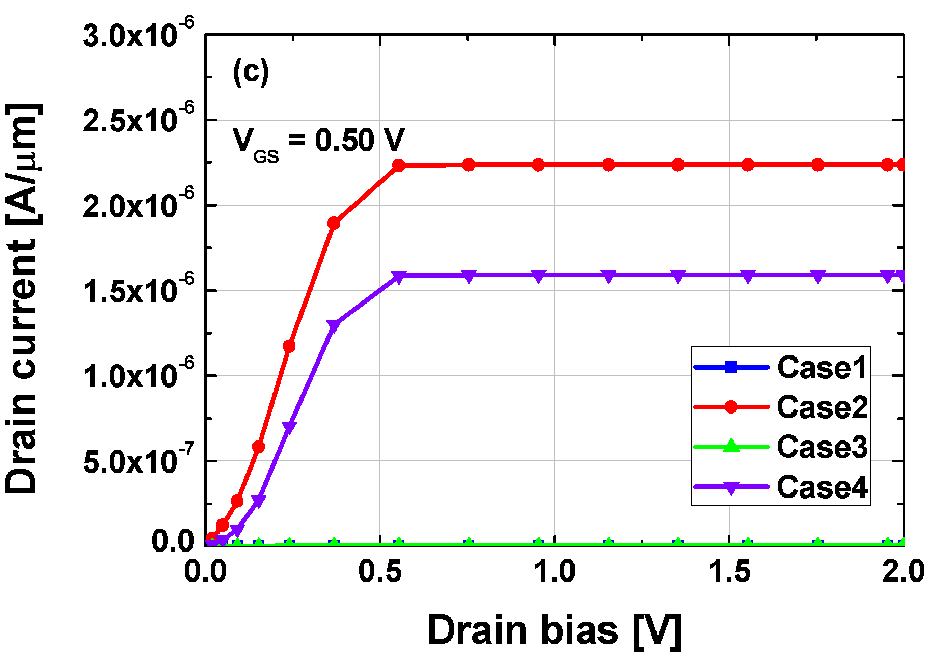
Figure 3.
(a) Energy band diagrams for comparing Case2–Case4 at off-state (VGS = 1.5 V, VDS = 0.95 V). (b) Indirect tunneling, direct tunneling and total ID of Case3 and Case4 structure. (c) Schematic energy band of Si. (d) Schematic energy band of Ge.
Figure 3.
(a) Energy band diagrams for comparing Case2–Case4 at off-state (VGS = 1.5 V, VDS = 0.95 V). (b) Indirect tunneling, direct tunneling and total ID of Case3 and Case4 structure. (c) Schematic energy band of Si. (d) Schematic energy band of Ge.


Figure 4.
(a) Energy band diagrams for comparing Case2–Case4 at off-state (VGS = −0.4 V, VDS = 0.95 V). (b) Indirect tunneling, direct tunneling and total drain current of Case2 and Case4 structures.
Figure 4.
(a) Energy band diagrams for comparing Case2–Case4 at off-state (VGS = −0.4 V, VDS = 0.95 V). (b) Indirect tunneling, direct tunneling and total drain current of Case2 and Case4 structures.


Table 1.
Material combinations of the devices analyzed in this study.
| Case | Source (p-type 1020 cm−3) | Channel (Undoped) | Drain (n-type 1018 cm−3) |
|---|---|---|---|
| Case1 | Si | Si | Si |
| Case2 | Ge | Ge | Ge |
| Case3 | Ge | Si | Ge |
| Case4 | Si | Ge | Si |
Table 2.
Comparison of the electrical characteristics of Case1–Case4 structures.
| Case | Subthreshold Swing (SS) [mV/dec] | Ion [μA/μm] | Ioff [pA/μm] | Ion/Ioff |
|---|---|---|---|---|
| Case1 | 40.5 | 0.1 | 0.001 | 1.0 × 10⁸ |
| Case2 | 45.3 | 294.5 | 0.666 | 4.4 × 10⁸ |
| Case3 | 68.4 | 1.5 | 0.602 | 2.5 × 10⁶ |
| Case4 | 35.8 | 115.1 | 0.095 | 1.2 × 10⁹ |
© 2019 by the authors. Licensee MDPI, Basel, Switzerland. This article is an open access article distributed under the terms and conditions of the Creative Commons Attribution (CC BY) license (http://creativecommons.org/licenses/by/4.0/).
Share and Cite
MDPI and ACS Style
Kim, G.; Lee, J.; Kim, J.H.; Kim, S. High On-Current Ge-Channel Heterojunction Tunnel Field-Effect Transistor Using Direct Band-to-Band Tunneling. Micromachines 2019, 10, 77. https://doi.org/10.3390/mi10020077
AMA Style
Kim G, Lee J, Kim JH, Kim S. High On-Current Ge-Channel Heterojunction Tunnel Field-Effect Transistor Using Direct Band-to-Band Tunneling. Micromachines. 2019; 10(2):77. https://doi.org/10.3390/mi10020077
Chicago/Turabian StyleKim, Garam, Jaehong Lee, Jang Hyun Kim, and Sangwan Kim. 2019. "High On-Current Ge-Channel Heterojunction Tunnel Field-Effect Transistor Using Direct Band-to-Band Tunneling" Micromachines 10, no. 2: 77. https://doi.org/10.3390/mi10020077
Note that from the first issue of 2016, this journal uses article numbers instead of page numbers. See further details here.