Enhancement of Light Extraction Efficiency for InGaN/GaN Light-Emitting Diodes Using Silver Nanoparticle Embedded ZnO Thin Films

1
Institute of Electro-Optical and Material Science, National Formosa University, No. 64, Wunhua Rd., Huwei, Yunlin County 632, Taiwan
2
Department of Microelectronics Engineering, National Kaohsiung University of Science and Technology, Kaohsiung 811, Taiwan
*
Author to whom correspondence should be addressed.
Micromachines 2019, 10(4), 239; https://doi.org/10.3390/mi10040239
Submission received: 19 March 2019
/
Revised: 3 April 2019
/
Accepted: 9 April 2019
/
Published: 10 April 2019
(This article belongs to the Special Issue Nanostructured Light-Emitters)
Abstract
:In this study, we propose a liquid-phase-deposited silver nanoparticle embedded ZnO (LPD-Ag NP/ZnO) thin film at room temperature to improve the light extraction efficiency (LEE) for InGaN/GaN light-emitting diodes (LEDs). The treatment solution for the deposition of the LPD-Ag/NP ZnO thin film comprised a ZnO-powder-saturated HCl and a silver nitrate (AgNO3) aqueous solution. The enhanced LEE of an InGaN/GaN LED with the LPD-Ag NP/ZnO window layer can be attributed to the surface texture and localized surface plasmon (LSP) coupling effect. The surface texture of the LPD-Ag/NP ZnO window layer relies on the AgNO3 concentration, which decides the root-mean-square (RMS) roughness of the thin film. The LSP resonance or extinction wavelength also depends on the concentration of AgNO3, which determines the Ag NP size and content of Ag atoms in the LPD-Ag NP/ZnO thin film. The AgNO3 concentration for the optimal LEE of an InGaN/GaN LED with an LPD-Ag NP/ZnO window layer occurs at 0.05 M, which demonstrates an increased light output intensity that is approximately 1.52 times that of a conventional InGaN/GaN LED under a 20-mA driving current.
1. Introduction
Because gallium-nitride (GaN)-based blue light-emitting diodes (LEDs) have the inherent advantages of a wide bandgap in the green to ultraviolet range, a relatively long lifetime, and low energy consumption, they have received intensive and extensive investigation. InGaN/GaN LEDs with a high light output intensity and low power consumption have been widely applied to products such as solid-state lighting, backlight units for liquid crystal displays, car headlights, traffic lights, and full-color displays [1,2,3,4]. More recently, GaN-based LEDs and solid-state lighting were widely used as transmitting devices in the visible light communication (VLC) system, which has the characteristics of high-speed light communication with low transmission loss, the absence of electromagnetic interference, and license and high security [5,6,7]. A key issue for GaN-based LEDs and solid-state lighting in these applications is a high external quantum efficiency. The external quantum efficiency (EQE), which is the product of the internal quantum efficiency (IQE) and light extraction efficiency (LEE), determines the light output intensity of InGaN/GaN LEDs. The IQE is affected by the concentration of defects, amount of overflow carriers, and spreading area of injection current in the active region. To obtain a modern InGaN/GaN LED with a high IQE, various device structures, such as a designed active region including double-heterostructures and multiple quantum wells (MQWs), the insertion of an electron-blocking layer, and an expanded current-spreading layer, have been investigated [2]. To date, IQEs of higher than 80% have been achieved for InGaN/GaN LEDs because of the rapid development of growth methods and technologies [8,9,10]. The LEE of InGaN/GaN LEDs is also a crucial factor in determining the EQE. The LEE for InGaN/GaN LEDs is very low because of the high index contrast between GaN (n = 2.5) and free space. Several studies have reported that the IQE and LEE of InGaN/GaN LEDs can be enhanced using a patterned sapphire substrate to reflect and adjust the trajectory of light emitting to the sapphire substrate [11,12,13] or flip-chip structured-LEDs to increase the probability of light escaping from the sapphire [14,15]. However, the mechanically and chemically strong nature of sapphire makes patterning a challenging task. In addition, achieving the small dimensions of scattering objects through photolithography technologies is impossible because of the short wavelength of nitride-based LEDs. Some studies [16,17,18,19,20,21] have proposed the fabrication of textured GaN or a window layer to improve the LEE of InGaN/GaN LEDs through the changed trajectory of incident light beyond the escape cone. However, the textured InGaN/GaN LEDs demonstrate deteriorated electrical and temperature properties because of the inhomogeneous spatial field distribution under driving. Moreover, controlling the process and achieving a high repeatability of the rough window layer are difficult tasks. Some studies have reported that photonic crystals [22] and nanopyramids [23] can increase the LEE of InGaN/GaN LEDs through either diffraction or resonant coupling. However, these approaches are not practical because they require technologies that can accurately control the dimension, such as e-beam lithography, which is not suitable for obtaining a high throughput.
Recently, the surface plasmon (SP) coupling effect, which can improve the extraction efficiency of InGaN/GaN LEDs, has received considerable research attention [24,25,26]. SP coupling effects are the collective oscillations of electrons at the interface of a metal and a dielectric, and they can be classified as surface plasmon polaritons (SPPs) at metal surfaces and localized surface plasmons (LSPs) of local oscillation among isolated metallic nanostructures (NPs) with a resonant frequency. The SPP-enhanced LEE of InGaN/GaN LED can be realized by placing a metal layer near InGaN/GaN MQWs [27,28]. However, the inherently high reflection of the metal may block light emission from the InGaN/GaN active region, thus degrading the light output intensity. In contrast, several reports [23,24] have indicated that the LEE of InGaN/GaN blue LEDs can be improved by LSPs. Because the emission wavelength of InGaN/GaN blue LEDs matches the resonance wavelength of LSPs, the photons emitted from the InGaN/GaN active region can be closely coupled with the LSP modes to enhance the light output intensity of InGaN/GaN LED [29,30,31]. The resonant wavelength for the LSPs depends on the metal, such as silver (Ag) for blue, gold (Au) for green, and aluminum (Al) for UV [32,33]. In addition, because the interface is sufficiently rough to scatter the SPs, the coupling energy can be transferred into free space photons.
A well-known method to obtain Ag NPs is the solid-state dewetting process, which transforms an Ag thin film into Ag NPs under a high annealing temperature. However, a high-temperature process may result in the redistribution of the dopant and thermal stress, degrading the performance of devices. We are the first to synthesize a liquid-phase-deposited Ag nanoparticle embedded zinc oxide (LPD-Ag NP/ZnO) thin film through a chemical reaction in an aqueous solution at a low deposition temperature (i.e., even at room temperature) [34]. This method offers several advantages, including a low growth temperature, low cost, large area growth, good step coverage, and simple process and deposition equipment. In this study, the textured surface and LSP coupling effect, which result from the Ag NPs and ZnO in LPD-Ag NP/ZnO thin films, can enhance the LEE of InGaN/GaN LEDs with the LPD-Ag NP/ZnO window layer. The surface texture and LSP coupling effect of an LPD-Ag NP/ZnO thin film depend on the concentration of the silver nitrate (AgNO3) aqueous solution, which determines the root-mean-square (RMS) roughness, Ag content, and Ag NP size of the LPD-Ag NP/ZnO thin film. The measured results indicate that the main factor for enhancing the LEE of InGaN/GaN LEDs with the LPD-Ag NP/ZnO window layer is the LSP coupling effect.
2. Materials and Methods
2.1. Fabrication of InGaN/GaN LEDs with LPD-Ag NPs/ZnO Thin Films
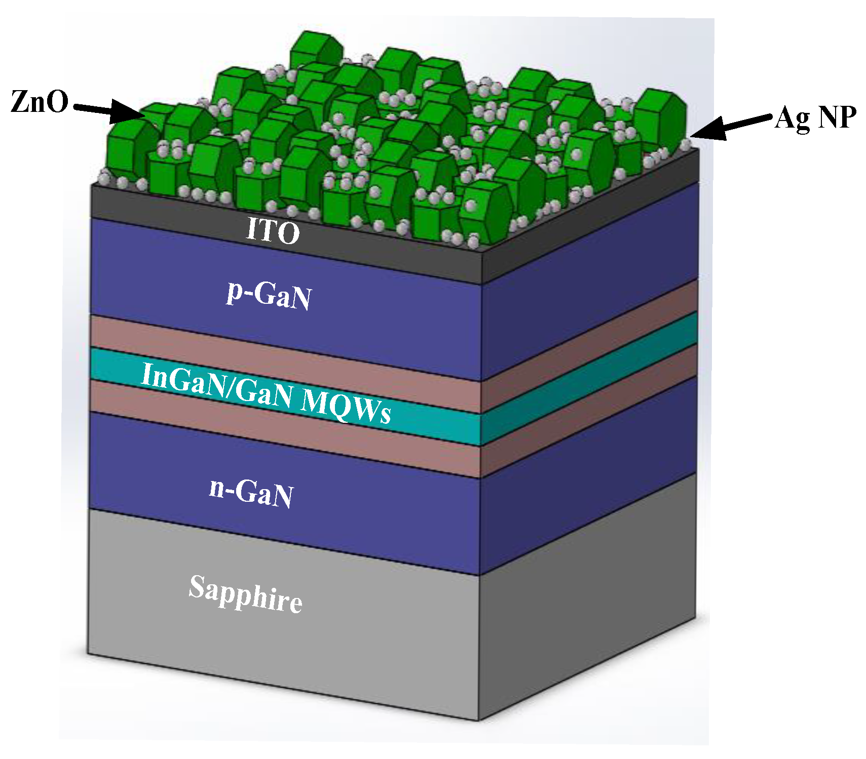
GaN epi-wafers were grown on a c-face (0001) sapphire substrate using a metal-organic chemical vapor deposition (MOCVD) system [29]. The InGaN/GaN LED structure comprises a GaN buffer layer grown at a low temperature, a heavily Si-doped n-type GaN layer, an InGaN/GaN MQW active region, and an Mg-doped p-type GaN layer. Indium-tin-oxide (ITO; Tyntek Co., Hsinchu, Taiwan) was deposited on the p-type GaN layer to form a transparent conductive layer (TCL). The epi-wafers were then patterned using standard photolithographic and partial etching to define the emitting regions. A Ti/Pt/Au alloy was used as ohmic contact metal in the p- and n-GaN contact regions, and the wafer was alloyed in an N2 atmosphere for 5 min at 450 °C. The finished wafer was placed in the treatment solution to deposit the LPD-Ag NPs/ZnO window layer. The size of the emission window for the InGaN/GaN LEDs with ITO TCL and an LPD-Ag NPs/ZnO window layer was 300 × 300 μm2. The schematics of the InGaN/GaN LED with an LPD-Ag NP/ZnO window layer are shown in Figure 1.
2.2. Preparation of Treatment Solution and Growth of LPD-Ag NP/ZnO Thin Films
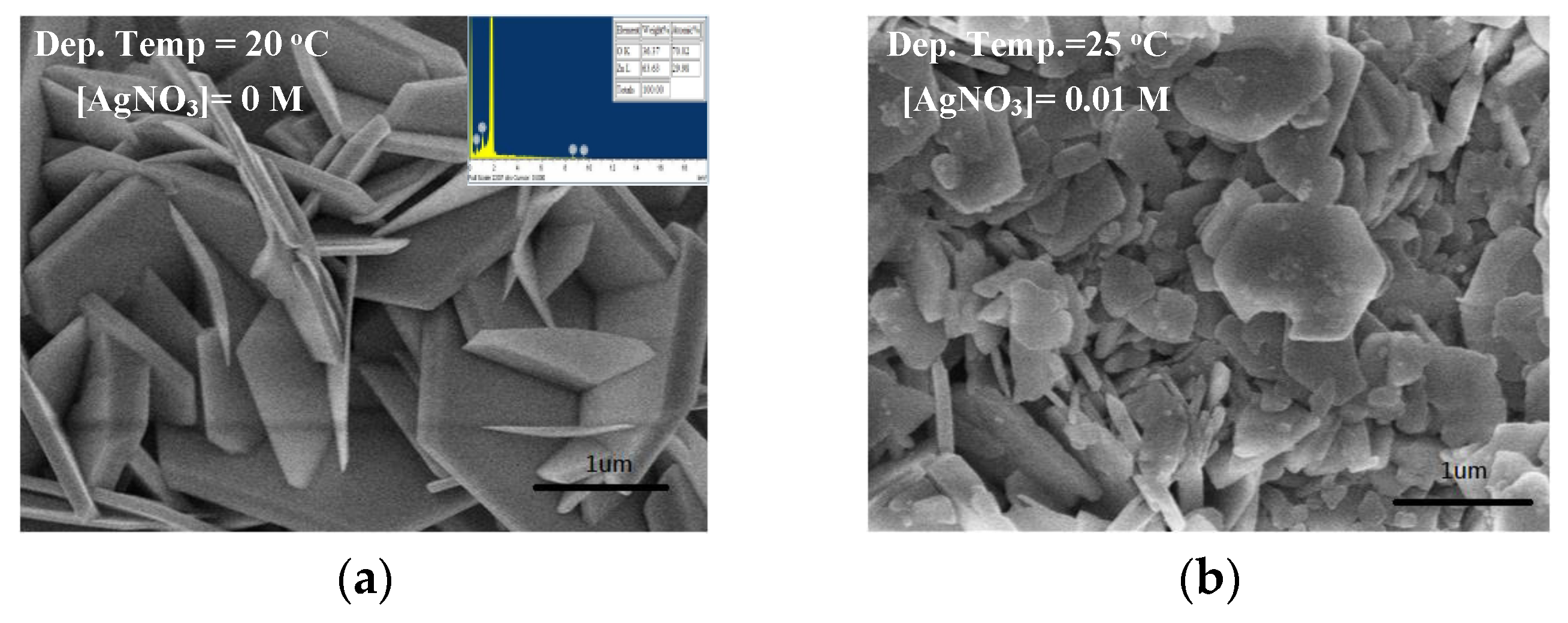
The treatment solution for LPD-Ag NP/ZnO thin films grown on the sapphire substrate was prepared according to the following steps. First, ZnO powder (J. T. Baker) was added into deionized water-diluted HCl (12 M, Taimax, Taiwan), and the mixed solution was then stirred for 1 h at 25 °C to ensure that the HCl solution was saturated with the ZnO powder. Second, a aqueous solution of AgNO3 was added to the ZnO-saturated HCl solution to form the treatment solution. The pH scale of the treatment solution was dominated by the concentration of HCl. The optimum pH scale to grow the LPD-Ag NP/ZnO thin film on the sapphire substrate was approximately 4–5.5. The LPD system for the deposition of the LPD-Ag NP/ZnO thin films comprised a Teflon vessel immersed in a temperature-controlled water bath system. The temperature-controlled water bath system can provide a uniform temperature distribution with an accuracy of 0.1 °C. The following process was implemented to deposit the LPD-Ag NP/ZnO thin film on the InGaN/GaN LED. First, a Teflon vessel containing the treatment solution was placed in the temperature-controlled water bath system at 25 °C for 3–5 min. This preheating step ensured a uniform deposition of the LPD-Ag NP/ZnO thin film on the inserted substrate. Second, the InGaN/GaN LED was inserted in the treatment solution for LPD-Ag NP/ZnO thin film deposition. The surface morphology of LPD-Ag NPs/ZnO on the sapphire substrate was investigated through scanning electron microscopy (SEM), and the Ag content in the LPD-Ag NP/ZnO thin film was detected through energy-dispersive X-ray spectroscopy (EDS).
3. Results and Discussion
To obtain a fair deposition rate, which determines the RMS roughness of the LPD-ZnO thin film, the pH scale of treatment solution and diluted HCl concentration should be maintained at 4–5.5 and 6 M, respectively, during the deposition process and the deposition temperature needs a temperature distribution with an accuracy of 0.1 °C. Figure 2 shows the SEM images for the LPD-ZnO thin film (Figure 2a) and those for the LPD-Ag NP/ZnO thin films deposited at AgNO3 concentrations of 0.01, 0.05, and 0.1 M (Figure 2b–d). The estimated percentages of Ag NP size in the LPD-Ag NP/ZnO thin films deposited at AgNO3 concentrations of 0.05 and 0.1 M are shown in Figure 2e,f. The deposition temperature of the all thin films was 25 °C. The LPD-ZnO thin film exhibited a hexagonal and flake-shaped structure on the sapphire substrate, as shown in Figure 2a. Figure 2b–d show that the structure of the LPD-Ag NP/ZnO thin films reflected the randomly distributed Ag NPs on the hexagonal and flake-shaped ZnO. In addition, Figure 2b–d show that the Ag NP distribution of the LPD-Ag NP/ZnO thin film deposited at a high AgNO3 concentration is denser than that of the thin film deposited at a low AgNO3 concentration. The average size of the randomly distributed Ag NP on the flake-shaped ZnO was approximately 76.8 and 142.6 nm for AgNO3 concentrations of 0.05 and 0.1 M, respectively. The chemical reaction for the LPD-deposited ZnO thin film can be expressed as follows [34,35]:
2ZnO + HCl + 2H2O ⇆ Zn(OH)42− + Zn2+ + H+ + Cl−,
Zn(OH)42 ⇆ ZnO22− + H2O,
The concentration of zinc species including Zn2+ and Zn(OH)42− was used to determine the growth rate of the LPD-ZnO thin film in our previous study [35]. AgNO3 powder can dissolve in H2O and form an Ag-complex, namely Ag(OH)2−, in AgNO3 aqueous solution through the following chemical reactions [36]:
AgNO3 ⇆ Ag+ + NO3−,
Ag+ + 2H2O ⇆ Ag(OH)2− + 2H+,
The Ag-complex reacts with Zn2+ and ZnO22− to form the LPD-Ag NP/ZnO thin film according to the following equation [35,36]:
ZnO22− + Zn2+ + 2Ag(OH)2− ⇆ 2ZnO + 2Ag + 2H2O + 2OH−,
The formation of a flake-shaped ZnO thin film depends on the pH scale of the treatment solution [31]. To obtain a similar flake-shaped ZnO thin film, the pH scale of the treatment solution for LPD-Ag NP/ZnO thin films grown on the sapphire substrate was maintained at 4–5.5. The concentration of Ag+ and Ag(OH)2− in treatment solution depends on the concentration of AgNO3. A high AgNO3 concentration can increase the concentration of Ag(OH)2−, resulting in large and dense Ag NPs embedded on the flake-shaped ZnO.
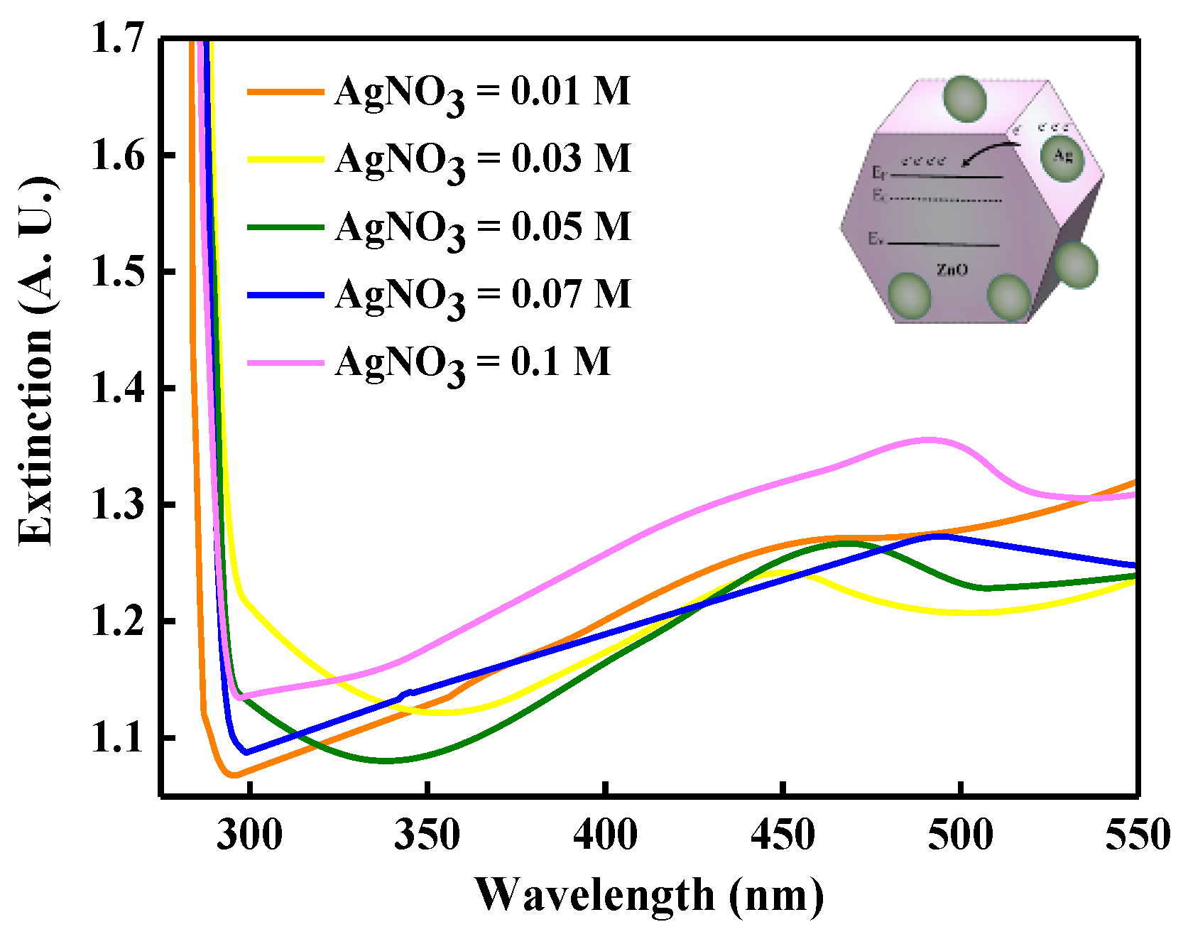
Table 1 lists the Ag contents of LPD-Ag NP/ZnO thin films measured using EDS for various AgNO3 concentrations. The Ag content of LPD-Ag NP/ZnO thin films increased with the AgNO3 concentration, resulting from a high Ag+ concentration, as shown in Equation (3). Moreover, the density of Ag NPs distributed on the flake-shaped ZnO for LPD-Ag NP/ZnO thin films observed from the SEM images exhibited a similar trend to the Ag content of the LPD-Ag NP/ZnO thin films shown in Table 1. We quantitatively determined the density of the Ag NP distributed on the flake-shaped ZnO according to the Ag content of the LPD-Ag NP/ZnO thin films, and we used the varying AgNO3 concentrations of the treatment solution to obtain the specific distribution and size of Ag NPs on the flake-shaped ZnO. However, adding AgNO3 to the treatment solution might cause Ag atoms to dope into the flake-shaped ZnO, rather than form an Ag NP embedded on the flake-shaped ZnO during LPD-Ag NP/ZnO thin film deposition. The extinction-peak position depends on the Ag NP diameter and distance between Ag NPs [32]. Increasing the diameter of Ag NP or decreasing the distance between Ag NPs will shift the extinction-peak wavelength to a long value. Therefore, Ag NPs with a large size or high content under a high AgNO3 concentration result in a red-shift for the extinction-peak, as shown in Table 1. The insets of Figure 2a,c show the EDS spectra for the LPD-ZnO and LPD-Ag NPs/ZnO with an AgNO3 concentration of 0.05 M. The O and Zn atoms contents of the LPD-ZnO thin film were 72.77 and 27.23 at %, respectively, and the compositions of O, Zn, and Ag atoms in the LPD-Ag NPs/ZnO were 70.59, 25.64, and 3.76 at %, respectively. The ratio of O to Zn for the LPD-ZnO thin film (2.67) was similar to that in the LPD-Ag NPs/ZnO thin film (2.75), implying that the Ag NPs were randomly distributed on the flake-shaped ZnO rather than doped during the deposition process.
The photons emitted from the InGaN/GaN active region to the LPD-Ag NP/ZnO window layer were localized along the interface of the randomly-distributed Ag NPs and ZnO. The near-field strength at this interface was enhanced and the incident light from the InGaN/GaN active region was coupled with the LSPs in the Ag NPs. The enhanced light coupled with the LSPs was then decoupled by the Ag NPs and re-emitted into the free space [34]. The wavelength of incident light from the InGaN/GaN active region should be close to the LSP resonant wavelength to enhance the LEE. To determine the LSP resonance wavelength related to the Ag NPs, the measured extinction spectra of the LPD-Ag NP/ZnO thin film are shown in Figure 3 as functions of the AgNO3 concentration. In addition, the diameter of the Ag NPs, the Ag content of the LPD-Ag NP/ZnO thin film, and the peak position of the aforementioned extinction spectra are summarized in Table 1. The peak position of the extinction spectra in Figure 3 reveals an obvious red-shift as the AgNO3 concentration increases from 0.03 to 0.1 M. This is attributed to the following reasons. First, the resonant electromagnetic behavior of the Ag NPs depends on the confinement of conduction electrons to the small particle volume [37]. Because the extinction of light with the wavelength is smaller than that of the diameter of Ag NPs, the electrons move and resonate at a specific frequency (or wavelength), which is called the particle dipole plasmon frequency (or wavelength). As the size of the Ag NPs increases, the conduction electron cannot move in phase, leading to a reduced depolarization field for the red-shift phenomenon. The size of the Ag NPs increases with increasing AgNO3 concentration, resulting in a reduced depolarization field, as indicated in Table 1. Second, the peak position of the absorption or extinction spectrum for Ag NP/ZnO thin films, which depends on the LSP resonant wavelength, can be represented as follows [38,39]:
where λP is the LSP-resonant wavelength, meff is the effective mass of the free electron of the metal, and N is the electron density of metal. The LSP resonant wavelength relates to the electron density of metal. The Ag content increases from 1.64 to 9.46 at % as the AgNO3 concentration increases from 0.03 to 0.1 M, as shown in Table 1. The electron density of the Ag NPs decreases with increasing Ag content (AgNO3 concentration) because electrons move from the Ag NPs to the conduction band of the flake-shaped ZnO, as shown in the inset of Figure 3. According to Equation (6), the reduced electron density of Ag NPs leads to a red-shift phenomenon [40].
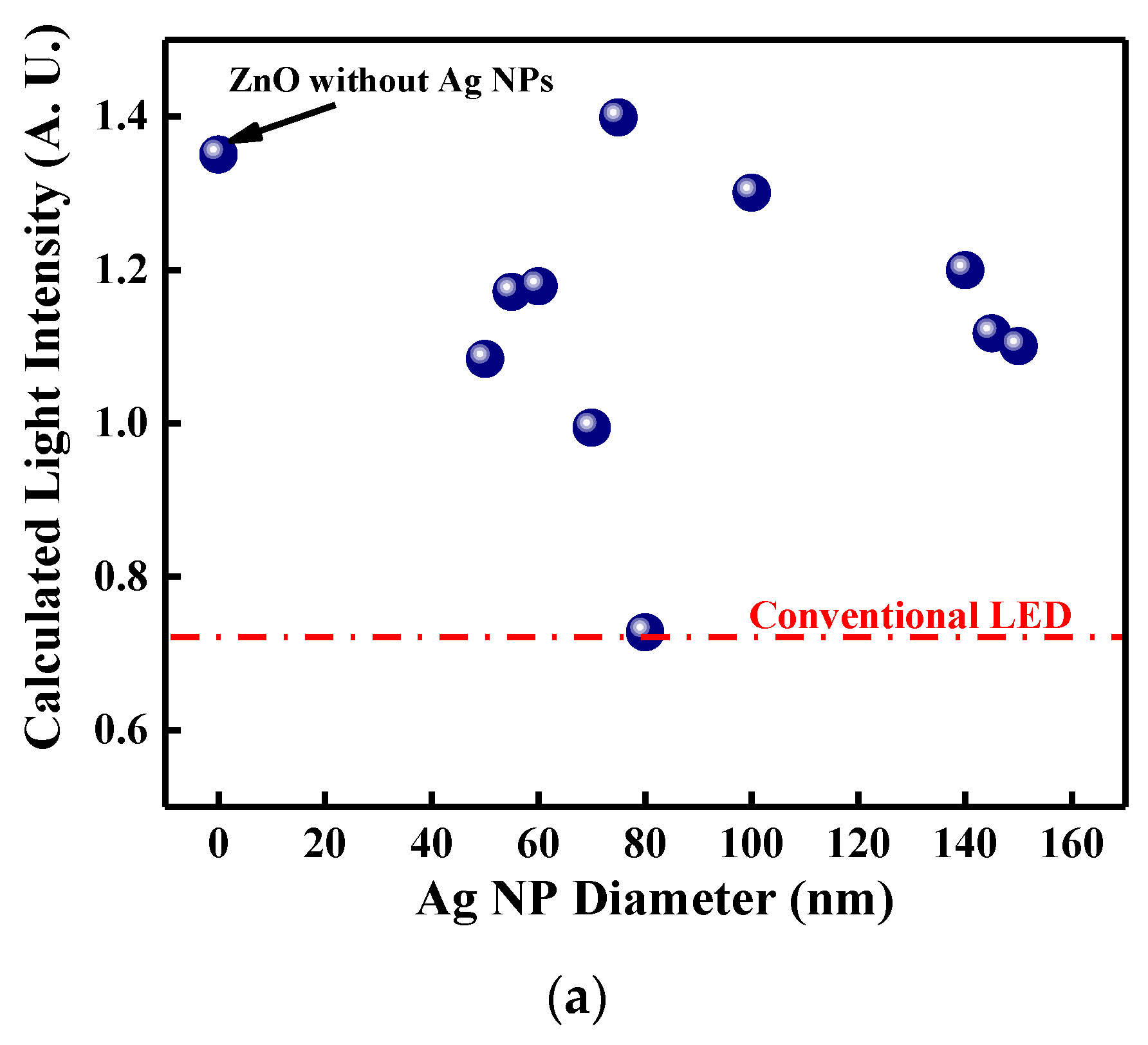
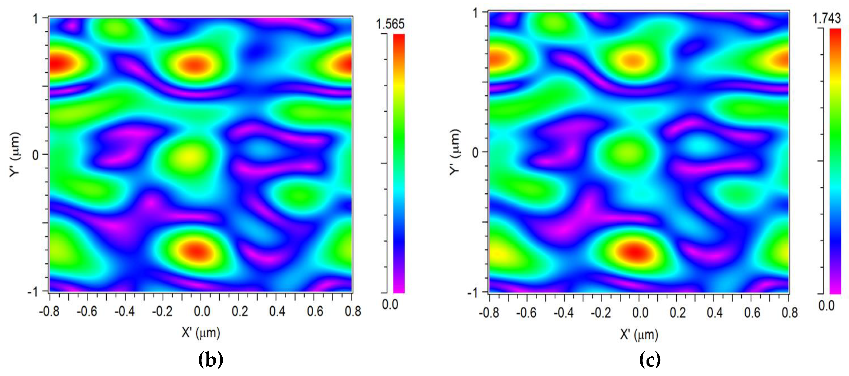
To obtain the optimal AgNO3 concentration, which determines the Ag NP size, to maximize LEE, we used the OptiFDTD computational software, which is based on the finite-difference time-domain, to calculate the optical intensity for InGaN/GaN LEDs with or without the Ag NP/ZnO window layer. A random distribution of Ag NPs with various diameters on the flake-shaped ZnO window layer in InGaN/GaN LED was applied to determine the Ag NP distribution in the LPD-Ag NP/ZnO thin film, as shown in Figure 2. Figure 4a shows the calculated optical intensity of conventional InGaN/GaN LEDs, InGaN/GaN LEDs with the flake-shaped ZnO window layer, and InGaN/GaN LEDs with Ag NPs distributed on the flake-shaped ZnO window layer for Ag NPs with various diameters. The emitting wavelength was set at 460 nm. Figure 4 indicates that the InGaN/GaN LED with Ag NPs distributed on the flake-shaped ZnO thin film achieves the maximum optical intensity when the diameter of the Ag NPs is 75 nm. Figure 4b,c show the electric field distribution of InGaN/GaN LEDs with LPD-ZnO and 75-nm-sized LPD-Ag NP/ZnO window layers. Although the color distribution in Figure 4c is similar to Figure 4b, the scale of the color bar in Figure 4c is larger than that in Figure 4b. These results indicate that an LSP coupling effect is found in InGaN/GaN LED with an LPD-Ag NP/ZnO window layer. Consequently, the enhanced light intensity or LEE might be attributed to the LSP coupling effect of the Ag NPs and the textured LPD-Ag NPs/ZnO thin films, which increase the probability of photons escaping from p-GaN.
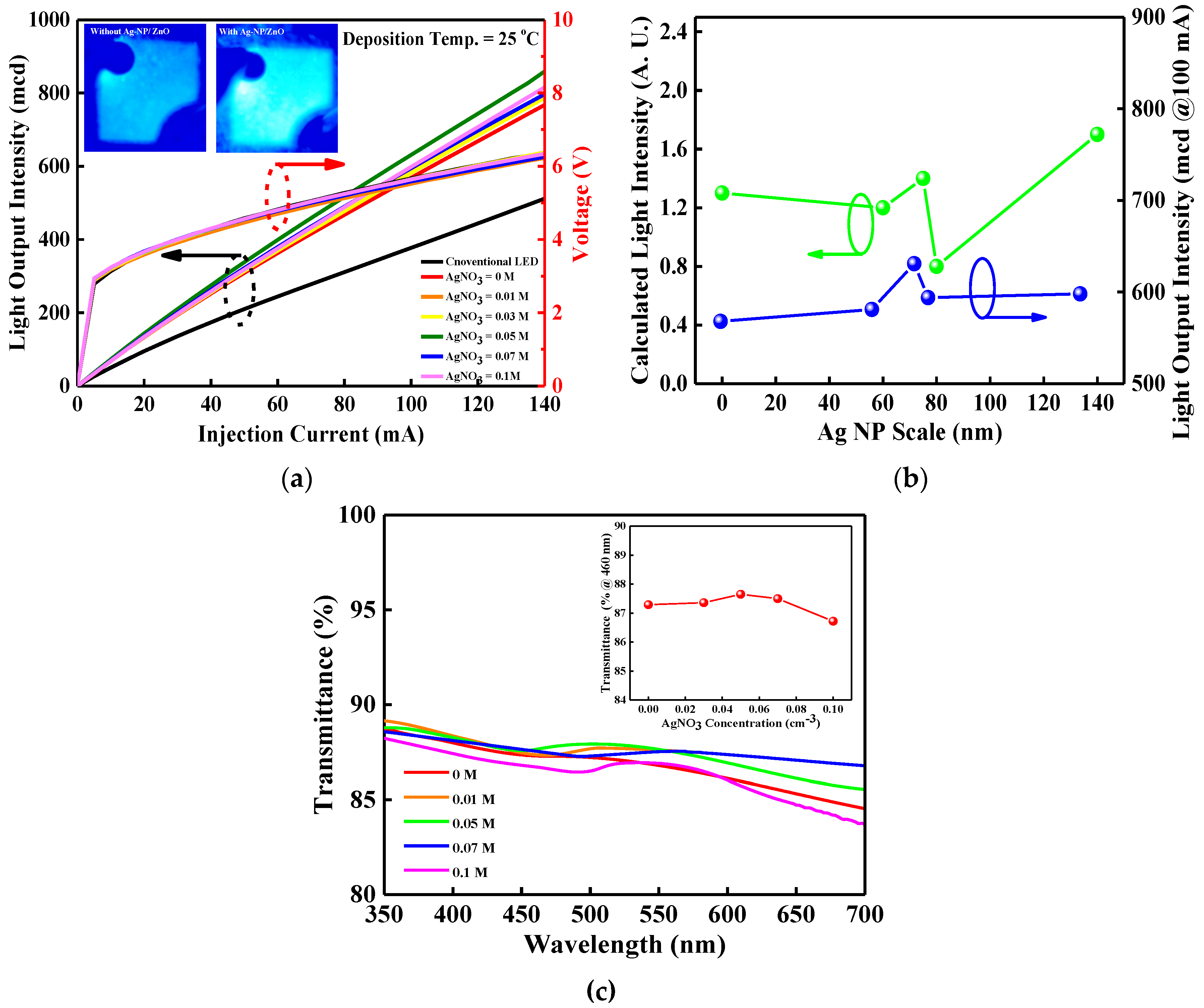
The current–voltage (I–V) and light output intensity–current (L–I) characteristics for the conventional, LPD-ZnO-enhanced, and LPD-Ag NP/ZnO-enhanced InGaN/GaN LEDs are shown in Figure 5a. The forward voltages for the InGaN/GaN LEDs with an LPD-ZnO window layer and LPD-Ag NP/ZnO window layers grown at AgNO3 concentrations of 0.01, 0.03, 0.05, 0.07, and 0.1 M were 3.64, 3.62, 3.65, 3.67, 3.66, and 3.66 V, respectively, at 20 mA, whereas that for the conventional InGaN/GaN LED was 3.58 V at the same driving current level. The forward voltage of the InGaN/GaN LEDs with LPD-ZnO and LPD-Ag NP/ZnO window layers was higher than that for the conventional InGaN/GaN LED because of the deterioration of the ohmic contact resulting from the LPD-ZnO and LPD-Ag NP/ZnO growth on the periphery of the contact. In addition, the series resistance of the InGaN/GaN LEDs with LPD-ZnO and LPD-Ag NP/ZnO window layers was slightly higher than that of conventional InGaN/GaN LED. The series resistance of the InGaN/GaN LEDs depends on the contact metal, metal/ITO interface, ITO, p-GaN, InGaN/GaN active region, and n-GaN, and the increased resistance is caused by the deterioration in the contact during LPD-Ag NP/ZnO deposition. The light output intensities for InGaN/GaN LEDs with an LPD-ZnO window layer and LPD-Ag NP/ZnO window layers grown at AgNO3 concentrations of 0.01, 0.03, 0.05, 0.07, and 0.1 M were 132.9, 133.3, 133.8, 143.5, 136.2, and 134.2 mcd, respectively, for a 20-mA driving current, whereas that for the conventional InGaN/GaN LED was 95.0 mcd at the same driving current. The insets of Figure 5a show the microscope images of light emission for InGaN/GaN LEDs with and without an LPD-Ag NP/ZnO window layer. The light output intensity of the InGaN/GaN LED with an LPD-Ag NP/ZnO window layer was higher than that without an LPD-Ag NP/ZnO window layer because of the improved LEE. Figure 5b represents the calculated light intensity (from Figure 4a) and measured light output intensity (from Figure 5a) under the driving current of 100 mA as a function of Ag NP size. Figure 5c performs the transmittance spectra of LPD-Ag NP/ZnO thin films as a function of AgNO3 concentration over the visible wavelength and the inset of Figure 5c shows the transmittance of LPD-ZnO and LPD-Ag NP/ZnO thin films with the changed AgNO3 concentration at the wavelength of 460 nm. The calculated and measured results indicate that the highest light intensity occurred at the Ag NP size of 75 and 76.8 nm (AgNO3 concentration of 0.05 M) because of the highest transmittance at the 460-nm wavelength shown in the inset of Figure 5c. The highest transmittance can possibly be attributed to the LSP effect [41]. However, the calculated light intensity decreases with Ag NP size increasing form 0 to 60 nm, but the measured light output intensity increases slightly at the same range. This may be attributed to the close transmittance for LPD-ZnO and LPD-Ag NP/ZnO with the Ag NP size of 60 nm, as shown in the inset of Figure 5c. A low Ag NP density on fake-shaped ZnO and a weak LSP effect lead to a slight increase in light output intensity for InGaN/GaN LED with the LPD-Ag NP/ZnO window layer (60-nm AgNP) compared with that with the LPD-ZnO window layer.
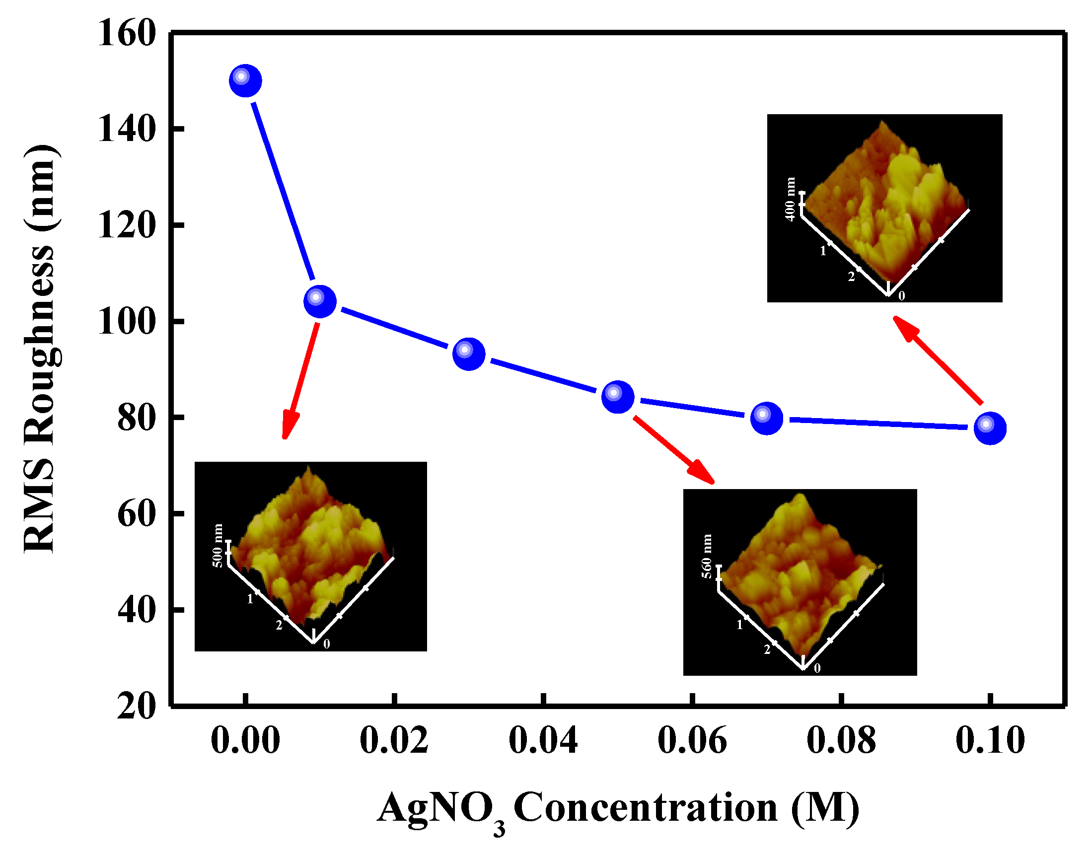
The increased light output intensity may be attributed to the textured surface and LSP coupling effect. It is important to confirm the dominated factor of enhanced LEE for InGaN/GaN LED with an LPD-Ag NP/ZnO window layer. Figure 6 represents the RMS roughness for LPD-Ag NP/ZnO thin films as a function of AgNO3 concentration. The insets of Figure 6 show the AFM images for LPD-Ag NP/ZnO thin films grown at the AgNO3 concentration of 0.01, 0.05, and 0.1 M. In our previous study [31], the LEE of InGaN/GaN LED with an LPD-ZnO window layer depended on the surface texture rather than the ratio of Zn/O. The surface texture depends on the deposition rate of ZnO flake, which was determined by the HCl concentration, and the ratio of Zn/O is almost the same under the varied HCl concentration. Therefore, the enhanced LEE of InGaN/GaN LED caused by the textured LPD-Ag NP/ZnO window layer can be investigated by the RMS roughness. The LEE of an LED gives the ratio of the number of useful emitting-photons to the number of injection charge particles and is defined as [3]
where P is the light output power, I is the injection current, h is the Plank constant, and λ is the emitting wavelength. A textured window layer applied to InGaN/GaN LED can improve the escaped probability of the photons emitted from the InGaN/GaN active region. The RMS roughness of the LPD-Ag NP/ZnO thin film decreases with an increase in the AgNO3 concentration. This is attributed to the following reasons. First, increasing the AgNO3 concentration leads to a large number of Ag NPs aggregated at the interface between ZnO flakes to reduce the RMS roughness of the LPD-Ag NP/ZnO thin film. Secondly, the ZnO flakes in LPD-Ag NP/ZnO thin films tend to bend under a high AgNO3 concentration, resulting in a low RMS roughness. This is attributed to the fact that the concentration of the Ag precursor has a great effect on the morphology of ZnO [42]. LED with a weak textured window layer (with low RMS roughness) shows a lower LEE than that with a strong one (with large RMS roughness) [3]. However, the light output intensity of InGaN/GaN LED increases as the AgNO3 concentration rises from 0 to 0.05 M, as shown in Figure 5. Consequently, the increasing light output intensity of InGaN/GaN LED with an LPD-Ag NP ZnO window layer is attributed to the LSP coupling effect, which occurred because the extinction wavelength was similar to the wavelength of the photon emitted from the InGaN/GaN active region, as shown in Figure 3 [41]. However, further increasing the AgNO3 concentration above 0.07 M reduced the light output intensity because of the weak LSP coupling effect caused by the difference between the resonant wavelength and the emission wavelength from the InGaN/GaN active region. In addition, a strong LSP coupling effect can be obtained by choosing an extinction wavelength similar to and smaller than the emission wavelength from the LED active region.
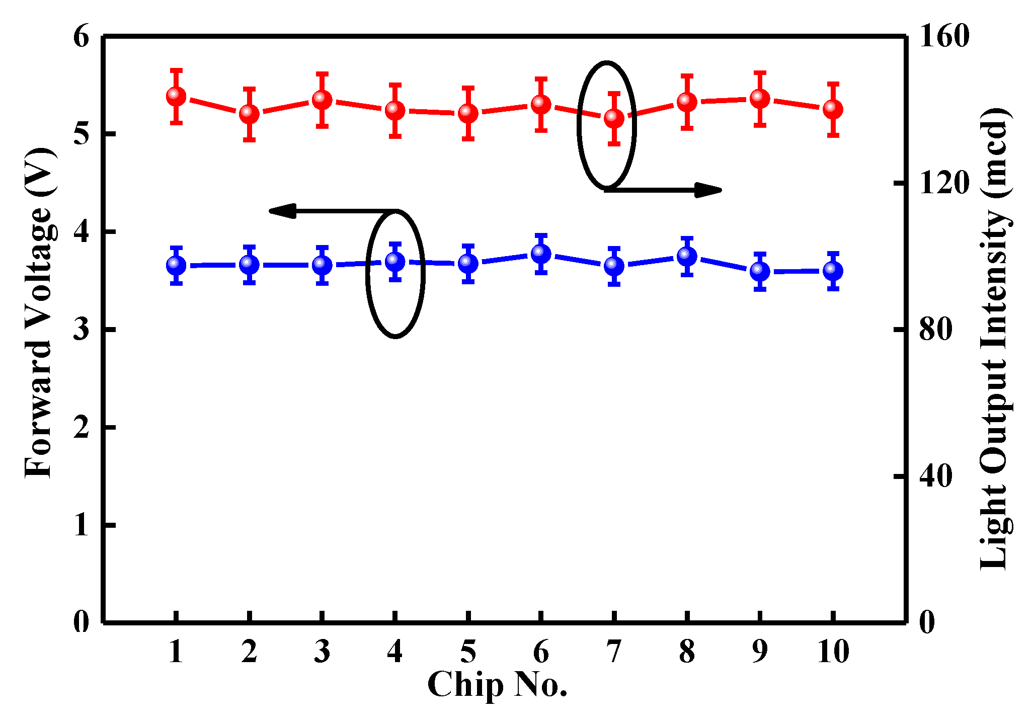
Figure 7 shows the average forward voltage and light output intensity under an injection current of 20 mA for the chosen chips from the InGaN/GaN wafer with the optimal LPD-Ag NP/ZnO and LPD-ZnO window layer for varied runs. The uniformity of the LPD-Ag NP/ZnO thin film on the InGaN/GaN wafer is noteworthy because it is crucial when determining the performance of the InGaN/GaN LEDs. Because the size and distribution of LPD-Ag NPs on the flake-shaped ZnO were similar, the chosen chips from the InGaN/GaN wafer with the optimal LPD-Ag NP/ZnO window layer revealed variations of approximately 5% in the forward voltage and 4.3% in the light output intensity under the same driving current conditions. In addition, the standard deviation of the measured enhancement of emission intensity of the InGaN/GaN wafer with LPD-Ag NP/ZnO to that with LPD-ZnO was about 1.4%.
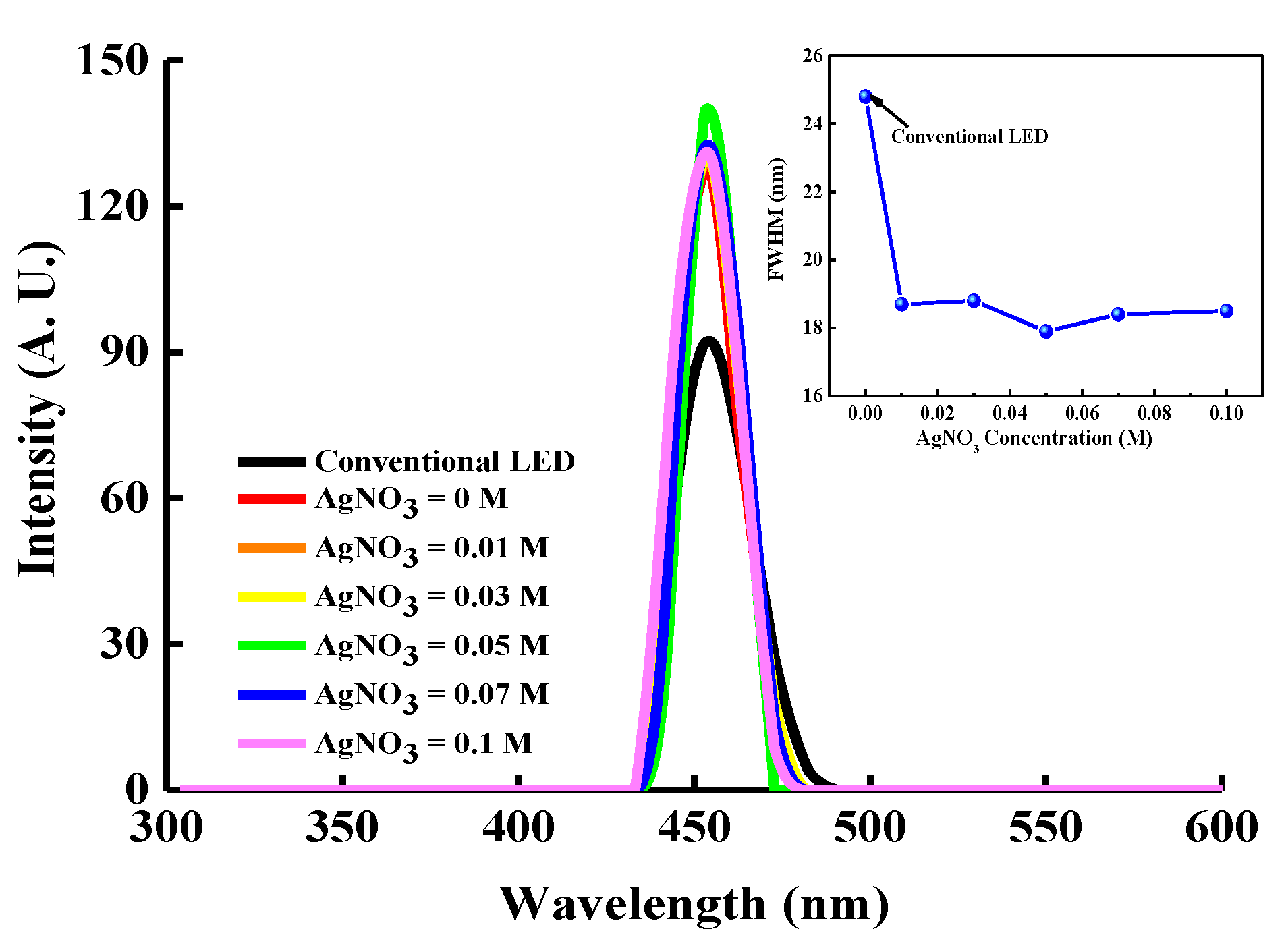
Figure 8 shows the electroluminescence (EL) spectra of the InGaN/GaN LEDs with and without an LPD-Ag NP/ZnO window layer deposited at various AgNO3 concentrations under a 20-mA driving current. The LPD-Ag NP/ZnO thin film deposited at an AgNO3 concentration of 0.05 M exhibited the highest light output intensity because of the LSP coupling effect, and it was approximately 1.52 times higher than that of the conventional InGaN/GaN LEDs. The inset of Figure 8 depicts the full width at half maximum (FWHM) of the EL spectra for the LPD-Ag NP/ZnO-enhanced and conventional InGN/GaN LEDs. The FWHM of the InGaN/GaN LED with an LPD-Ag NP ZnO window layer is narrower than that of a conventional InGaN/GaN LED because of the LSP coupling effect, which can concentrate the emitting spectrum at the resonant wavelength.
4. Conclusions
An LPD-Ag NP/ZnO window layer can enhance the light output intensity of InGaN/GaN LEDs. The improved LEE was attributed to the LSP coupling effect, which was caused by the Ag NPs distributed on the flake-shaped ZnO. The size and distribution of the Ag NPs on the flake-shaped ZnO were adjusted according to the concentration of the AgNO3 aqueous solution that was added to the ZnO-powder-saturated HCl aqueous solution and the pH scale of treatment solution. We quantitatively demonstrated the density of the Ag NPs distributed on the flake-shaped ZnO by determining the Ag content of the LPD-Ag NP/ZnO thin films, because they had similar variations in AgNO3 concentration. The experimental result indicated that the maximum light output intensity occurred when Ag NP with the diameter of approximately 76.8 nm, which is close to the calculated result of Ag NP with the diameter of 75 nm, and with the content of 3.76 at %, were distributed on the flake-shaped ZnO, because the LSP resonance wavelength for this condition was similar to the emission wavelength of the InGaN/GaN LEDs. The light output intensity of the InGaN/GaN LEDs with the optimal LPD-Ag NP/ZnO window layer was 1.52 times higher than that of the conventional InGaN/GaN LED.
Author Contributions
This research was designed and analyzed by L.-P.H. The experimental process and data measurement were performed by Y.-C.D. and Y.-S.J. The data calculation and collection steps were performed by H.-P.C.
Acknowledgments
The authors gratefully acknowledge the financial support of the Ministry of Science and Technology, R. O. C. (107-2221-E-150-033).
Conflicts of Interest
The authors declare no conflict of interest.
References
- Dupuis, R.D.; Krames, M.R. History, Development, and applications of high-brightness visible light-emitting diodes. J. Lightwave Technol. 2008, 26, 1154–1171. [Google Scholar] [CrossRef]
- Li, L.P.; Zhang, Y.H.; Bi, W.G.; Zhang, Z.H.; Kuo, H.C. On the hole injection for III-Nitride based deep ultraviolet light-emitting diodes. Materials 2017, 10, 1221. [Google Scholar] [CrossRef] [PubMed]
- Schubert, E.F. Light–Emitting Diodes, 2nd ed.; Cambridge University Press: Cambridge, UK, 2003. [Google Scholar]
- Koike, M.; Shibata, N.; Kato, H.; Takahashi, Y. Development of high efficiency InGaN/GaN multiquantum-well light-emitting diodes and their application. IEEE J. Sel. Top. Quantum Electron. 2002, 8, 271–277. [Google Scholar] [CrossRef]
- Nikolaevsky, L.; Shchori, T.; Malka, D. Modeling a 1 × 8 MMI Green Light Power Splitter Based on Gallium-Nitride Slot Waveguide Structure. IEEE Photon. Technol. Lett. 2018, 30, 720–723. [Google Scholar] [CrossRef]
- Shoresh, T.; Katanov, N.; Malka, D. 1 × 4 MMI visible light wavelength demultiplexer based on a GaN slot-waveguide structure. Photonic Nanostruct. Fundam. Appl. 2018, 30, 45–49. [Google Scholar] [CrossRef]
- Dadabayev, R.; Shabairou, N.; Zalevsky, Z.; Malka, D. A visible light RGB wavelength demultiplexer based on silicon-nitride multicore PCF. Opt. Laser Technol. 2019, 111, 411–416. [Google Scholar] [CrossRef]
- Ngo, T.H.; Chery, N.; Valvin, P.; Courville, A.; Mierry, P.; Damilano, B.; Ruterana, P.; Gil, B. Internal quantum efficiency in polar and semipolar (11–22) InxGa1-xN/InyGa1-yN quantum wells emitting from blue to red. Superlattices Microstruct. 2018, 113, 129–134. [Google Scholar] [CrossRef]
- Ryu, H.Y.; Ryu, G.H.; Choi, Y.H.; Ma, B.J. Modeling and simulation of efficiency droop in GaN-based blue lightemitting diodes incorporating the effect of reduced active volume of InGaN quantum wells. Curr. Appl. Phys. 2017, 17, 1298–1302. [Google Scholar] [CrossRef]
- Koronski, K.; Strak, P.; Wierzbicka, A.; Grzanka, E.; Borysiuk, J.; Sobczak, K.; Jakiela, R.; Sobanska, M.; Klosek, K.; Monroy, E.; et al. Experimental and theoretical analysis of influence of barrier composition on optical properties of GaN/AlGaN multi-quantum wells: Temperature- and pressure-dependent photoluminescence studies. J. Alloys Compd. 2018, 769, 1064–1071. [Google Scholar] [CrossRef]
- Zhou, Q.B.; Xu, M.S.; Li, Q.X.; Wang, H. Improved efficiency of GaN-based green led by a nano-micro complex patterned sapphire substrate. IEEE Photonic Technol. Lett. 2017, 29, 983–986. [Google Scholar] [CrossRef]
- Liou, J.K.; Chen, W.C.; Chang, C.H.; Chang, Y.C.; Tsai, J.H.; Liu, W.C. Enhanced light extraction of a high-power GaN-based light-emitting diode with a nanohemispherical hybrid backside reflector. IEEE Trans. Electron Dev. 2015, 62, 3296–3301. [Google Scholar] [CrossRef]
- Huang, S.W.; Chang, C.C.; Lin, H.Y.; Li, X.F.; Lin, Y.C.; Liu, C.Y. Fabrication of nano-cavity patterned sapphire substrate using self-assembly meshed Pt thin film on c-plane sapphire substrate. Thin Solid Film 2017, 628, 127–131. [Google Scholar] [CrossRef]
- Zhou, S.J.; Zheng, C.J.; Lv, J.J.; Gao, Y.L.; Wang, R.Q.; Liu, S. GaN-based flip-chip LEDs with highly reflective ITO/DBR p-type and via hole-based n-type contacts for enhanced current spreading and light extraction. Opt. Laser Technol. 2017, 92, 95–100. [Google Scholar] [CrossRef]
- Chang, S.J.; Lin, N.M.; Shei, S.C. GaN-based power flip-chip LEDs with SILAR and hydrothermal ZnO nanorods. IEEE J. Sel. Top. Quantum Electron. 2015, 21, 9100405. [Google Scholar]
- Lin, T.S.; Wang, S.J.; Hung, C.H. Enhanced light extraction of GaN-based vertical LEDs with patterned trenches and nanostructures. Mater. Sci. Semicond. Process. 2017, 57, 77–82. [Google Scholar] [CrossRef]
- Uthirakumar, P.; Kang, J.H.; Ryu, B.D.; Kim, H.G.; Hong, C.H. Nanoscale ITO/ZnO layer-texturing for high-efficiency InGaN/GaN light emitting diodes. Mater. Sci. Eng. B 2010, 166, 230–234. [Google Scholar] [CrossRef]
- Lee, T.X.; Chou, C.C. Scale-dependent light scattering analysis of textured structures on LED light extraction enhancement using hybrid full-wave finite-difference time-domain and ray-tracing methods. Energy 2017, 10, 424. [Google Scholar] [CrossRef]
- Xu, K.; Xie, Y.Y.; Ma, H.L.; Du, Y.X.; Zeng, F.G.; Ding, P.; Gao, Z.Y.; Xu, C.; Sun, J. ZnO nanorods/graphene/Ni/Au hybrid structures as transparent conductive layer in GaN LED for low work voltage and high light extraction. Solid-State Electron. 2016, 126, 5–9. [Google Scholar] [CrossRef]
- Yang, Y.B.; Ren, Y.; Chen, Y.X.; Liu, M.G.; Chen, W.J.; Han, X.B.; Lin, X.Q.; Liao, Q.; Zang, W.J.; Lou, H.; et al. Light output enhancement of GaN-based light-emitting diodes by maskless surface roughening. Microelectron. Eng. 2015, 139, 39–42. [Google Scholar] [CrossRef]
- Byeon, K.J.; Cho, J.Y.; Jo, H.B.; Lee, H. Fabrication of high-brightness GaN-based light-emitting diodes viathermal nanoimprinting of ZnO-nanoparticle-dispersed resin. Appl. Surf. Sci. 2015, 346, 354–360. [Google Scholar] [CrossRef]
- Lei, P.H.; Yang, C.D.; Yang, Y.S.; Lin, J.H. Preparation of a periodic polystyrene nanosphere array using the dip-drop method with post-deposition etching and its application of improving light extraction efficiency of InGaN/GaN LEDs. Nanoscal. Res. Letts. 2018, 13, 180. [Google Scholar] [CrossRef] [PubMed]
- Mikulics, M.; Winden, A.; Marso, M.; Moonshiram, A.; Luth, H.; Grutzmacher, D.; Hardtdegen, H. Nano-light-emitting-diodes based on InGaN mesoscopic structures for energy saving optoelectronics. Appl. Phys. Letts. 2016, 109, 041103. [Google Scholar] [CrossRef]
- Fadil, A.; Iida, D.; Chen, Y.T.; Ou, Y.Y.; Kamiyama, S.; Ou, H.Y. Influence of near-field coupling from Ag surface plasmons on InGaN/GaN quantum-well photoluminescence. J. Lumin. 2016, 175, 213–216. [Google Scholar] [CrossRef]
- Li, Y.F.; Wang, S.A.; Su, X.L.; Tang, W.H.; Li, Q.A.; Guo, M.F.; Zhang, Y.; Zhang, M.Y.; Yun, F.; Hou, X. Efficiency droop suppression of distance-engineered surface plasmon-coupled photoluminescence in GaN-based quantum well LEDs. AIP Adv. 2017, 7, 115118. [Google Scholar] [CrossRef]
- Lu, C.H.; Wu, S.E.; Lai, Y.L.; Li, Y.L.; Liu, C.P. Improved light emission of GaN-based light-emitting diodes by efficient localized surface plasmon coupling with silver nanoparticles. J. Alloys Compd. 2014, 585, 460–464. [Google Scholar] [CrossRef]
- Zhao, H.P.; Zhang, J.; Liu, G.Y.; Tansu, N. Surface plasmon dispersion engineering via double-metallic Au/Ag layers for III-V nitride based light-emitting diodes. Appl. Phys. Lett. 2011, 98, 151115. [Google Scholar] [CrossRef]
- Zhang, H.S.; Zhu, J.; Zhu, Z.D.; Li, Q.Q.; Jin, G.F. Surface-plasmon-enhanced GaN-LED based on the quasi-symmetrical planar waveguide structure. Opt. Commun. 2013, 311, 311–316. [Google Scholar] [CrossRef]
- Hsieh, C.; Yao, Y.F.; Chen, C.F.; Shih, P.Y.; Lin, C.H.; Su, C.Y.; Chen, H.S.; Chen, C.H.; Yu, C.K.; Kiang, Y.W.; et al. Localized surface plasmon coupled light-emitting diodes with buried and surface Ag nanoparticles. IEEE Photonics Technol. Lett. 2014, 26, 1699–1702. [Google Scholar] [CrossRef]
- Niu, B.J.; Wu, L.L.; Tang, W.; Zhang, X.T.; Meng, Q.G. Enhancement of near-band edge emission of Au/ZnO composite nanobelts by surface plasmon resonance. Cryst. Eng. Commun. 2011, 13, 3678–3681. [Google Scholar] [CrossRef]
- Cho, C.Y.; Hong, S.H.; Park, S.J. Improvement of optical and electrical properties of indiumtin oxide layer of GaN-based light-emitting diode by surface plasmon in silver nanoparticles. Thin Solid Films 2015, 590, 76–79. [Google Scholar] [CrossRef]
- Lee, I.H.; Jang, L.W.; Polyakov, A.Y. Performance enhancement of GaN-based light emitting diodes by the interaction with localized surface plasmons. Nano Energy 2015, 13, 140–173. [Google Scholar] [CrossRef]
- Tateishi, K.; Funato, M.; Kawaka, Y.; Okamoto, K.; Tamada, K. Highly enhanced green emission from InGaN quantum wells due to surface plasmon resonance on aluminum films. Appl. Phys. Lett. 2015, 106, 121112. [Google Scholar] [CrossRef]
- Lei, P.H.; Lee, Y.C.; Lin, C.T. Enhanced extraction efficiency of InGaN/GaN light-emitting diodes by liquid phase-deposited zinc-oxide-textured window layer. IEEE Trans. Electron. Dev. 2012, 59, 1672–1678. [Google Scholar]
- Yao, T.; Hong, S.K. Advance in Material Research 12 Oxide and Nitride Semiconductors Processing, Properties, and Applications; Springer: New York, NY, USA, 2009. [Google Scholar]
- Xie, J.S.; Wu, Q.S. One-pot synthesis of ZnO/Ag nanospheres with enhanced photocatalytic activity. Mater. Lett. 2010, 64, 389–392. [Google Scholar] [CrossRef]
- Zhang, S.G.; Zhang, X.W.; Yin, Z.G.; Si, F.T.; Gao, H.L.; Dong, J.J.; Liu, X. Optimization of electroluminscence from n-ZnO/AlN/p-GaN light-emitting diodes by tailoring Ag localized surface plasmon. J. Appl. Phys. 2012, 112, 013112. [Google Scholar] [CrossRef]
- Shan, G.; Xu, L.H.; Wang, G.R.; Liu, Y. Enhanced Raman scattering of ZnO quantum dots on silver colloids. J. Phys. Chem. 2007, C111, 3290–3293. [Google Scholar] [CrossRef]
- Xie, W.; Li, Y.Z.; Sun, W.; Huang, J.C.; Xie, H.; Zhao, X.J. Surface modification of ZnO with Ag improves its photocatalytic efficiency and photostability. J. Photochem. Photobiol. A 2010, 216, 149–155. [Google Scholar] [CrossRef]
- Han, Z.Z.; Ren, L.L.; Cui, Z.H.; Chen, C.Q.; Pan, H.B.; Chen, J.Z. Ag/ZnO flower heterostructures as a visile-light driven photocatalyst via surface plasmon resonance. Appl. Catal. B 2012, 126, 298–305. [Google Scholar] [CrossRef]
- Yu, Z.Z.; Li, Q.; Fan, Q.G.; Zhu, Y.X. Investigation on surface-plasmon-enhanced light emission of InGaN/GaN multiple quantum wells. Superlattices Microstruct. 2018, 117, 200–206. [Google Scholar] [CrossRef]
- Shan, G.Y.; Zheng, S.J.; Chen, S.P.; Chen, Y.W.; Liu, Y.C. Multifunctional ZnO/Ag nanorod array as highly sensitive substrate for surface enhanced Raman detection. Colloid Surf. B Biointerface 2012, 94, 157–162. [Google Scholar] [CrossRef]
Figure 1.
The schematics of InGaN/GaN LED with an LPD-Ag NP/ZnO window layer.

Figure 2.
SEM images for (a) LPD-ZnO and LPD-Ag NP/ZnO thin films under AgNO3 concentrations of (b) 0.01, (c) 0.05, and (d) 0.1 M. The insets of (a) show the content of Zn and O of LPD-ZnO and (c) represent the content of Zn, O, and Ag and Ag NP size of LPD-Ag NP/ZnO under an AgNO3 concentration of 0.05 M. The estimated percentage of Ag NP size in LPD-Ag NP/ZnO thin films deposited at (e) 0.05 and (f) 0.1 M


Figure 3.
Measured extinction spectra of the LPD-Ag NP/ZnO thin films for different AgNO3 concentrations. The inset shows a schematic of the movement of electrons between Ag and ZnO.
Figure 3.
Measured extinction spectra of the LPD-Ag NP/ZnO thin films for different AgNO3 concentrations. The inset shows a schematic of the movement of electrons between Ag and ZnO.

Figure 4.
(a) Calculated optical intensity for the conventional InGaN/GaN LEDs, InGaN/GaN LEDs with flake-shaped-ZnO window layers, and InGaN/GaN LEDs with Ag NP/ZnO window layers for Ag NPs with various diameters. The electric field distribution of InGaN/GaN LEDs with (b) flake-shaped-ZnO window layers, and with (c) 75-nm-sized Ag NP/ZnO window layers.


Figure 5.
(a) I–V and L–I plots for the conventional, LPD-ZnO-enhanced, and LPD-Ag NP/ZnO-enhanced InGaN/GaN LEDs. The micrographs of light emission for InGaN/GaN LEDs with and without the LPD-Ag NP/ZnO window layer are shown in the inset, (b) calculated light intensity and measured light output intensity at a 100-mA driving current as a function of Ag NP size, and (c) transmittance spectra of LPD-Ag NP/ZnO thin films as a function of AgNO3 concentration over the visible range. The inset of Figure 5c shows the transmittance at a 460-nm wavelength for LPD-ZnO and LPD-Ag NP/ZnO thin films deposited at varied AgNO3 concentrations.

Figure 6.
Root mean square (RMS) roughness for LPD-Ag NP/ZnO thin films as a function of AgNO3 concentration. The insets are AFM images for LPD-Ag NP/ZnO thin films grown at 0.01, 0.05, and 0.1 M.
Figure 6.
Root mean square (RMS) roughness for LPD-Ag NP/ZnO thin films as a function of AgNO3 concentration. The insets are AFM images for LPD-Ag NP/ZnO thin films grown at 0.01, 0.05, and 0.1 M.

Figure 7.
Average forward voltages and light output intensities at an injection current of 20 mA for the selected chips on the InGaN/GaN wafers with the optimal LPD-Ag NP/ZnO and LPD-ZnO window layer for varied runs.
Figure 7.
Average forward voltages and light output intensities at an injection current of 20 mA for the selected chips on the InGaN/GaN wafers with the optimal LPD-Ag NP/ZnO and LPD-ZnO window layer for varied runs.

Figure 8.
Electroluminescence (EL) spectra of InGaN/GaN LEDs with and without LPD-Ag NP/ZnO thin films deposited at different AgNO3 concentrations under a 20-mA driving current. The inset shows the FWHMs of the EL spectra.
Figure 8.
Electroluminescence (EL) spectra of InGaN/GaN LEDs with and without LPD-Ag NP/ZnO thin films deposited at different AgNO3 concentrations under a 20-mA driving current. The inset shows the FWHMs of the EL spectra.


Table 1.
Relationship between measured Ag NP diameter, Ag content, and extinction-peak position under different AgNO3 concentrations.
Table 1.
Relationship between measured Ag NP diameter, Ag content, and extinction-peak position under different AgNO3 concentrations.
| AgNO3 Concentration (M) | Measured Ag NP Diameter (Average) (nm) | Ag Content (at %) | Extinction-Peak Position (nm) |
|---|---|---|---|
| 0.01 | - | 0.21 | - |
| 0.03 | 60.3 | 1.64 | 442 |
| 0.05 | 76.8 | 3.76 | 463 |
| 0.07 | 82.3 | 5.89 | 489 |
| 0.1 | 142.6 | 9.46 | 492 |
© 2019 by the authors. Licensee MDPI, Basel, Switzerland. This article is an open access article distributed under the terms and conditions of the Creative Commons Attribution (CC BY) license (http://creativecommons.org/licenses/by/4.0/).
Share and Cite
MDPI and ACS Style
Lei, P.-H.; Yang, C.-D.; Huang, P.-C.; Yeh, S.-J. Enhancement of Light Extraction Efficiency for InGaN/GaN Light-Emitting Diodes Using Silver Nanoparticle Embedded ZnO Thin Films. Micromachines 2019, 10, 239. https://doi.org/10.3390/mi10040239
AMA Style
Lei P-H, Yang C-D, Huang P-C, Yeh S-J. Enhancement of Light Extraction Efficiency for InGaN/GaN Light-Emitting Diodes Using Silver Nanoparticle Embedded ZnO Thin Films. Micromachines. 2019; 10(4):239. https://doi.org/10.3390/mi10040239
Chicago/Turabian StyleLei, Po-Hsun, Chyi-Da Yang, Po-Chun Huang, and Sheng-Jhan Yeh. 2019. "Enhancement of Light Extraction Efficiency for InGaN/GaN Light-Emitting Diodes Using Silver Nanoparticle Embedded ZnO Thin Films" Micromachines 10, no. 4: 239. https://doi.org/10.3390/mi10040239
Note that from the first issue of 2016, this journal uses article numbers instead of page numbers. See further details here.