Resistance Switching Statistics and Mechanisms of Pt Dispersed Silicon Oxide-Based Memristors
by
 ,
,
Xiaojuan Lian
1,* ,
,
Xinyi Shen
1,
Liqun Lu
1,
Nan He
1,
Xiang Wan
1,
Subhranu Samanta
2 and
Yi Tong
1,* 1
The Department of Microelectronics, Nanjing University of Posts and Telecommunications, Nanjing 210023, China
2
The Department of Electrical and Computer Engineering, National University of Singapore, Singapore 117576, Singapore
*
Authors to whom correspondence should be addressed.
Micromachines 2019, 10(6), 369; https://doi.org/10.3390/mi10060369
Submission received: 30 April 2019
/
Revised: 28 May 2019
/
Accepted: 29 May 2019
/
Published: 1 June 2019
(This article belongs to the Special Issue Emerging Memory and Computing Devices in the Era of Intelligent Machines)
Abstract
:Silicon oxide-based memristors have been extensively studied due to their compatibility with the dominant silicon complementary metal–oxide–semiconductor (CMOS) fabrication technology. However, the variability of resistance switching (RS) parameters is one of the major challenges for commercialization applications. Owing to the filamentary nature of most RS devices, the variability of RS parameters can be reduced by doping in the RS region, where conductive filaments (CFs) can grow along the locations of impurities. In this work, we have successfully obtained RS characteristics in Pt dispersed silicon oxide-based memristors. The RS variabilities and mechanisms have been analyzed by screening the statistical data into different resistance ranges, and the distributions are shown to be compatible with a Weibull distribution. Additionally, a quantum points contact (QPC) model has been validated to account for the conductive mechanism and further sheds light on the evolution of the CFs during RS processes.
1. Introduction
Memristors are nonvolatile resistance switching (RS) devices which can keep their internal resistance depending on the applied voltage and current status [1,2,3,4,5,6]. Currently, memristors have attracted considerable attention due to their great potentials for next generation scalable nonvolatile memory applications and neuromorphic computing [7,8,9,10,11,12,13,14,15,16,17,18,19,20,21,22,23,24]. Among numerous RS materials, silicon oxide-based memristors have been intensively investigated, owing to their compatibility with the dominant silicon complementary metal–oxide–semiconductor (CMOS) fabrication technology [25,26,27,28,29,30,31,32,33,34,35]. However, the variability of RS parameters is a major challenge for the progression of silicon oxide-based memristors from research to application.
In this work, we fabricated Pt dispersed silicon oxide-based memristors and successfully obtained their RS characteristics. In order to investigate the variability of RS parameters, the statistics of RS parameters have been analyzed by screening the statistical data into different resistance ranges in both the Reset and Set processes. Additionally, a quantum point contact model has been validated to account for the conductive mechanism and further shed light on the evolution of the conductive filaments (CFs) during RS processes.
2. Materials and Methods
The studied Pt/Pt:SiOx/Ta memristors (the inset of Figure 1a) were fabricated on a Si wafer. Metallic Ta and Pt layers were deposited by DC sputter deposition at ambient temperature. The RS layers of the Pt:SiOx films were deposited by radiofrequency (RF) magnetron co-sputtering in pure Ar, using SiO2 and Pt targets as dielectric and metal sources, respectively. The as-grown Pt dispersed SiO2 thin films were composed of a SiO2 matrix with 2–3 nm-sized Pt nanoclusters. Pt concentrations were of about 20–45 atomic%, which were controlled by the RF power of the Pt sputtering target [36,37]. The sandwich structure of the Pt/Pt:SiOx/Ta memristors consisted of (from bottom to top) a 10 nm Ta bottom electrode, a 7 nm silicon dioxide blanket layer, and a 16 nm Pt disc (the diameter is about 50 ) top electrode.
The Current–Voltage (I–V) switching curves and resistance measurements were performed by using an Agilent B1500 semiconductor parameter analyzer. After the electroforming operation, long lasting repetitive cycling experiments were performed using voltage ramp stress for both the Set and Reset processes, and a current compliance limit of 0.5 mA was given in the Set process to avoid the breakdown. The Pt/Pt:SiOx/Ta memristors show a bipolar switching behavior, i.e., Set to the low-resistance state (LRS) under negative voltages and Reset to the high-resistance state (HRS) under positive voltages, as shown in Figure 1a. Figure 1b presents the ON and OFF resistance states of 400 cycles, and the average RS range is approximately from 1 to 10 kΩ.
3. Results
3.1. Statistical Distributions
To investigate the variability of RS parameters in both the Set and Reset processes, the statistics of RS parameters versus the initial resistances has been done, and are shown in Figure 2. Figure 2a,b shows the Reset voltage and Reset current ( and ) versus the ON-state resistance (), which is calculated at a low voltage (0.1 V). According to the statistics results, we can see that is nearly independent of , whereas is inversely proportional to . This observation is compatible with the thermal-activated dissolution model [38]. In this model, the Reset event happens only when the temperature of the CFs reaches a critical value. Figure 2c,d shows the Set voltage and Set current ( and ) versus the OFF-state resistance (), also calculated at 0.1 V. From these two figures, it can be seen that is proportional to , whereas is nearly independent of . Through the statistics of RS parameters, we can know that the variations of and have a strong impact on the uniform distributions of RS parameters. We could improve the performance of memristors by controlling the sizes of the CFs before the Reset and Set transitions.
Next, the nature of the variation of RS parameters was explored using a data screening method. The cumulative distributions of and in different ON-state resistance ranges are shown in Figure 3a,b, respectively, and the cumulative distributions of and in different OFF-state resistance ranges are shown in Figure 4a,b, respectively. In these four cases, the cumulative distributions are almost straight lines, which are compatible with the Weibull distribution. Therefore, we can use the Weibull distribution function to fit the experimental data of RS parameters in different resistance ranges to obtain the Weibull parameters. The Weibull distribution is defined as:
or
where is the Weibull slope or shape factor, which represents the statistical dispersion. is the scale factor parameter, which is the value of . After fitting of the experimental data by the Weibull distribution, we can obtain the Weibull parameters of and , as shown in Figure 3c,d. The scale factor of () is independent of , and the scale factor of () is inversely proportional to , which is consistent with the scatter plots of Figure 2a,b. The Weibull slope of and is nearly independent of the ON-state resistances, which means that there are no microstructure variations of the CFs before the Reset point [38,39]. Similarly, the Weibull parameters of and can be obtained by fitting the experimental data using the Weibull distribution function, as shown in Figure 4c,d, respectively. The scale factor of () is proportional to , and the scale factor of () is independent of , which is consistent with the scatter plots of Figure 2c,d. The Weibull slopes of and are nearly independent of the OFF-state resistances, which means that there are no obvious microstructure variations of the CFs before the Set point [40].
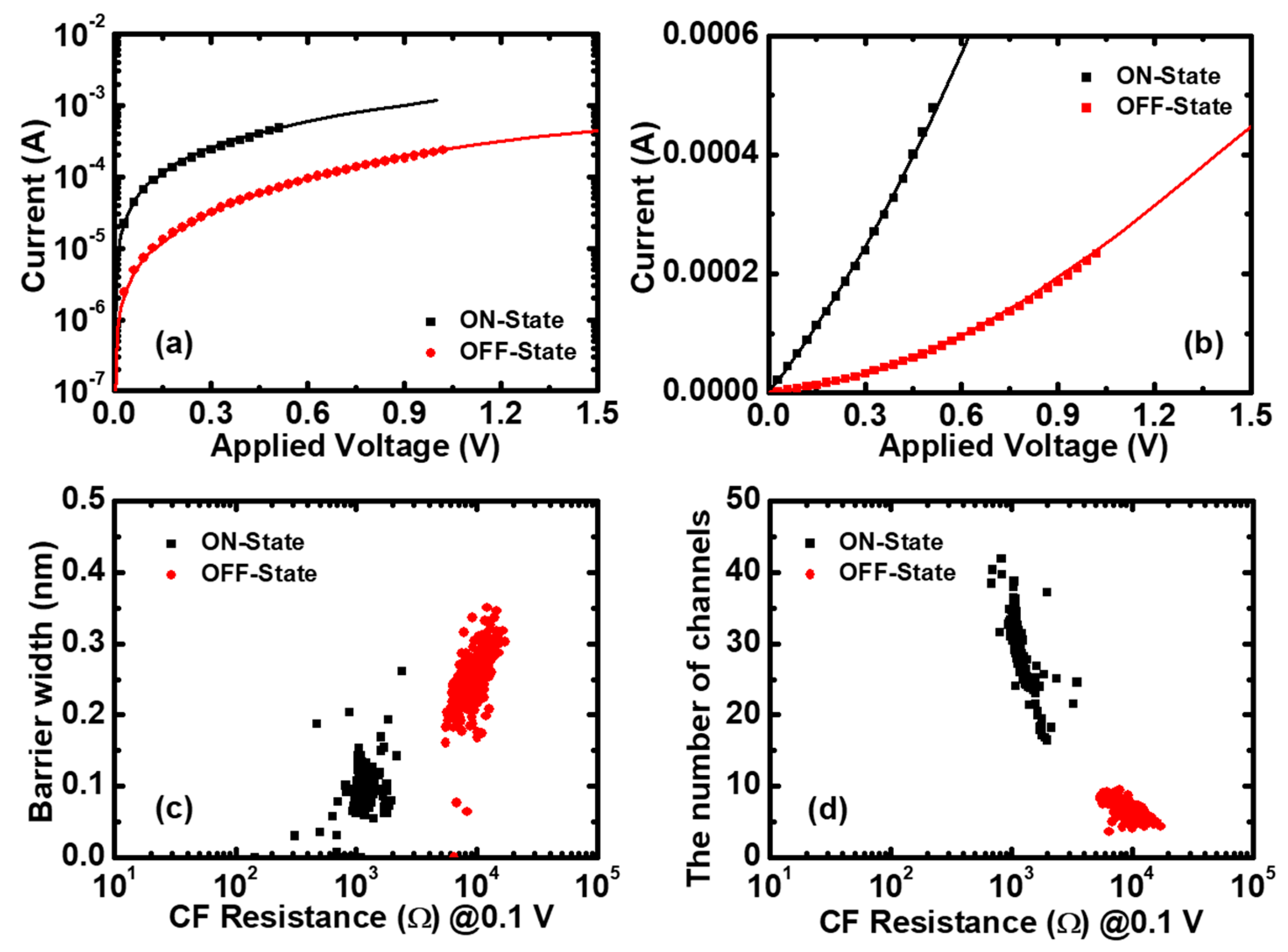
3.2. Quantum Point Contact Model
Many different conduction models have been proposed for the HRS, including Schottky emission [41,42,43,44], trap-assisted tunneling [45,46,47], Poole–Frenkel conduction [43,48], space-charge limited current [49,50,51,52], thermally activated hopping [53,54], and the Quantum Point Contact model (QPC) [55,56,57,58,59,60,61], among others. Specifically, the QPC model can provide a smooth transition from tunneling in the HRS to Ohmic conduction in the LRS for several kinds of RS devices [58,59,60,61]. To analyze the conductive mechanisms of RS processes for Pt/Pt:SiOx/Ta memristors, the QPC model has been introduced here to fit the I–V curves in both the Reset and Set processes.
The QPC model is based on the Landauer transmission approach to calculate conduction along narrow microscopic constrictions [57,58]. According to the Landauer’s approach, the current flowing through a CF with paths can be calculated as [62]:
where is the Fermi–Dirac distribution function, is the energy, is the transmission probability, is the averaged asymmetry parameter (with the constraint ), and is the applied voltage assumed to drop at the cathode and anode interfaces with a fraction of and (1 − ), respectively. Assuming an inverted parabolic potential barrier, we can obtain an expression for the tunneling probability [63,64,65], , where is the barrier height, is related to the inverse of the potential barrier curvature, is the effective electron mass, and is the barrier width at the equilibrium Fermi energy, assumed to be equal to . Inserting the tunneling probability into Equation (3), we can obtain:
There are four parameters in Equation (4). In order to simplify the fitting process, here we fixed and by considering the asymmetry structure of the devices. Then, we extracted the number of CF paths N and the average from the fitting experimental data of 400 cycles by using Equation (4) and the least squares estimation (LSE) method. The I–V fitting results are excellent in both log and linear scales, as shown in Figure 5a,b. Furthermore, Figure 5c,d shows the exacted QPC parameters versus the CF resistance. It can be seen that the average is approximately 0.1 nm the in LRS (ON-state) and 0.25 nm in the HRS (OFF-state), and the average number of CF paths is about 30 in the LRS and five in the HRS.
4. Discussion
According to the screening of the statistical data into different resistance ranges, the distributions of RS parameters were shown to be compatible with a Weibull distribution. After using the Weibull distribution function to fit the experimental data of RS parameters into different resistance ranges, we can obtain that is independent of and is inversely proportional to whereas is proportional to and is independent of , which are consistent with the experimental results. Besides, the Weibull slopes of , , , and are nearly independent of the initial resistances, which means that there are no microstructure variations of the CFs before the Reset and Set points. Furthermore, the QPC model has been validated to account for the conductive mechanism and further show the evolution of the CFs during RS processes. From the LRS to HRS, the number of CF paths would decrease, while the barrier gap would increase.
Combining the fitting results of the QPC model with the statistics of RS parameters, we now try to propose the conductive mechanisms of RS processes. During the ON switching, the RS process is mainly driven by an applied electric field, and the CFs are more likely to grow along the locations of Pt nanostructures. Cation migration and metallic CF formation in RS layers can be identified as a candidate RS mechanism due to the abrupt increase of the current in I–V curves (Figure 1a) [66,67]. During the OFF switching, cations are driven out of the CFs and thus introduce a gap between the CFs and the top Pt electrode. Therefore, the number of CF paths would decrease, while the barrier gap would increase from the LRS to the HRS. The Reset event happens only when the temperature of the CFs reaches a critical value, according to the thermal-activated dissolution model. In addition, according to the statistics, we can know that the variations of the RS parameters can be significantly reduced and the performance of memristors could be improved by controlling the sizes of the CFs before the Reset and Set transitions. That is to say, the variability of RS parameters can be reduced by doping in RS regions, where CFs can be induced to grow along the locations of impurities, or by inserting a two-dimensional material with engineered nanopores, which can modify the RS characteristics of memristors.
Author Contributions
Conceptualization, X.L. and Y.T.; methodology, X.L.; software, X.L.; formal analysis, X.L.; investigation, X.L.; resources, X.L.; data curation, X.L.; writing—original draft preparation, X.L.; writing—review and editing, X.L., X.S., L.L., N.H., X.W., S.S. and Y.T.; visualization, X.L.; supervision, X.L.; project administration, X.L. and Y.T.; funding acquisition, X.L. and Y.T.
Funding
This research was funded in part by the National Natural Science Foundation of China (grant number 61804079), the University Natural Science Foundation of Jiangsu Province (grant number 18KJD510005), the Senior Talent Foundation of Jiangsu Province (grant number SZDG2018007), and the Science Research Funds for Nanjing University of Posts and Telecommunications (grant number NY218110, NY217116).
Acknowledgments
Xiaojuan Lian also thanks the research groups of Feng Miao and J. Joshua Yang for helping with the device’s preparation.
Conflicts of Interest
The authors declare no conflict of interest.
References
- Chua, L.O. Memristor-the missing circuit element. IEEE Trans. Circuit Theory 1971, 18, 507–519. [Google Scholar] [CrossRef]
- Chua, L.O.; Kang, S.M. Memristive devices and systems. Proc. IEEE 1976, 64, 209–223. [Google Scholar] [CrossRef]
- Waser, R.; Aono, M. Nanoionics-Based Resistive Switching Memories. Nat. Mater. 2007, 6, 833–840. [Google Scholar] [CrossRef] [PubMed]
- Strukov, D.B.; Snider, G.S.; Stewart, D.R.; Williams, R.S. The missing memristor found. Nature 2008, 453, 80–83. [Google Scholar] [CrossRef] [PubMed]
- Sawa, A. Resistive switching in transition metal oxides. Mater. Today 2008, 11, 28–36. [Google Scholar] [CrossRef]
- Chua, L.O. Resistance switching memories are memristors. Appl. Phys. A Mater. Sci. Process. 2011, 102, 765–783. [Google Scholar] [CrossRef] [Green Version]
- Yang, J.J.; Pickett, M.D.; Li, X.; Ohlberg, D.A.A.; Stewart, D.R.; Williams, R.S. Memristive switching mechanism for metal/oxide/metal nanodevices. Nat. Nanotechnol. 2008, 3, 429–433. [Google Scholar] [CrossRef]
- Wong, H.-S.P.; Lee, H.-Y.; Yu, S.; Chen, Y.-S.; Wu, Y.; Chen, P.-S.; Lee, B.; Chen, F.T.; Tsai, M.-J. Metal–Oxide RRAM. Proc. IEEE 2012, 100, 1951–1970. [Google Scholar] [CrossRef]
- Xia, Q.F.; Robinett, W.; Cumbie, M.W.; Banerjee, N.; Cardinali, T.J.; Yang, J.J.; Wu, W.; Li, X.M.; Tong, W.M.; Strukov, D.B.; et al. Memristor-CMOS hybrid integrated circuits for reconfigurable logic. Nano Lett. 2009, 9, 3640–3645. [Google Scholar] [CrossRef]
- Jo, S.H.; Chang, T.; Ebong, I.; Bhadviya, B.B.; Mazumder, P.; Lu, W. Nanoscale memristor device as synapse in neuromorphic systems. Nano Lett. 2010, 10, 1297–1301. [Google Scholar] [CrossRef] [PubMed]
- Lee, M.-J.; Lee, C.B.; Lee, D.; Lee, S.R.; Chang, M.; Hur, J.H.; Kim, Y.-B.; Kim, C.-J.; Seo, D.H.; Seo, S.; et al. A fast, high-endurance and scalable non-volatile memory device made from asymmetric Ta2O5−x/TaO2−x bilayer structures. Nat. Mater. 2011, 10, 625–630. [Google Scholar] [CrossRef]
- Chen, W.; Fang, R.; Balaban, M.B.; Yu, W.; Velo, Y.G.; Barnaby, H.J.; Kozicki, M.N. A CMOS-compatible electronic synapse device based on Cu/SiO2/W programmable metallization cells. Nanotechnology 2016, 27, 255202. [Google Scholar] [CrossRef] [PubMed]
- Burgt, Y.; Lubberman, E.; Fuller, E.J.; Keene, S.T.; Faria, G.C.; Agarwal, S.; Marinella, M.J.; Talin, A.A.; Salleo, A. A non-volatile organic electrochemical device as a low-voltage artificial synapse for neuromorphic computing. Nat. Mater. 2017, 16, 414–418. [Google Scholar] [CrossRef]
- Hu, M.; Graves, C.E.; Li, C.; Li, Y.; Ge, N.; Montgomery, E.; Davila, N.; Jiang, H.; Williams, R.S.; Yang, J.; et al. Memristor-Based Analog Computation and Neural Network Classification with a Dot Product Engine. Adv. Mater. 2018, 30, 1705914. [Google Scholar] [CrossRef] [PubMed]
- Li, C.; Belkin, D.; Li, Y.; Yan, P.; Hu, M. Efficient and self-adaptive in-situ learning in multilayer memristor neural networks. Nat. Commun. 2018, 9, 2385. [Google Scholar] [CrossRef] [PubMed]
- Gavrilov, D.; Strukov, D.; Likharev, K.K. Capacity, Fidelity, and Noise Tolerance of Associative Spatial-Temporal Memories Based on Memristive Neuromorphic Networks. Front. Neurosci. 2018, 12, 195. [Google Scholar] [CrossRef] [PubMed]
- Bayat, F.M.; Prezioso, M.; Chakrabarti, B.; Nili, H.; Kataeva, I.; Strukov, D. Implementation of multilayer perceptron network with highly uniform passive memristive crossbar circuits. Nat. Commun. 2017, 9, 2331. [Google Scholar] [CrossRef]
- Li, D.; Wu, B.; Zhu, X.; Wang, J.; Ryu, B.; Lu, W.D.; Lu, W.; Liang, X. MoS2 Memristors Exhibiting Variable Switching Characteristics towards Bio-Realistic Synaptic Emulation. ACS Nano 2018, 9, 9240–9252. [Google Scholar] [CrossRef]
- Zhu, X.; Lu, W.D. Optogenetics-Inspired Tunable Synaptic Functions in Memristors. ACS Nano 2018, 12, 1242–1249. [Google Scholar] [CrossRef]
- Shi, Y.; Liang, X.; Yuan, B.; Chen, V.; Li, H.; Hui, F.; Yu, Z.; Yuan, F.; Pop, E.; Wong, H.-S.P.; et al. Electronic synapses made of layered two-dimensional materials. Nat. Electron. 2018, 1, 458–465. [Google Scholar] [CrossRef]
- Zhao, Y.; Jiang, J.; Nanosci, J. Electronic synapses made of layered two-dimensional materials. Nanotechnol 2018, 18, 8003. [Google Scholar]
- Park, M.H.; Lee, Y.H.; Mikolajick, T.; Schroeder, U.; Hwang, C.S. Review and Perspective on Ferroelectric HfO2-based Thin Films for Memory Applications. MRS Commun. 2018, 8, 795–808. [Google Scholar] [CrossRef]
- Li, Y.; Han, K.; Kang, Y.; Kong, E.Y.J.; Gong, X. Extraction of Polarization-dependent Damping Constant for Dynamic Evaluation of Ferroelectric Films and Devices. IEEE Electron. Device Lett. 2018, 39, 1211–1214. [Google Scholar] [CrossRef]
- Li, Y.; Kang, Y.; Gong, X. Evaluation of Negative Capacitance Ferroelectric MOSFET for Analog Circuit Applications. IEEE Trans. Electron. Devices 2017, 64, 4317–4321. [Google Scholar] [CrossRef]
- Bricalli, A.; Ambrosi, E.; Laudato, M.; Maestro, M.; Rodriguez, R.; Lelmini, D. Resistive Switching Device Technology Based on Silicon Oxide for Improved ON-OFF Ratio—Part II: Select Devices. IEEE Trans. Electron. Devices 2018, 65, 122–128. [Google Scholar] [CrossRef]
- Liu, C.; Lin, C.; Liu, S.; Bai, C.; Zhang, Y. Improvement of switching uniformity in Cu/SiO2/Pt resistive memory achieved by voltage prestress. Jpn. J. Appl. Phys. 2015, 54, 031801. [Google Scholar] [CrossRef]
- Liu, C.; Huang, J.; Lai, C.; Lin, C. Influence of embedding Cu nano-particles into a Cu/SiO2/Pt structure on its resistive switching. Nanoscale Res. Lett. 2013, 8, 156. [Google Scholar] [CrossRef]
- Nandakumar, S.R.; Minvielle, M.; Nagar, S.; Dubourdieu, C.; Rajendran, B. A 250 mV Cu/SiO2/W Memristor with Half-Integer Quantum Conductance States. Nano Lett. 2016, 16, 1602–1608. [Google Scholar] [CrossRef]
- Mehonic, A.; Shluger, A.L.; Gao, D.; Valov, I.; Miranda, E.; Ielmini, D.; Bricalli, A.; Ambrosi, E.; Li, C.; Yang, J.J.; et al. Silicon Oxide (SiOx): A Promising Material for Resistance Switching? Adv. Mater. 2018, 30, 1801187. [Google Scholar] [CrossRef]
- Ng, W.H.; Mehonic, A.; Buckwell, M.; Montesi, L.; Kenyon, A.J. High-Performance Resistance Switching Memory Devices Using Spin-On Silicon Oxide. IEEE Trans. Nanotechnol. 2018, 17, 884–888. [Google Scholar] [CrossRef]
- Munde, M.S.; Mehonic, A.; Ng, W.H.; Buckwell, M.; Montesi, L.; Bosman, M.; Shluger, A.L.; Kenyon, A.J. Intrinsic Resistance Switching in Amorphous Silicon Suboxides: The Role of Columnar Microstructure. Sci. Rep. 2017, 7, 9274. [Google Scholar] [CrossRef] [PubMed]
- Mehonic, A.; Buckwell, M.; Montesi, L.; Munde, M.S.; Gao, D.; Hudziak, S.; Chater, R.J.; Fearn, S.; McPhail, D.; Bosman, M.; et al. Nanoscale Transformations in Metastable, Amorphous, Silicon-Rich Silica. Adv. Mater. 2016, 28, 7486–7493. [Google Scholar] [CrossRef] [PubMed] [Green Version]
- Tappertzhofen, S.; Valov, I.; Tsuruoka, T.; Hasegawa, T.; Waser, R.; Aono, M. Generic Relevance of Counter Charges for Cation-Based Nanoscale Resistive Switching Memories. ACS Nano 2013, 7, 6396–6402. [Google Scholar] [CrossRef] [PubMed]
- Tsuruoka, T.; Terabe, K.; Hasegawa, T.; Valov, I.; Waser, R.; Aono, M. Effects of Moisture on the Switching Characteristics of Oxide-Based, Gapless-Type Atomic Switches. Adv. Funct. Mater. 2012, 22, 70–77. [Google Scholar] [CrossRef]
- Yang, Y.; Gao, P.; Li, L.; Pan, X.; Tappertzhofen, S.; Choi, S.; Waser, R.; Valov, I.; Lu, W.D. Electrochemical dynamics of nanoscale metallic inclusions in dielectrics. Nat. Commun. 2014, 5, 4232. [Google Scholar] [CrossRef] [PubMed] [Green Version]
- Choi, B.J.; Torrezan, A.C.; Norris, K.J.; Miao, F.; Strachan, J.P.; Zhang, M.X.; Ohlberg, D.A.; Kobayashi, N.P.; Yang, J.J.; Williams, R.S. Electrical Performance and Scalability of Pt Dispersed SiO2 Nanometallic Resistance Switch. Nano Lett. 2013, 13, 3213–3217. [Google Scholar] [CrossRef]
- Choi, B.J.; Ge, N.; Yang, J.J.; Zhang, M.-X.; Williams, R.S.; Norris, K.J.; Kobayashi, N.P. New materials for memristive switching. IEEE Int. Symp. Circuits Syst. (ISCAS) 2014, 10, 2808–2811. [Google Scholar]
- Lian, X.; Wang, M.; Yan, P.; Yang, J.J.; Miao, F. Reset switching statistics of TaOx-based Memristor. J. Electroceram. 2017, 39, 132–136. [Google Scholar] [CrossRef]
- Long, S.; Lian, X.; Cagli, T.; Ye, C.; Perniola, L.; Miranda, E.; Liu, M.; Sune, J. Cycle-to-Cycle Intrinsic RESET Statistics in HfO2-Based Unipolar RRAM. IEEE Electron. Device Lett. 2013, 34, 623–625. [Google Scholar] [CrossRef]
- Lian, X.; Miao, F.; Wan, X.; Guo, Y.-F.; Tong, Y.; Electroceram, J. Set transition statistics of different switching regimes of TaOx memristor. J. Electroceram. 2019. [Google Scholar] [CrossRef]
- Michalas, L.; Stathopoulos, S.; Khiat, A.; Prodromakis, T. Conduction mechanisms at distinct resistive levels of Pt/TiO2−x/Pt memristors. Appl. Phys. Lett. 2018, 113, 143503. [Google Scholar] [CrossRef]
- Chen, K.-H.; Tsai, T.-M.; Cheng, C.-M.; Huang, S.-J.; Chang, K.-C.; Liang, S.-P.; Young, T.-F. Schottky Emission Distance and Barrier Height Properties of Bipolar Switching Gd:SiOx RRAM Devices under Different Oxygen Concentration Environments. Materials 2017, 11, 43. [Google Scholar] [CrossRef] [PubMed]
- Gul, F. Carrier transport mechanism and bipolar resistive switching behavior of a nano-scale thin film TiO2 memristor. Ceram. Int. 2018, 44, 11417–11423. [Google Scholar] [CrossRef]
- Gismatulin, A.A.; Kruchinin, V.N.; Gritsenko, V.A.; Prosvirin, I.P.; Yen, T.-J.; Chin, A. Charge transport mechanism of high-resistive state in RRAM based on SiOx. Appl. Phys. Lett. 2019, 114, 033503. [Google Scholar] [CrossRef]
- Bersuker, G.; Gilmer, D.C.; Veksler, D.; Kirsch, P.; Vandelli, L.; Padovani, A.; Larcher, L.; McKenna, K.; Shluger, A.; Iglesias, V.; et al. Metal oxide resistive memory switching mechanism based on conductive filament properties. J. Appl. Phys. 2011, 110, 124518. [Google Scholar] [CrossRef]
- Yan, X.; Zhou, Z.; Ding, B.; Zhao, J.; Zhang, Y. Superior resistive switching memory and biological synapse properties based on a simple TiN/SiO2/p-Si tunneling junction structure. J. Mater. Chem. C 2017, 5, 2259–2267. [Google Scholar] [CrossRef]
- Yu, S.; Guan, X.; Wong, H.-S.P. Conduction mechanism of TiN/HfOx/Pt resistive switching memory: A trap-assisted-tunneling model. Appl. Phys. Lett. 2011, 99, 063507. [Google Scholar] [CrossRef]
- Chang, K.-C.; Tsai, T.-M.; Chang, T.-C.; Wu, H.-H.; Chen, J.-H.; Syu, Y.-E.; Chang, G.-W.; Chu, T.-J.; Liu, G.-R.; Su, Y.-T.; et al. Characteristics and Mechanisms of Silicon-Oxide-Based Resistance Random Access Memory. IEEE Electron. Device Lett. 2013, 34, 399–401. [Google Scholar] [CrossRef]
- Kim, K.M.; Choi, B.J.; Shin, Y.C.; Choi, S.; Hwang, C.S. Anode-interface localized filamentary mechanism in resistive switching of TiO2 thin films. Appl. Phys. Lett. 2007, 91, 012907. [Google Scholar] [CrossRef]
- Hsieh, W.-K.; Lam, K.-T.; Chang, S.-J. Characteristics of tantalum-doped silicon oxide-based resistive random access memory. Mater. Sci. Semicond. Process. 2014, 27, 293–296. [Google Scholar] [CrossRef]
- Sun, C.; Lu, S.M.; Jin, F.; Mo, W.Q.; Song, J.L.; Dong, K.F. The Resistive Switching Characteristics of TiN/HfO2/Ag RRAM Devices with Bidirectional Current Compliance. J. Electron. Mater. 2019, 48, 2992–2999. [Google Scholar] [CrossRef]
- Liu, M.; Abid, Z.; Wang, W.; He, X.; Liu, Q.; Guan, W. Multilevel resistive switching with ionic and metallic filaments. Appl. Phys. Lett. 2009, 94, 233106. [Google Scholar] [CrossRef] [Green Version]
- Kunchur, M.N.; Liang, M.; Gurevich, A. Thermally activated dynamics of spontaneous perpendicular vortices tuned by parallel magnetic fields in thin superconducting films. Phys. Rev. B 2012, 86, 024521. [Google Scholar] [CrossRef]
- Graves, C.E.; Dávila, N.; Merced-Grafals, E.J.; Lam, S.-T.; Strachan, J.P.; Williams, R.S. Temperature and field-dependent transport measurements in continuously tunable tantalum oxide memristors expose the dominant state variable. Appl. Phys. Lett. 2017, 110, 123501. [Google Scholar] [CrossRef]
- Miranda, E.; Mehonic, A.; Ng, W.H.; Kenyon, A.J. Simulation of Cycle-to-Cycle Instabilities in SiOx- Based ReRAM Devices Using a Self-Correlated Process with Long-Term Variation. IEEE Electron. Device Lett. 2018, 40, 28–31. [Google Scholar] [CrossRef]
- Holloway, G.W.; Ivanov, O.; Gavrilov, R.; Bluschke, A.G.; Hold, B.K.; Baugh, J. Electrical Breakdown in Thin Si Oxide Modeled by a Quantum Point Contact Network. IEEE Trans. Electron. Devices 2016, 63, 3005–3010. [Google Scholar] [CrossRef]
- Sune, J.; Miranda, E.; Nafria, M.; Aymerich, X. Point contact conduction at the oxide breakdown of MOS devices. In Proceedings of the International Electron Devices Meeting 1998, Technical Digest (Cat. No.98CH36217), San Francisco, CA, USA, 6–9 December 1998. [Google Scholar]
- Sune, J.; Miranda, E. Understanding soft and hard breakdown statistics, prevalence ratios and energy dissipation during breakdown runaway. In Proceedings of the International Electron Devices Meeting, Technical Digest (Cat. No.01CH37224), Washington, DC, USA, 2–5 December 2001. [Google Scholar]
- Lian, X.; Cartoixà, X.; Miranda, E.; Perniola, L.; Rurali, R.; Long, S.; Liu, M.; Suñé, J. Multi-scale quantum point contact model for filamentary conduction in resistive random access memories devices. J. Appl. Phys. 2014, 115, 244507. [Google Scholar] [CrossRef]
- Zhang, M.; Long, S.; Wang, G.; Xu, X.; Li, Y.; Liu, Q.; Lv, H.; Lian, X.; Miranda, E.; Suñé, J.; et al. Set statistics in conductive bridge random access memory device with Cu/HfO2/Pt structure. Appl. Phys. Lett. 2014, 105, 193501. [Google Scholar] [CrossRef]
- Lian, X.; Wang, M.; Rao, M.; Yan, P.; Yang, J.J.; Miao, F. Characteristics and transport mechanisms of triple switching regimes of TaOx memristor. Appl. Phys. Lett. 2017, 110, 173504. [Google Scholar] [CrossRef]
- Datta, S. Electronic Transport in Mesoscopic Systems; University of Cambridge: Cambridgeshire, UK, 1997. [Google Scholar]
- Buttiker, M. Quantized transmission of a saddle-point constriction. Phys. Rev. B 1990, 41, 7906. [Google Scholar] [CrossRef]
- Bogachek, E.N.; Scherbakov, A.G.; Landman, U. Nonlinear magnetoconductance of nanowires. Phys. Rev. B 1997, 56, 14917. [Google Scholar] [CrossRef]
- Miranda, E.; Sune, J. From post-breakdown conduction to resistive switching effect in thin dielectric films. In Proceedings of the 2012 IEEE International Reliability Physics Symposium (IRPS), Anaheim, CA, USA, 15–19 April 2012; p. 367. [Google Scholar]
- Lübben, M.; Valov, I. Active Electrode Redox Reactions and Device Behavior in ECM Type Resistive Switching Memories. Adv. Electron. Mater. 2019, 1800933. [Google Scholar] [CrossRef]
- Valov, I.; Luebben, M.; Wedig, A.; Waser, R. Mobile Ions, Transport and Redox Processes in Memristive Devices. ECS Trans. 2016, 75, 27–39. [Google Scholar] [CrossRef]
Figure 1.
The Current–Voltage (I–V) characteristics in Pt/Pt:SiOx/Ta memristors. (a) The I–V curves for the Set and Reset transitions. A current compliance limit of 0.5 mA is given in the Set process to avoid the breakdown; (b) The ON and OFF resistance states in 400 cycles, extracted at low voltage (0.1 V).
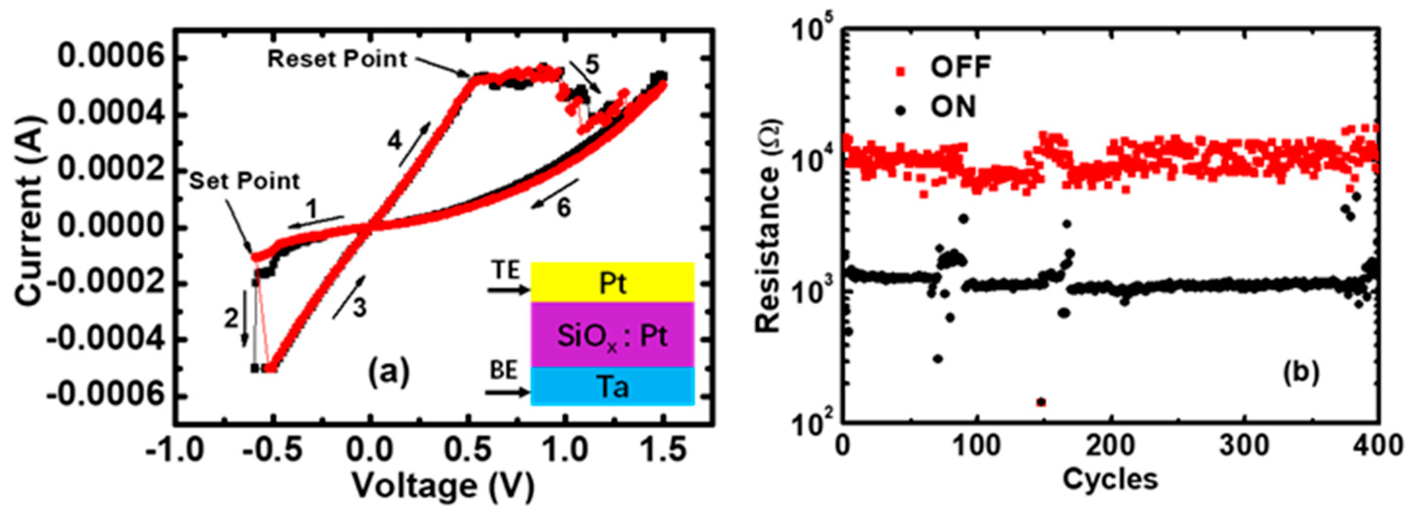
Figure 2.
The statistics of resistance switching (RS) parameters in Pt/Pt:SiOx/Ta memristors. (a) The Reset voltages and (b) the Reset currents versus the ON-state resistances for the measured 400 cycling data of the same device. (c) The Set voltages and (d) the Set currents versus the OFF-state resistances for the measured 400 cycling data of the same device.

Figure 3.
The Weibull distributions of the Reset voltage and the Reset current in Pt/Pt:SiOx/Ta devices. Experimental distributions (symbols) and the fitting to Weibull distribution (lines) of (a) the Reset voltage and (b) the Reset current as functions of the ON-state resistance. Weibull slopes and scale factors of (c) the Reset voltage and (d) the Reset current versus <>, where <> is the average value of the ON-state resistance () in each screening range. It can be seen that the Weibull slopes of the Reset voltage and the Reset current are independent of <>, and the scale factor of the Reset voltage is constant, whereas the Reset current is inversely proportional to <>.
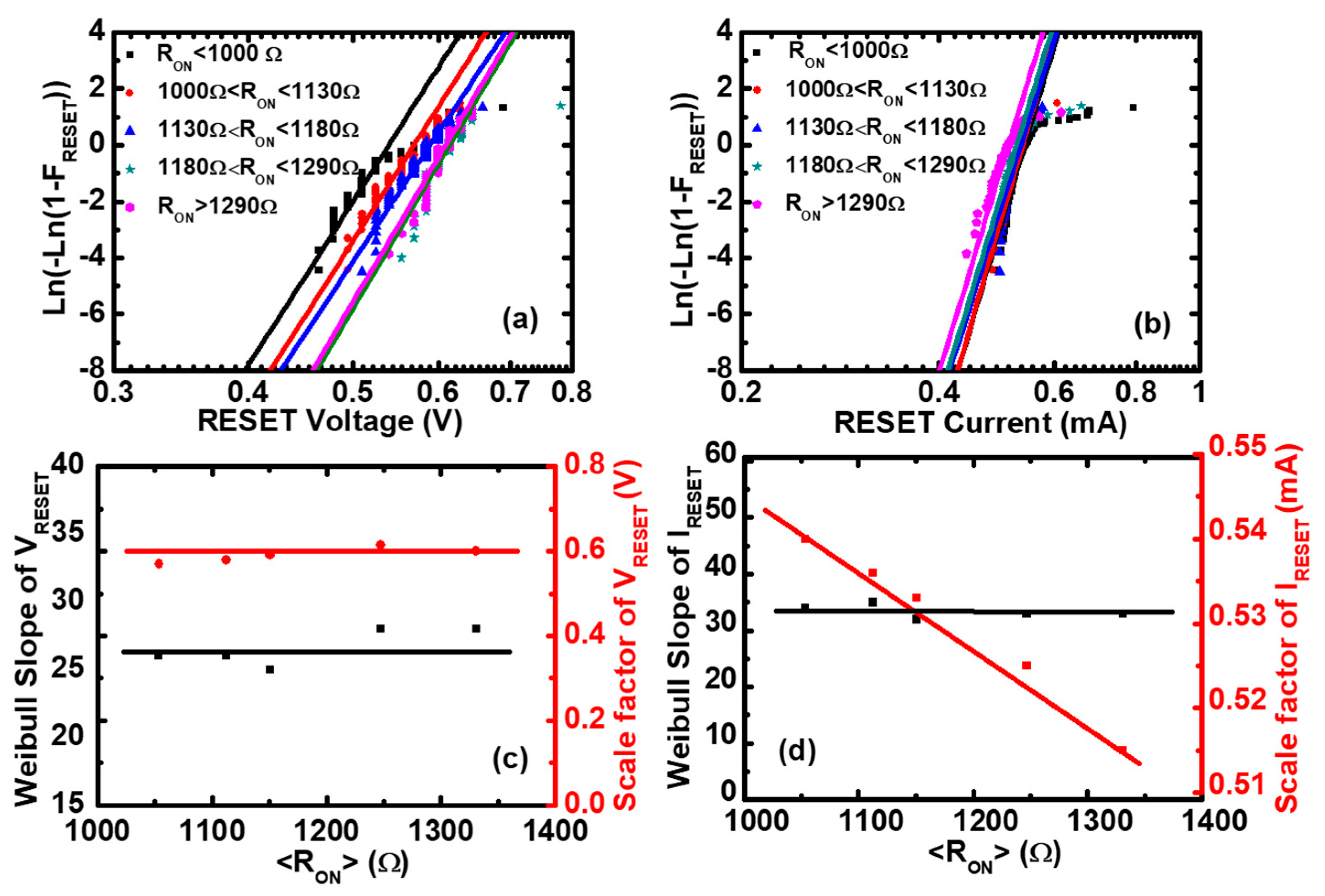
Figure 4.
The Weibull distributions of the Set voltage and the Set current in Pt/Pt:SiOx/Ta devices. Experimental distributions (symbols) and the fitting to Weibull distribution (lines) of (a) the Set voltage and (b) the Set current as functions of the OFF-state resistance. Weibull slopes and scale factors of (c) the Set voltage and (d) the Set current versus <>, where <> is the average value of the OFF-state resistance () in each screening range. It can be seen that the Weibull slopes of the Set voltage and the Set current are independent of <>, and the scale factor of the Set voltage is proportional to <>, whereas the Set current is constant.
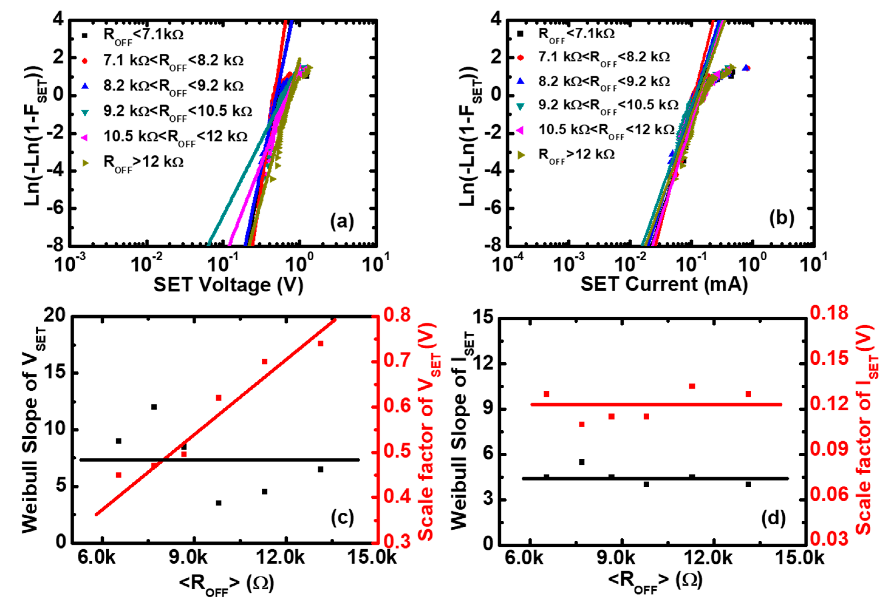
Figure 5.
The quantum points contact (QPC) model applied to Pt/Pt:SiOx/Ta memristors. The I–V fitting results together with experimental data of ON and OFF states (a) in log scale and (b) linear scale. (c) The barrier thickness and (d) the number of CF paths versus the initial resistance, respectively. The averaged values are: in the ON-state; and in the OFF-state.
© 2019 by the authors. Licensee MDPI, Basel, Switzerland. This article is an open access article distributed under the terms and conditions of the Creative Commons Attribution (CC BY) license (http://creativecommons.org/licenses/by/4.0/).
Share and Cite
MDPI and ACS Style
Lian, X.; Shen, X.; Lu, L.; He, N.; Wan, X.; Samanta, S.; Tong, Y. Resistance Switching Statistics and Mechanisms of Pt Dispersed Silicon Oxide-Based Memristors. Micromachines 2019, 10, 369. https://doi.org/10.3390/mi10060369
AMA Style
Lian X, Shen X, Lu L, He N, Wan X, Samanta S, Tong Y. Resistance Switching Statistics and Mechanisms of Pt Dispersed Silicon Oxide-Based Memristors. Micromachines. 2019; 10(6):369. https://doi.org/10.3390/mi10060369
Chicago/Turabian StyleLian, Xiaojuan, Xinyi Shen, Liqun Lu, Nan He, Xiang Wan, Subhranu Samanta, and Yi Tong. 2019. "Resistance Switching Statistics and Mechanisms of Pt Dispersed Silicon Oxide-Based Memristors" Micromachines 10, no. 6: 369. https://doi.org/10.3390/mi10060369
Note that from the first issue of 2016, this journal uses article numbers instead of page numbers. See further details here.