Article

Effect of Annealing Temperature for Ni/AlOx/Pt RRAM Devices Fabricated with Solution-Based Dielectric

1
Department of Electrical and Electronic Engineering, Xi’an Jiaotong-Liverpool University, Suzhou 215123, China
2
Department of Electrical Engineering and Electronics, University of Liverpool, Liverpool L69 3BX, UK
3
School of Electronic and Information Engineering, Xi’an Jiaotong University, Xi’an 710061, China
4
Department of Chemistry, Xi’an Jiaotong-Liverpool University, Suzhou 215123, China
5
Department of Chemistry, University of Liverpool, Liverpool L69 3BX, UK
*
Author to whom correspondence should be addressed.
Micromachines 2019, 10(7), 446; https://doi.org/10.3390/mi10070446
Submission received: 10 May 2019 / Revised: 25 June 2019 / Accepted: 28 June 2019 / Published: 2 July 2019

Abstract

:
Resistive random access memory (RRAM) devices with Ni/AlOx/Pt-structure were manufactured by deposition of a solution-based aluminum oxide (AlOx) dielectric layer which was subsequently annealed at temperatures from 200 °C to 300 °C, in increments of 25 °C. The devices displayed typical bipolar resistive switching characteristics. Investigations were carried out on the effect of different annealing temperatures for associated RRAM devices to show that performance was correlated with changes of hydroxyl group concentration in the AlOx thin films. The annealing temperature of 250 °C was found to be optimal for the dielectric layer, exhibiting superior performance of the RRAM devices with the lowest operation voltage (<1.5 V), the highest ON/OFF ratio (>104), the narrowest resistance distribution, the longest retention time (>104 s) and the most endurance cycles (>150).

1. Introduction

As one of the promising candidates for next-generation nonvolatile memories, resistive random access memory (RRAM) has received considerable attention due to significant advantages concerning simplicity of structure, low power consumption, fast read & write speed, high scalability and 3-D integration feasibility compared to the industry standard silicon-based flash memories [1,2,3,4,5,6,7]. Current candidate materials for the resistive switching (RS) layer of RRAM devices include perovskite, ferromagnetic and metal oxide-based materials [1,3,4,5,8,9,10,11]. In particular, metal oxide-based materials such as AlOx, NiOx, TiOx and HfOx are currently extensively discussed because of the simplicity of the material [10,12,13,14]. Among these materials, AlOx has been widely applied in gate insulator layers [15,16,17,18] and has attracted extensive attention in the RRAM field owing to its wide band gap (~8.9 eV), high thermal stability with Si and Pt, high dielectric constant (~8) and large breakdown electric field [10,14,19,20,21,22] as Kim et al. has reported [19,20,23,24,25,26]. In addition, the superior elasticity [27] and high toughness [28] make it possible for AlOx to be applied under various conditions including vibration and pressure environments [29,30,31]. Cano et al. reported that AlOx-based dielectric layer showed superior stability under environments with hydrofluoric acid pressure [29] and Choi et al. reported large-scale flexible electronics application with AlOx thin film [31], which have demonstrated that the AlOx thin film has great potential as a metal oxide layer in RRAM devices.
A number of fabrication methods for incorporation of a metal oxide RS layer in AlOx-based RRAM devices have been investigated. Methods based on solution processes for metal oxide thin films have been extensively considered, namely spin [32,33,34] and dip coating [35,36,37], drop casting [34,36,37,38] and different printing methods. Compared with traditional fabrication methods such as atomic-layer-deposition (ALD) [17,39,40] and magnetron sputtering [28,40,41], the solution-based method has advantages of low fabrication cost with the elimination of vacuum deposition processes [42], ease of preparation for precursor materials [39,43,44] and high efficiency of device throughput [27], which reveals the promising prospect of solution-based methods in RS layer fabrication. Several factors including plasma cleaning time, deposition gaseous environment and annealing temperature are considered to influence the performance of solution-based metal oxide thin films. A limited number of investigations have been reported regarding the relationship between annealing temperature and performance of RRAM device with solution-based RS layer [10,38].
In this work, the AlOx thin film was deposited with a spin-coating method and then annealed at temperatures of 200 °C to 300 °C, in increments of 25 °C. The RRAM devices with solution-based AlOx thin film were characterized electrically in terms of operation voltage, ON/OFF ratio between the high resistance state (HRS) and low resistance state (LRS), resistance distribution, retention time and endurance cycles. X-ray photoelectron spectroscopy (XPS) results indicate that these performance metrics are associated with different gradients of hydroxyl group (-OH) concentrations in the AlOx thin films with different annealing temperatures. Devices with AlOx thin films annealed at 250 °C demonstrated superior performance with the lowest operation voltage (<1.5 V), the highest ON/OFF ratio (>104), the narrowest resistance distribution, the longest retention time (>104 s) and the most endurance cycles (>150).

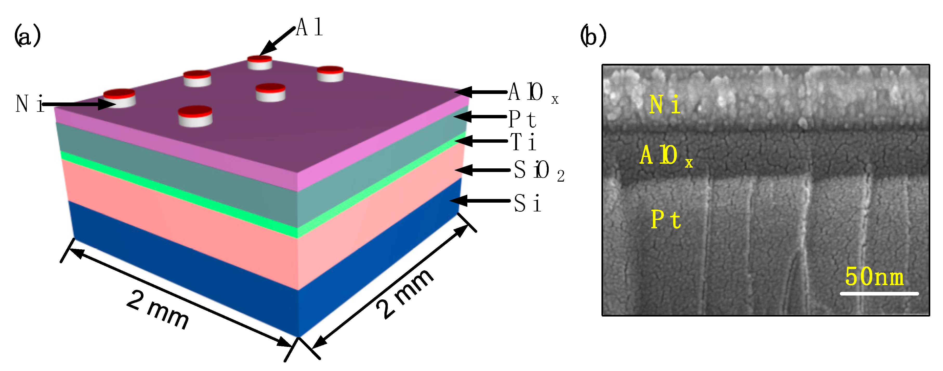
2. Device Fabrication

The fabricated Ni(top)/AlOx/Pt(bottom) memory device structure with dimensions 2 mm × 2 mm is shown in Figure 1a. Firstly, the substrate comprising layers Pt (200 nm)/Ti/SiO2/Si was ultrasonically cleaned in acetone, ethanol and deionized (DI) water, sequentially. Then an aluminum nitrate nonahydrate (Al(NO3)3·9H2O) solution consisting of ~9.353 g Al(NO3)3·9H2O and 10 mL deionized water was prepared as the 2.5 M AlOx precursor. The precursor solution was stirred vigorously for 20 min under ambient air conditions. The Pt substrate surface layer was given a hydrophilic treatment in a plasma cleaner in an atmospheric environment. The AlOx precursor solution, filtered through a 0.45 μm polyether sulfone (PES) syringe, was spin-coated onto the substrate at a spin rate of 4500 rpm for 40 s and subsequently annealed at the different desired temperatures of 200 °C, 225 °C, 250 °C, 275 °C and 300 °C for 60 min under ambient conditions. A ~40 nm-thick top electrode (TE) layer of Ni and a ~40 nm-thick capping layer of Al were both deposited by e-beam evaporation. Figure 1b shows a scanning electron microscope (SEM) cross-sectional image of the device, confirming the target thicknesses of ~40 nm, ~30 nm and ~100 nm for Ni, AlOx and Pt layers respectively.
An Agilent B1500A high-precision semiconductor analyzer (Agilent Santa Rosa, CA, USA) was employed to measure the I-V characteristics with a two-probe configuration. All electrical measurements were performed in the dark and at room temperature within a Faraday cage. In addition, to investigate the effect of annealing temperatures on device performance, X-ray photoelectron spectroscopy (XPS) spectra of constituent Al and O core level (CL) elements were measured.

3. Results and Discussion

3.1. Memoristic Characteristics Based on Al/Ni/Solution-Based AlOx/Pt RRAM

The RRAM devices were operated under 1 mA compliance current (CC) and observed to exhibit typical bipolar RS behavior, as illustrated by the I-V characteristics in Figure 2. The devices with the dielectric layer annealed at 200 °C exhibit typical RRAM breakdown characteristics at very low voltage <0.3 V while breakdown characteristics of 300 °C annealed devices are not usually observed even for voltages higher than 18 V, which is of course, unsuitable for RRAM device application [45,46]. Therefore, RRAM devices with dielectric layers annealed at 225 °C, 250 °C, 275 °C were considered for further evaluation. Compared with unipolar I-V characteristics of other RRAM devices [47], all RRAM devices with Al/Ni/solution-based AlOx/Pt structure demonstrate typical bipolar I-V characteristics without forming operation. The current compliance (CC) is set at 1 mA to prevent catastrophic breakdown of the RRAM devices. During cycling, the HRS was transferred to LRS abruptly in the SET process and the resistance of the LRS began to increase abruptly toward HRS in the RESET process. The SET and RESET process controls the RRAM device transition to ON and OFF states. It is observed that the majority of values of SET voltages (VSET) for the three samples are around 1.5 V while some are up to 4 V. In the RESET process, nearly all RESET voltages (VRESET) are around −1 V approximately. As illustrated in Figure 3, in the SET operation, the average values of VSET are around 3.2 V, 1.0 V and 2.4 V at 225 °C, 250 °C and 275 °C, respectively. RRAM devices with dielectric layer annealed at 250 °C exhibit the lowest SET voltages (Figure 3a) with the highest ON/OFF ratio (>104) between LRS (ON state) and HRS (OFF state). Similar results can be observed in the RESET operation (Figure 3b) although the variation of VRESET average values is not as obvious as that of VSET. Figure 2d shows the cumulative probability for resistance distribution of the RRAM devices annealed at various temperatures. All values of memory resistance at HRS (RHRS) and LRS (RLRS) of consecutive forming-free DC switching cycles were read at 0.1 V. As illustrated in Figure 2d, curves of resistance distribution almost overlap at LRS, indicating that no significant dependence on annealing temperature is apparent at LRS. However, an obvious variation can be observed at RHRS. The uniformity and narrowness of the resistance distribution are key metrics for stability and quality of RRAM devices. A narrow resistance distribution is considered to be a good demonstration of the stability and performance of devices [7,48,49,50]. In this work, the narrowest resistance distribution of Al/Ni/solution-based AlOx/Pt RRAM devices is found for the 250 °C annealing temperature, which therefore presents the best uniformity of the devices.

3.2. Endurance and Retention Properties of Al/Ni/Solution-Based AlOx/Pt RRAM

Figure 4 demonstrates the retention and endurance properties at HRS and LRS for the RRAM devices with RS layers annealed at various temperatures. With the results of resistance distribution above, the resistance values of retention and endurance belong to the range of HRS and LRS values in Figure 2d. Resistance values both at HRS and LRS are read at 0.2 V. Figure 4a–c show DC cycles vs resistance at 1 mA CC of devices annealed at 225 °C, 250 °C and 275 °C, which show similar characteristics to those observed in the resistance distribution of Figure 2d. The best resistance distribution can be observed in 250 °C annealed RRAM devices and the worst uniformity of resistance can be observed in 225 °C annealed RRAM devices. Similarly, the endurance property with the best uniformity is demonstrated in the RRAM device annealed at 250 °C while the worst performance is observed in the RRAM device annealed at 225 °C. The same retention property can be observed in Figure 4d, which shows that the device can sustain data for more than 104 s.
The best performance was found for an annealing temperature of 250 °C with the lowest operation voltage (<1.5 V), the highest ON/OFF ratio (>104), the narrowest resistance distribution, the longest retention time (>104 s) and the most endurance cycles (150).

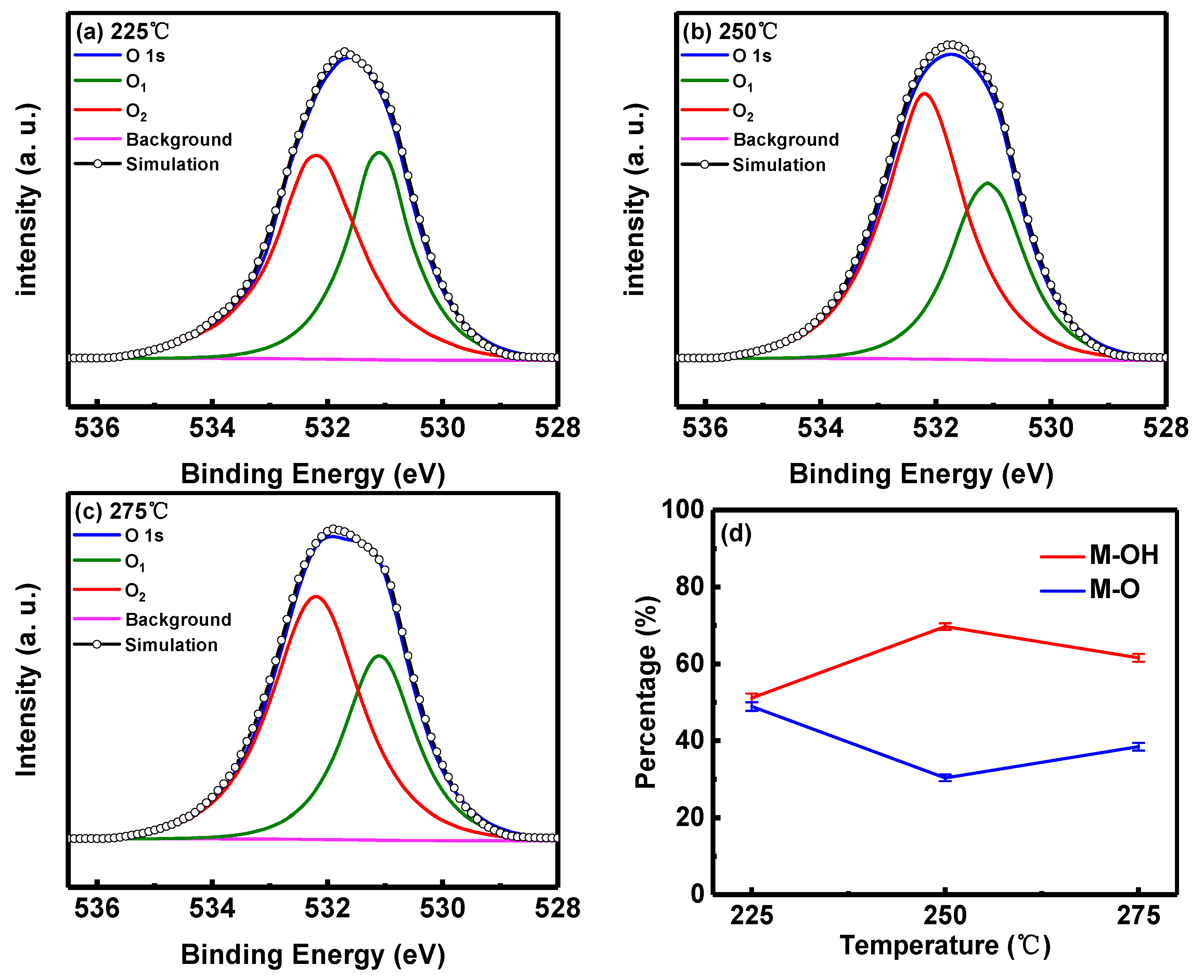
3.3. Switching Mechanism of Al/Ni/Solution-Based AlOx/Pt RRAM

With typical bipolar RS performance demonstrated by Al/Ni/solution-based AlOx/Pt RRAM devices, the RS modeling with fitting curves (250 °C annealed devices) illustrated in Figure 5a is used to investigate the conduction mechanism. Figure 5a shows evidence for space-charge limited current (SCLC) as the dominant conduction mechanism in 250 °C annealed devices. The fitting results show positive and negative bias regions of I-V characteristics in double logarithmic plots. A large area overlap of SET and RESET can be observed due to the approximately equal values of CC and RESET current. The currents are seen to follow Ohmic conduction (I ∝ V) in the low voltage regime [51,52]. At higher bias voltages, the OFF-state slope shows a transition to about 2.0, consistent with Child’ s square law [53,54]. By further increasing the applied voltage, the slope increased to approximately 8.7, again consistent with the SCLC mechanism [53,54,55,56].
Bipolar RS performance of all RRAM devices with different annealing temperatures are considered to be associated with the formation and rupture process of conductive filaments (CF) associated with oxygen vacancies, in the SET/RESET process [2,3,4,15,57]. Figure 5b shows a schematic representation of this process consisting of ON and OFF states, which is considered as the switching mechanism of these devices. The formation and rupture process of CF is associated with the distribution of oxygen ions and oxygen vacancies in the TE and RS layer [22,48,57,58,59]. Figure 5b(i) shows the initial state of RRAM devices without applied voltage, indicating oxygen atoms present in the AlOx thin film. With application of a positive voltage to the Ni electrode in the SET operation, electrons are captured by oxygen atoms in the AlOx thin film [15,27,60,61,62], to yield oxygen ions which drift to TE. The generation process of oxygen ions can be represented as:
O +   2 e     O 2
The oxygen vacancies remain in the AlOx thin film and constitute the dominant components of CF. This formation process of CF consisting of oxygen vacancies in the AlOx thin film is considered to be responsible for the resistance state transition (HRS to LRS) of RRAM devices at the ON state, as depicted in Figure 5b [48,58,60]. Conversely, in the RESET operation, with a negative voltage applied to TE, oxygen ions stored in the electrode drift back to the AlOx thin film under the influence of the negative electrical field and therefore reduce the density of oxygen vacancies in the AlOx thin film [48,63]. This action dominates the rupture process of CF [15,22,48] and the RRAM devices perform at the OFF state (LRS to HRS).
The formation and rupture mechanism of CF is confirmed to be associated with the characteristics of the RS layer in filamentary RRAM devices with the dependency on film thickness, measurement temperature and deposition temperature [64,65,66,67]. In this work, the device performance is found to be dependent on annealing temperature of the dielectric layer and the best performance is observed in the device with a dielectric layer annealed at 250 °C.
Physical characterization was undertaken using XPS. Figure 6a–c show XPS spectra of O 1s core levels for the AlOx thin films annealed at 225 °C, 250 °C and 275 °C. The O 1s CL spectrum can be de-convoluted into two sub-peaks with binding energies located at 531.1 eV (O1) and 532.2 eV (O2) [40,64,65,66,67]. The O1 and O2 peaks are associated with the metal-oxygen bonds (O1) and hydroxyl group (O2), respectively [5,66,67]. As illustrated in Figure 6a–c, the hydroxyl-related peak (O2) increased with annealing temperatures from 225 °C to 250 °C and decreased from 250 °C to 275 °C. Similar behavior has been observed by Xu et al. [68]. The highest and the lowest concentration of the hydroxyl group is found for samples annealed at 250 °C and 225 °C, respectively. Figure 6d shows the integrated intensity of the two sub-peaks referring to the concentration of hydroxyl group (M-OH) and metal-oxygen bonds (M-O) for the three samples. The observed variation in concentration of hydroxyl group has been found to show strong correlation to RRAM device performance. The best performing RRAM device annealed at 250 °C has the highest concentration of hydroxyl group, while the worst performance is observed for device annealed at 225 °C which exhibits the lowest concentration of hydroxyl group.
With the different concentrations of M-O and M-OH in the dielectric layer, two main species of compositions, namely AlOx and Al(OH)x, play dominant roles in switching behavior. We now propose a hypothesis for the relationship between composition and surface roughness of the dielectric layer. The more complex the compositions of the dielectric layer, the higher surface roughness will be present [69,70,71]. The surface roughness assessed by Atomic Force Microscope (AFM) of dielectric layers annealed at 225 °C, 250 °C and 275 °C are 0.682 nm, 0.230 nm and 0.524 nm, respectively. In 225 °C annealed devices, the similar concentration (~50%) of M-O and M-OH can be detected in the film indicating that the concentration of AlOx and Al(OH)x are almost equal. Hence the dielectric layer performance might be affected concurrently by two main compositions. A smooth surface of the dielectric layer is essential to achieve low leakage current and the realization of high-performance dielectric thin films. A higher concentration of M-OH is observed in the 250 °C annealed AlOx thin film, which indicates that Al(OH)x has a more dominant influence on the layer properties. Compared with Al(OH)x, the influence of AlOx is less significant, which results in a lower surface roughness. In addition, the existence of the hydroxyl group in the dielectric layer is associated with water absorption, which affects the permittivity of AlOx with a slight fluctuation (~9.3–~11.5) and hence the capacitance associated with the dielectric thin film. This part will be submitted to further investigation.

4. Conclusions

RRAM devices with Al/Ni/AlOx/Pt structure were fabricated by a solution-based process with the RS layer annealed at 200 °C, 225 °C, 250 °C, 275 °C and 300 °C. The effect on RRAM device performance for annealing temperatures of 225 °C, 250 °C, 275 °C was investigated in terms of the operation voltages of RS characteristics, resistance distribution, endurance cycles and retention uniformity. The worst device performance was observed for an annealing temperature of 225 °C and the better performance was demonstrated in the device annealed at 275 °C. The best performance was found for an annealing temperature of 250 °C with the lowest operation voltage (<1.5 V), the highest ON/OFF ratio (>104), the narrowest resistance distribution, the longest retention time (>104 s) and the most endurance cycles (150), which indicates the lowest energy consumption and the excellent stability of the RRAM devices. An XPS study has been conducted to determine elements present in the AlOx thin films prepared at different annealing temperature with the aim of explaining the variation of associated RRAM devices performance. The device performance was considered to be related to the concentration gradient of hydroxyl groups in the solution-based AlOx thin films for different annealing temperatures.

Author Contributions

Conceptualization, Z.S., Y.Q. and C.Z. (Chun Zhao); Methodology, Z.S., Y.Q. and C.Z. (Chun Zhao); Software, Z.S., Y.Q., T.L. and Y.H.; Validation, Z.S., C.Z. (Chun Zhao), C.Z. (Cezhou Zhao) and S.H.; Formal Analysis, Z.S., Y.Q., I.Z.M., C.Z. (Cezhou Zhao), S.H. and C.Z. (Chun Zhao); Investigation, Z.S. and Y.Q.; Resources, C.Z. (Chun Zhao), C.Z. (Cezhou Zhao) and L.Y.; Data Curation, Z.S., Y.Q., T.L. and Y.H.; Writing-Original Draft Preparation, Z.S., Y.Q. and C.Z. (Chun Zhao); Writing-Review & Editing, Z.S., Y.Q., I.Z.M., C.Z. (Cezhou Zhao), S.H. and C.Z. (Chun Zhao); Visualization, Z.S. and Y.Q.; Supervision, Y.Q., I.Z.M., C.Z. (Cezhou Zhao), S.H. and C.Z. (Chun Zhao); Project Administration, C.Z. (Cezhou Zhao) and C.Z. (Chun Zhao); Funding Acquisition, I.Z.M., C.Z. (Cezhou Zhao) and C.Z. (Chun Zhao).

Funding

This research was funded in part by the National Natural Science Foundation of China (21503169, 2175011441,61704111), Key Program Special Fund in XJTLU (KSF-P-02, KSF-T-03, KSF-A-04, KSF-A-05, KSF-A-07). The author Ivona Z. Mitrovic acknowledges the British Council UKIERI project no. IND/CONT/G/17-18/18.

Conflicts of Interest

The authors declare no conflict of interest.

References

  1. Ambrosi, E.; Bricalli, A.; Laudato, M.; Ielmini, D. Impact of oxide and electrode materials on the switching characteristics of oxide ReRAM devices. Faraday Discuss. 2019, 213, 87–98. [Google Scholar] [CrossRef] [PubMed]
  2. Bang, S.; Kim, M.; Kim, T.; Lee, D.; Kim, S.; Cho, S. Gradual switching and self-rectifying characteristics of Cu/α-IGZO/p+-Si RRAM for synaptic device application. Solid State Electron. 2018, 150, 60–65. [Google Scholar] [CrossRef]
  3. Bertolazzi, S.; Bondavalli, P.; Roche, S.; San, T.; Choi, S. Nonvolatile Memories Based on Graphene and Related 2D Materials. Adv. Mater. 2019, 31, e1806663. [Google Scholar] [CrossRef] [PubMed] [Green Version]
  4. Bukke, R.N.; Avis, C.; Jang, J. Solution-Processed Amorphous In–Zn–Sn Oxide Thin-Film Transistor Performance Improvement by Solution-Processed Y2O3Passivation. IEEE Electron Devices Lett. 2016, 37, 433–436. [Google Scholar] [CrossRef]
  5. Bukke, R.N.; Mude, N.N.; Lee, J.; Avis, C.; Jang, J. Effect of Hf alloy in ZrOx gate insulator for solution processed a-IZTO thin film transistors. IEEE Electron Devices Lett. 2018. [Google Scholar] [CrossRef]
  6. Chen, P.-H.; Su, Y.-T.; Chang, F.-C. Stabilizing Resistive Switching Characteristics by Inserting Indium-Tin-Oxide Layer as Oxygen Ion Reservoir in HfO2-Based Resistive Random Access Memory. IEEE Trans. Electron Dev. 2019, 66, 1276–1280. [Google Scholar] [CrossRef]
  7. Arun, N.; Kumar, K.; Mangababu, A.; Rao, S.; Pathat, A. Influence of the bottom metal electrode and gamma irradiation effects on the performance of HfO2-based RRAM devices. Radiat. Eff. Defects Solids 2019, 174, 66–75. [Google Scholar] [CrossRef]
  8. Cazorla, M.; Aldana, S.; Maestro, M.; Gonzalez, M. Thermal study of multilayer resistive random access memories based on HfO2 and Al2O3 oxides. J. Vac. Sci. Technol. B 2019, 37. [Google Scholar] [CrossRef]
  9. Chen, J.; Yin, C.; Li, Y.; Qin, C. LiSiOx-based Analog Memristive Synapse for Neuromorphic Computing. IEEE Electron Devices Lett. 2019. [Google Scholar] [CrossRef]
  10. Duan, W.; Tang, Y.; Liang, X.; Rao, C.; Chu, J.; Wang, G.; Pei, Y. Solution processed flexible resistive switching memory based on Al-In-O self-mixing layer. J. Appl. Phys. 2018, 124. [Google Scholar] [CrossRef]
  11. Bartlett, P.; Berg, A.I.; Bernasconi, M.; Brown, S.; Burr, G.; Foroutan-Nejad, C.; Gale, E.; Huang, R.; Ielmini, D.; Kissling, G.; et al. Phase-change memories (PCM)-Experiments and modelling: General discussion. Faraday Discuss. 2019, 213, 393–420. [Google Scholar] [CrossRef] [PubMed]
  12. Gao, S.; Yi, X.; Shang, J.; Liu, G.; Li, R.-W. Organic and hybrid resistive switching materials and devices. Chem. Soc. Rev. 2019, 48, 1531–1565. [Google Scholar] [CrossRef] [PubMed]
  13. Han, P.; Lai, T.-C.; Wang, M.; Zhao, X.-R.; Cao, Y.-Q.; Wu, D.; Li, A.-D. Outstanding memory characteristics with atomic layer deposited Ta2O5/Al2O3/TiO2/Al2O3/Ta2O5 nanocomposite structures as the charge trapping layer. Appl. Surf. Sci. 2019, 467–468, 423–427. [Google Scholar] [CrossRef]
  14. He, Z.-Y.; Wang, T.-Y.; Chen, L.; Zhu, H.; Sun, Q.-Q.; Ding, S.-J.; Zhang, D. Atomic Layer-Deposited HfAlOx-Based RRAM with Low Operating Voltage for Computing In-Memory Applications. Nanoscale Res. Lett. 2019, 14, 51. [Google Scholar] [CrossRef] [PubMed]
  15. Tian, M.; Zhong, H. Effects of Electrode on the Performance of Al2O3 Based Metal-Insulator-Metal Antifuse. ECS J. Solid State Sci. Technol. 2019, 8, N32–N35. [Google Scholar] [CrossRef]
  16. Hur, J.H.; Kim, D. A study on mechanism of resistance distribution characteristics of oxide-based resistive memory. Sci. Rep. 2019, 9, 302. [Google Scholar] [CrossRef] [PubMed]
  17. Kadhim, M.S.; Yang, F.; Sun, B.; Hou, W.; Peng, H.; Hou, Y.; Jia, Y.; Yuan, L.; Yu, Y.; Zhao, Y. Existence of Resistive Switching Memory and Negative Differential Resistance State in Self-Colored MoS2/ZnO Heterojunction Devices. ACS Appl. Electron. Mater. 2019, 1, 318–324. [Google Scholar] [CrossRef]
  18. Kang, K.; Ahn, H.; Song, Y.; Lee, W.; Kim, J.; Kim, Y.; Yoo, D.; Lee, T. High-Performance Solution-Processed Organo-Metal Halide Perovskite Unipolar Resistive Memory Devices in a Cross-Bar Array Structure. Adv. Mater. 2019, 31, e1804841. [Google Scholar] [CrossRef]
  19. Kim, G.; Kornijcuk, V.; Kim, D.; Kim, I.; Hwang, C.; Jesong, D. Artificial Neural Network for Response Inference of a Nonvolatile Resistance-Switch Array. Micromachines (Basel) 2019, 10, 219. [Google Scholar] [CrossRef]
  20. Kim, S.; Chen, J.; Chen, Y.C.; Kim, M.H.; Kim, H.; Kwon, M.W.; Hwang, S.; Ismail, M.; Li, Y.; Miao, X.-S.; et al. Neuronal dynamics in HfOx/AlOy-based homeothermic synaptic memristors with low-power and homogeneous resistive switching. Nanoscale 2018, 11, 237–245. [Google Scholar] [CrossRef]
  21. Kim, T.-H.; Kim, S.; Kim, H.; Kim, M. Highly uniform and reliable resistive switching characteristics of a Ni/WOx/p + -Si memory device. Solid State Electron. 2018, 140, 51–54. [Google Scholar] [CrossRef]
  22. Ram, J.; Kumar, R. Effect of Annealing on the Surface Morphology, Optical and and Structural Properties of Nanodimensional Tungsten Oxide Prepared by Coprecipitation Technique. J. Electron. Mater. 2018, 48, 1174–1183. [Google Scholar] [CrossRef]
  23. Kang, X.; Guo, J.; Gao, Y.; Ren, S.; Chen, W. NiO-based resistive memory devices with highly improved uniformity boosted by ionic liquid pre-treatment. Appl. Surf. Sci. 2019, 480, 57–62. [Google Scholar] [CrossRef]
  24. Le, P.Y.; Tran, H.; Zhao, Z.; Mckenzie, D. Tin oxide artificial synapses for low power temporal information processing. Nanotechnology 2019. [Google Scholar] [CrossRef] [PubMed]
  25. Lee, B.R.; Park, J.; Lee, T.; Kim, T. Highly Flexible and Transparent Memristive Devices Using Cross-Stacked Oxide/Metal/Oxide Electrode Layers. ACS. Appl. Mater. Interfaces 2019, 11, 5215–5222. [Google Scholar] [CrossRef] [PubMed]
  26. Lübben, M.; Valov, I. Active Electrode Redox Reactions and Device Behavior in ECM Type Resistive Switching Memories. Adv. Electron. Mater. 2019. [Google Scholar] [CrossRef]
  27. Zhang, R.; Huang, H.; Xia, Q.; Ye, C.; Wei, X. Role of Oxygen Vacancies at the TiO2/HfO2 Interface in Flexible Oxide-Based Resistive Switching Memory. Adv. Electron. Mater. 2019, 5. [Google Scholar] [CrossRef]
  28. Moussa, S.; Mauzeroll, J. Review—Microelectrodes: An Overview of Probe Development and Bioelectrochemistry Applications from 2013 to 2018. J. Electrochem. Soc. 2019, 166, G25–G38. [Google Scholar] [CrossRef]
  29. Cano, A.M.; George, S.; Marquardt, A.; DuMont, D. Effect of HF Pressure on Thermal Al2O3 Atomic Layer Etch Rates and Al2O3 Fluorination. J. Phys. Chem. C 2019, 123, 10346–10355. [Google Scholar] [CrossRef]
  30. Lin, C.-Y.; Wang, J.-C.; Chen, T.-C. Analysis of suspension and heat transfer characteristics of Al2O3 nanofluids prepared through ultrasonic vibration. Appl. Energy 2011, 88, 4527–4533. [Google Scholar] [CrossRef]
  31. Zawrah, M.F.; Khattab, R.M.; Girgis, L.G.; Daidamony, H. Stability and electrical conductivity of water-base Al2O3 nanofluids for different applications. HBRC J. 2019, 12, 227–234. [Google Scholar] [CrossRef]
  32. Wang, H.; Zhang, H.; Liu, J.; Xue, D.; Liang, H. Hydroxyl Group Adsorption on GaN (0001) Surface: First Principles and XPS Studies. J. Electron. Mater. 2019, 48, 2430–2437. [Google Scholar] [CrossRef]
  33. Li, L. Ternary Memristic Effect of Trilayer-Structured Graphene-Based Memory Devices. Nanomaterials (Basel) 2019, 9, 518. [Google Scholar] [CrossRef] [PubMed]
  34. Niu, G.; Calka, P.; Huang, P.; Sharath, S.; Petzold, S.; Gloskovskii, A.; Zhao, Y.; Kang, J. Operando diagnostic detection of interfacial oxygen ‘breathing’ of resistive random access memory by bulk-sensitive hard X-ray photoelectron spectroscopy. Mater. Res. Lett. 2019, 7, 117–123. [Google Scholar] [CrossRef]
  35. Li, L.; Li, G. High-Performance Resistance-Switchable Multilayers of Graphene Oxide Blended with 1,3,4-Oxadiazole Acceptor Nanocomposite. Micromachines (Basel) 2019, 10, 140. [Google Scholar] [CrossRef] [PubMed]
  36. Petzold, S.; Sharath, S.; Lemke, J.; Hildebrandt, E.; Trautmann, C. Heavy Ion Radiation Effects on Hafnium Oxide based Resistive Random Access Memory. IEEE Trans. Nucl. Sci. 2019. [Google Scholar] [CrossRef]
  37. Russo, P.; Xiao, M.; Zhou, N. Electrochemical Oxidation Induced Multi-Level Memory in Carbon-Based Resistive Switching Devices. Sci. Rep. 2019, 9, 1564. [Google Scholar] [CrossRef]
  38. Liu, A.; Noh, Y.-Y.; Zhu, H.; Sun, H.; Xu, Y. Solution Processed Metal Oxide High-kappa Dielectrics for Emerging Transistors and Circuits. Adv. Mater. 2018, e1706364. [Google Scholar] [CrossRef]
  39. Liu, T.; Wu, W.; Liao, K.; Sun, Q.; Gong, X. Fabrication of carboxymethyl cellulose and graphene oxide bio-nanocomposites for flexible nonvolatile resistive switching memory devices. Carbohydr. Polym. 2019, 214, 213–220. [Google Scholar] [CrossRef]
  40. Wu, H.; Yao, P.; Zhao, M.; Liu, Y.; Xi, Y. Reliability Perspective on Neuromorphic Computing Based on Analog RRAM. In Proceedings of the 2019 IEEE International Reliability Physics Symposium (IRPS), Monterey, CA, USA, 23 May 2019. [Google Scholar]
  41. Mao, J.-Y.; Zhou, L.; Ren, Y.; Yang, J.; Chang, C. A bio-inspired electronic synapse using solution processable organic small molecule. J. Mater. Chem. C 2019, 7, 1491–1501. [Google Scholar] [CrossRef]
  42. Nenning, A.; Fleig, J. Electrochemical XPS investigation of metal exsolution on SOFC electrodes: Controlling the electrode oxygen partial pressure in ultra-high-vacuum. Surf. Sci. 2019, 680, 43–51. [Google Scholar] [CrossRef]
  43. Yi, X.; Yu, Z.; Niu, X.; Shang, J.; Mao, G.; Yin, T.; Yang, H.; Xue, W.; Dhanapal, P.; Qu, S.; et al. Intrinsically Stretchable Resistive Switching Memory Enabled by Combining a Liquid Metal-Based Soft Electrode and a Metal-Organic Framework Insulator. Adv. Electron. Mater. 2019, 5. [Google Scholar] [CrossRef]
  44. Yen, T.J.; Wang, X.; Li, J.; Cho, K. All Non metal Resistive Random Access Memory. Sci. Rep. 2019, 9, 6144. [Google Scholar] [CrossRef] [PubMed]
  45. Long, S.; Lian, X.; Cagli, C.; Perniola, L. A Model for the Set Statistics of RRAM Inspired in the Percolation Model of Oxide Breakdown. IEEE Electron Dev. Lett. 2013, 34, 999–1001. [Google Scholar] [CrossRef]
  46. Sun, C.; Lu, S.; Jin, F.; Mo, W.; Song, J.; Dong, K. The Resistive Switching Characteristics of TiN/HfO2/Ag RRAM Devices with Bidirectional Current Compliance. J. Electron. Mater. 2019, 48, 2992–2999. [Google Scholar] [CrossRef]
  47. Chen, Y.-C.; Chen, Y.-F.; Wu, X.; Zhou, F.; Guo, M.; Lin, C.-Y.; Hsieh, C.-C.; Fowler, B.; Chang, T.-C.; Lee, J.; et al. Dynamic conductance characteristics in HfOx-based resistive random access memory. RSC Adv. 2017, 7, 12984–12989. [Google Scholar] [CrossRef]
  48. Qi, Y.; Zhao, C.; Zhao, C.; Xu, W.; Shen, Z.; He, J.; Zhao, T.; Fang, Y.; Liu, Q.; Yi, R.; et al. Enhanced resistive switching performance of aluminum oxide dielectric with a low temperature solution-processed method. Solid State Electron. 2019, 158, 28–36. [Google Scholar] [CrossRef]
  49. Lee, D.; Kim, S.; Cho, K. Integration of 4F2 selector-less crossbar array 2Mb ReRAM based on transition metal oxides for high density memory applications. In Proceedings of the 2012 Symposium on VLSI Technology (VLSIT), Honolulu, HI, USA, 12–14 June 2012. [Google Scholar]
  50. He, Y.; Ma, G.; Zhou, X.; Cai, H.; Liu, C.; Zhang, J.; Wang, H. Impact of chemical doping on resistive switching behavior in zirconium-doped CH3NH3PbI3 based RRAM. Org. Electron. 2019, 68, 230–235. [Google Scholar] [CrossRef]
  51. Chang, Y.-F.; Fowler, B.; Chen, Y.-C.; Chen, Y.-T.; Wang, Y.; Xue, F.; Zhou, F.; Lee, J. Intrinsic SiOx-based unipolar resistive switching memory. II. Thermal effects on charge transport and characterization of multilevel programing. J. Appl. Phys. 2014, 116. [Google Scholar] [CrossRef]
  52. Lin, C.-Y.; Wu, C.-Y.; Wu, C.-Y.; Hu, C.; Tsenga, T.-Y. Bistable Resistive Switching in Al2O3 Memory Thin Films. J. Electrochem. Soc. 2007, 154, 4. [Google Scholar] [CrossRef]
  53. Liu, Z.; Chen, P.; Liu, Y.; Yang, M.; Wong, J.; Cen, Z.; Zhang, S. Temperature-Dependent Charge Transport in Al/Al Nanocrystal Embedded Al2O3 Nanocomposite/p-Si Diodes. ECS Solid State Lett. 2012, 1, Q4–Q7. [Google Scholar] [CrossRef]
  54. Kim, Y.; Ohmi, S.; Tsutsui, K.; Iwai, H. Space-Charge-Limited Currents in La2O3Thin Films Deposited by E-Beam Evaporation after Low Temperature Dry-Nitrogen Annealing. Jpn. J. Appl. Phys. 2005, 44, 4032–4042. [Google Scholar] [CrossRef]
  55. Chuang, K.-C.; Chu, C.; Zhang, H.; Luo, J.; Li, W.; Li, Y. Impact of the Stacking Order of HfOx and AlOx Dielectric Films on RRAM Switching Mechanisms to Behave Digital Resistive Switching and Synaptic Characteristics. IEEE J. Electron Devices Soc. 2019. [Google Scholar] [CrossRef]
  56. Rodrigues, A.N.; Santos, Y.P.; Rodrigues, C.L.; Macedo, M.A. Al2O3 thin film multilayer structure for application in RRAM devices. Solid State Electron. 2018, 149, 1–5. [Google Scholar] [CrossRef]
  57. Rodriguez-Fernandez, A.; Aldana, S.; Campabadalm, F.; Sune, J. Resistive Switching with Self-Rectifying Tunability and Influence of the Oxide Layer Thickness in Ni/HfO2/n+-Si RRAM Devices. IEEE Trans. Electron Dev. 2017, 64, 3159–3166. [Google Scholar] [CrossRef]
  58. Wu, L.; Dong, C.; Wang, X.; Li, J.; Li, M. Annealing effect on the bipolar resistive switching memory of NiZn ferrite films. J. Alloys Compd. 2019, 779, 794–799. [Google Scholar] [CrossRef]
  59. Gao, L.; Li, Y.; Li, Q.; Song, Z.; Ma, F. Enhanced resistive switching characteristics in Al2O3 memory devices by embedded Ag nanoparticles. Nanotechnology 2017, 28, 215201. [Google Scholar] [CrossRef] [PubMed]
  60. Wu, X.; Cha, D.; Bosman, M.; Raghavan, N.; Migas, D.; Borisenko, V.; Zhang, X.; Li, K.; Pey, K. Intrinsic nanofilamentation in resistive switching. J. Appl. Phys. 2013, 113. [Google Scholar] [CrossRef]
  61. Lee, J.; Schell, W.; Zhu, X.; Lu, W. Charge Transition of Oxygen Vacancies during Resistive Switching in Oxide-Based RRAM. ACS. Appl. Mater. Interfaces 2019, 11, 11579–11586. [Google Scholar] [CrossRef]
  62. Sarkar, B.; Lee, B.; Misra, V. Understanding the gradual reset in Pt/Al2O3/Ni RRAM for synaptic applications. Semicond. Sci. Technol. 2015, 30. [Google Scholar] [CrossRef]
  63. Qi, Y.; Zhao, C.; Liu, C.; Fang, Y.; He, J.; Luo, T.; Yang, L.; Zhao, C. Comparisons of switching characteristics between Ti/Al2O3/Pt and TiN/Al2O3/Pt RRAM devices with various compliance currents. Semicond. Sci. Technol. 2018, 33. [Google Scholar] [CrossRef]
  64. Cook, S.; Dylla, M.; Rosenberg, A.; Mansley, Z.; Fong, D. The Vacancy-Induced Electronic Structure of the SrTiO3−δ Surface. Adv. Electron. Mater. 2019, 5. [Google Scholar] [CrossRef]
  65. Lyu, F.; Bai, Y.; Wang, Q.; Wang, L.; Zhang, X.; Yin, Y. Coordination-assisted synthesis of iron-incorporated cobalt oxide nanoplates for enhanced oxygen evolution. Mater. Today Chem. 2019, 11, 112–118. [Google Scholar] [CrossRef]
  66. Mefford, J.T.; Kurilovich, A.; Saunders, J.; Hardin, W.; Abakumov, A.; Forslund, R. Decoupling the roles of carbon and metal oxides on the electrocatalytic reduction of oxygen on La1-xSrxCoO3-delta perovskite composite electrodes. Phys. Chem. Chem. Phys. 2019, 21, 3327–3338. [Google Scholar] [CrossRef] [PubMed]
  67. Sun, B.; Qian, Y.; Liang, Z.; Guo, Y.; Xue, Y.; Tian, J.; Cui, H. Oxygen vacancy-rich BiO2-x ultra-thin nanosheet for efficient full-spectrum responsive photocatalytic oxygen evolution from water splitting. Sol. Energy Mater. Sol. Cells 2019, 195, 309–317. [Google Scholar] [CrossRef]
  68. Xu, W.; Wang, H.; Xie, F.; Chen, J.; Cao, H.; Xu, J. Facile and environmentally friendly solution-processed aluminum oxide dielectric for low-temperature, high-performance oxide thin-film transistors. ACS Appl. Mater. Interfaces 2015, 7, 5803–5810. [Google Scholar] [CrossRef]
  69. Juárez-Moreno, J.A.; Ávila-Ortega, A.; Oliva, A.I.; Avilés, F. Effect of wettability and surface roughness on the adhesion properties of collagen on PDMS films treated by capacitively coupled oxygen plasma. Appl. Surf. Sci. 2015, 349, 763–773. [Google Scholar]
  70. Allahbakhsh, A.; Sharif, F.; Mazinani, S. The Influence of Oxygen-Containing Functional Groups on the Surface Behavior and Roughness Characteristics of Graphene Oxide. Nano 2013, 8. [Google Scholar] [CrossRef]
  71. Boronat, M.; Corma, A.; Illas, F.; Radilla, J. Mechanism of selective alcohol oxidation to aldehydes on gold catalysts: Influence of surface roughness on reactivity. J. Catal. 2011, 278, 50–58. [Google Scholar] [CrossRef]
Figure 1. (a) Schematic of an Al/Ni/solution-based AlOx/Pt RRAM device; (b) a scanning electron microscope (SEM) cross-sectional image of the Al/Ni/solution-based AlOx/Pt RRAM device.
Micromachines 10 00446 g001
Figure 2. I-V curves of Al/Ni/solution-based AlOx/Pt RRAM devices with (resistive switching) RS layer annealed at (a) 225 °C; (b) 250 °C and (c) 275 °C. (d) Resistance distribution of Al/Ni/solution-based AlOx/Pt RRAM device with RS layer deposited at various temperatures.
Micromachines 10 00446 g002
Figure 3. Voltage distribution of (a) SET operation and (b) RESET operation for Al/Ni/solution-based AlOx/Pt RRAM devices with RS layer annealed at different temperatures.
Micromachines 10 00446 g003
Figure 4. Endurance property of Al/Ni/solution-based AlOx/Pt RRAM devices with RS layer annealed at (a) 225 °C; (b) 250 °C and (c) 275 °C. (d) Retention property of RRAM devices annealed at various temperatures.
Micromachines 10 00446 g004
Figure 5. (a) Curve fitting of I-V characteristics for Al/Ni/solution-based AlOx/Pt RRAM devices indicating SCLC conduction. (b) Diagrams to describe the switching mechanism of Al/Ni/solution-based AlOx/Pt RRAM devices at (i) the initial state, (ii) the ON state and (iii) the OFF state, respectively.
Micromachines 10 00446 g005
Figure 6. XPS spectra of O 1s CLs for Al/Ni/solution-based AlOx/Pt RRAM devices annealed at (a) 225 °C; (b) 250 °C and (c) 275 °C. (d) Integrated intensities of O 1s CL sub-peak referring to M-OH bond and M-O bond for solution-based AlOx layers annealed at different temperatures.
Micromachines 10 00446 g006

