An Improved 4H-SiC MESFET with a Partially Low Doped Channel
by
 ,
,
Hujun Jia
*, 
Yibo Tong
,
Tao Li
,
Shunwei Zhu
,
Yuan Liang
,
Xingyu Wang
,
Tonghui Zeng
and
Yintang Yang
School of Microelectronics, Xidian University, Xi’an 710071, China
*
Author to whom correspondence should be addressed.
Micromachines 2019, 10(9), 555; https://doi.org/10.3390/mi10090555
Submission received: 8 August 2019
/
Revised: 18 August 2019
/
Accepted: 21 August 2019
/
Published: 23 August 2019
(This article belongs to the Special Issue SiC based Miniaturized Devices)
Abstract
:An improved 4H-SiC metal semiconductor field effect transistor (MESFET) based on the double-recessed MESFET (DR-MESFET) for high power added efficiency (PAE) is designed and simulated in this paper and its mechanism is explored by co-simulation of ADS and ISE-TCAD software. This structure has a partially low doped channel (PLDC) under the gate, which increases the PAE of the device by decreasing the absolute value of the threshold voltage (Vt), gate-source capacitance (Cgs) and saturation current (Id). The simulated results show that with the increase of H, the PAE of the device increases and then decreases when the value of NPLDC is low enough. The doping concentration and thickness of the PLDC are respectively optimized to be NPLDC = 1 × 1015 cm−3 and H = 0.15 μm to obtain the best PAE. The maximum PAE obtained from the PLDC-MESFET is 43.67%, while the PAE of the DR-MESFET is 23.43%; the optimized PAE is increased by 86.38%.
1. Introduction
With the development of the semiconductor industry, SiC, diamond and GaN, the third-generation semiconductor materials, have become a research hotspot because of their high critical field strength, wide band gap and high carrier saturation rate [1,2,3,4,5,6]. 4H-SiC is used to manufacture power devices such as MESFETs due to its larger band gap and higher electron mobility compared to those of 3C-SiC and 6H-SiC [7]. Nowadays, the mainstream research direction on 4H-SiC MESFETs is to achieve better output power density by making changes to the device structure [8,9]. However, in order to achieve green development, enabling devices to have higher energy conversion efficiency has become a new central issue of research. In the papers An Improved DRBL AlGaN/GaN HEMT with High Power Added Efficiency [10] and An Improved UU-MESFET with High Power Added Efficiency [11], a higher power added efficiency (PAE) was obtained by balancing the parameters of the devices. The PAE of the improved with an ultrahigh upper gate MESFET (IUU-MESFET) and the double recessed barrier layer (DRBL) AlGaN/GaN HEMT increased 18% and 48%, respectively. In the aforementioned research works, PAE simply replaces the RF output power with the difference between output and input power in the drain efficiency equation. A larger PAE means that a larger output power can be obtained under the same input power. This is crucial for sustainable development.
In this paper, an improved 4H-SiC MESFET with a partially low doped channel (PLDC) is designed and simulated to improve the PAE of the 4H-SiC DR-MESFET [12] using ISE-TCAD and ADS. A partially low doped channel is used to balance the parameters of the device by adjusting the doping concentration and thickness. The key to this structure is to improve the AC/RF characteristics of the device and improve the PAE of the device. This ensures that the device has lower energy consumption at the same output power, which has great significance for RF power amplifier applications. In the second part of this paper, the basic features and simulation process of the PLDC-MESFET are introduced, as are the models used in the simulation. In the third section, the main impact of the PLDC on the parameters and PAE of the device is introduced and the mechanism is discussed. In the fourth section, we conclude that the PLDC is helpful for the improvement of the PAE of the DR-MESFET.
2. Device Structure
The 2D schematic cross-sections of the DR-MESFET and PLDC-MESFET structures are shown in Figure 1a,b, respectively. The difference between the two devices is that the PLDC-MESFET has a partially low doped channel under the gate. The PLDC was realized by high-energy ion implantation and high-temperature annealing processes. It should be noted that the P-type impurity is implanted to compensate for the formation of lightly doped regions [13]. The thickness and the concentration of the PLDC are denoted as H and NPLDC, respectively. The NPLDC was set to 1 × 1017 cm−3, 1 × 1016 cm−3 and 1 × 1015 cm−3. The H was set from 0 to 0.25 μm in a step of 0.05 μm.
The main physics models were applied in ISE-TCAD tools simulation [14], including Mobility (Doping Dep, HighFieldSat Enormal), Effective Intrinsic Density (Band Gap Narrowing (OldSlotboom), Incomplete Ionization, Recombination (SRH (Doping Dep) and Auger Avalanche (Eparallel). The criterion of breakdown was Break Criteria {Current (Contact = “gate” Absval = 1e3)}. The main solving model was Coupled {Poisson Electron Hole}. Mobility models were used to solve the phenomenon of the mobility of carriers being degraded by many factors. Recombination models were used to calculating the lifetime of carriers. The Effective Intrinsic Density model was used to calculate the effective band gap. Incomplete Ionization must be considered, as this occurs in the case of aluminum acceptors in silicon carbide. The temperature of the simulations was 300 K. The major parameters of the device measured were saturation current (Id), threshold voltage (Vt), gate–source capacitance (Cgs) and transconductance (gm). Those parameters are used in ADS to modify the EE_FET3 model. The modified EE_FET3 model and “Load-Pull PAE, Output Power Contours” model [15] were used to measure the PAE of the device under the same bias conditions. The working bias conditions were set as follows: Vgs was −8.0 V, Vds was 28 V, RF was 850 MHz and Pavs_dBm was 28 dBm. Keeping the bias condition and changing the parameters obtained from ISE-TCAD, the PAE of the device under different thicknesses and doping concentrations can be calculated as follows [16].
where Pout is output power, Pin is input power and Pdc is DC power.
3. Results and Discussion
3.1. The Effect of Doping Concentration and Thickness On the Device Parameters
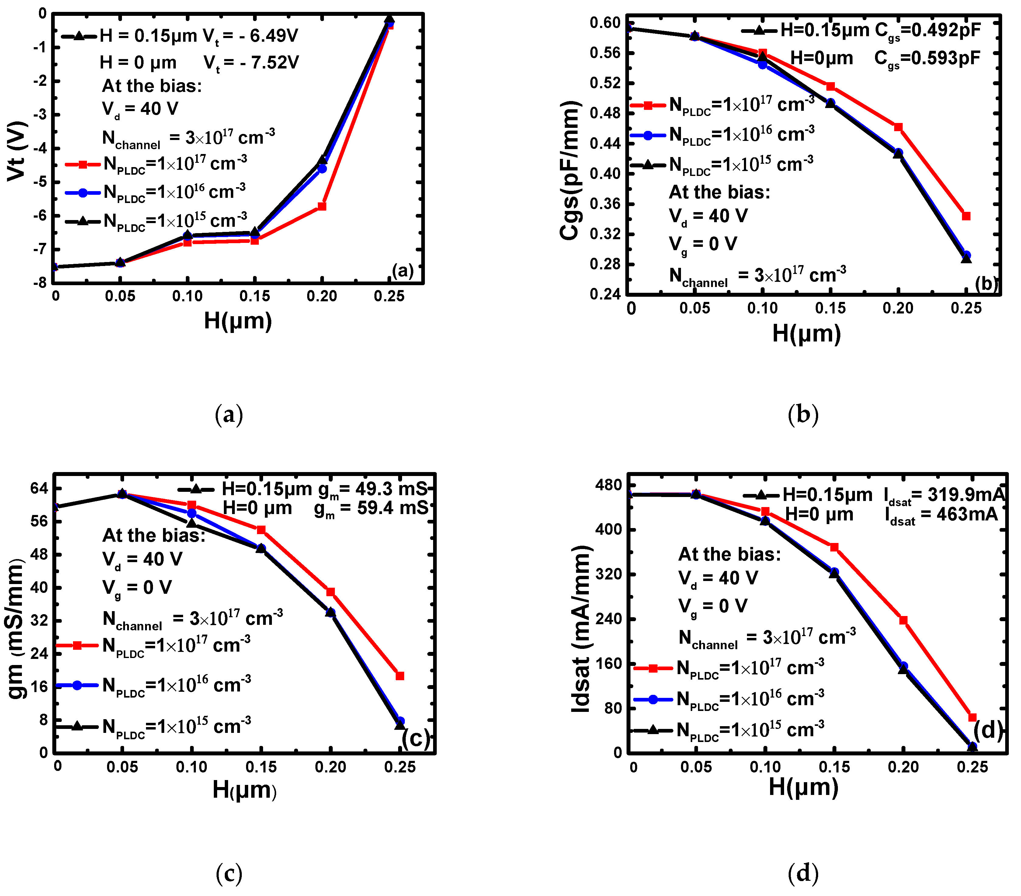
As showing in Figure 2, the parameters of the device are greatly affected by the doping concentration (NPLDC) and thickness (H) of the PLDC. The effect of NPLDC and H on Vt is shown in Figure 2a. With the decrease of NPLDC, the absolute value of Vt decreases obviously. When H increases, the Vt overall trend is also decreasing. This is because the changes in NPLDC and H directly control the total carrier concentration in the channel, and Vt is proportional to the total carrier. Figure 2b shows the effects of NPLDC and H on Cgs. With the decrease of NPLDC and the increase of H, Cgs decreases. On the one hand, the PLDC suppresses the under-gate depletion layer extending to the source side, and on the other hand, it reduces the total number of carriers in the channel, thereby reducing the input capacitance of the device. In the Figure 2c, gm increases first and then decreases. The reason for this formation may be that the thinner low doped layer can increase the gate’s ability to control the current by inhibiting the diffusion of the depletion layer to some extent. When H is thick enough, the ability of the gate to control the current will be reduced. So, gm decreases. In Figure 2d, Idsat is roughly decreased as H increases and NPLDC decreases. This is mainly caused by the decrease of the channel carrier concentration. When H is 0.25 μm, the parameters exhibit a sharp decrease and the DC characteristic of the device becomes poor. It is indicated by the simulation results that the PLDC-MESFET has smaller values of Cgs, gm, Vt and Idsat as compared to those of the original device.
3.2. The Influences of Doping Concentration and Thickness on the PAE
The influences of the doping concentration and thickness on the PAE are shown in Figure 3. It can be seen that when H is smaller than 0.20 μm, the PAE of the device increases with the decrease of NPLDC. When H is 0.20 μm and NPLDC is 1 × 1015 cm−3 or 1 × 1016 cm−3, the PAE of the device decreases sharply. When H is 0.20 μm and NPLDC is 1 × 1017 cm−3, the PAE of the device increases. When H is 0.25 μm, the simulation results show that the DC characteristics and AC characteristics of the device are poor, and the PAE of these structures is low. The maximum value of the PAE is obtained when the NPLDC is 1 × 1015 cm−3, the H is 0.15 μm. The PAE of the new device is 43.67% while the PAE of the original device is 23.43%. The optimized PAE is increased by 86.38%. The PAE of the IUU-MESFET and DRBL AlGaN/GaN HEMT increase 18% and 48%, respectively. So, the PLDC has a great effect on improving the PAE of the device. In the paper 107 W CW SiC MESFET with 48.1% PAE, the experimental PAE of the device at 2 W (33 dBm) is close to 25% [17]. The PAE of the DR-MESFET is 23.43% at 0.63 W (28 dBm). This is essentially consistent with the simulation results.
3.3. Mechanism Discussion
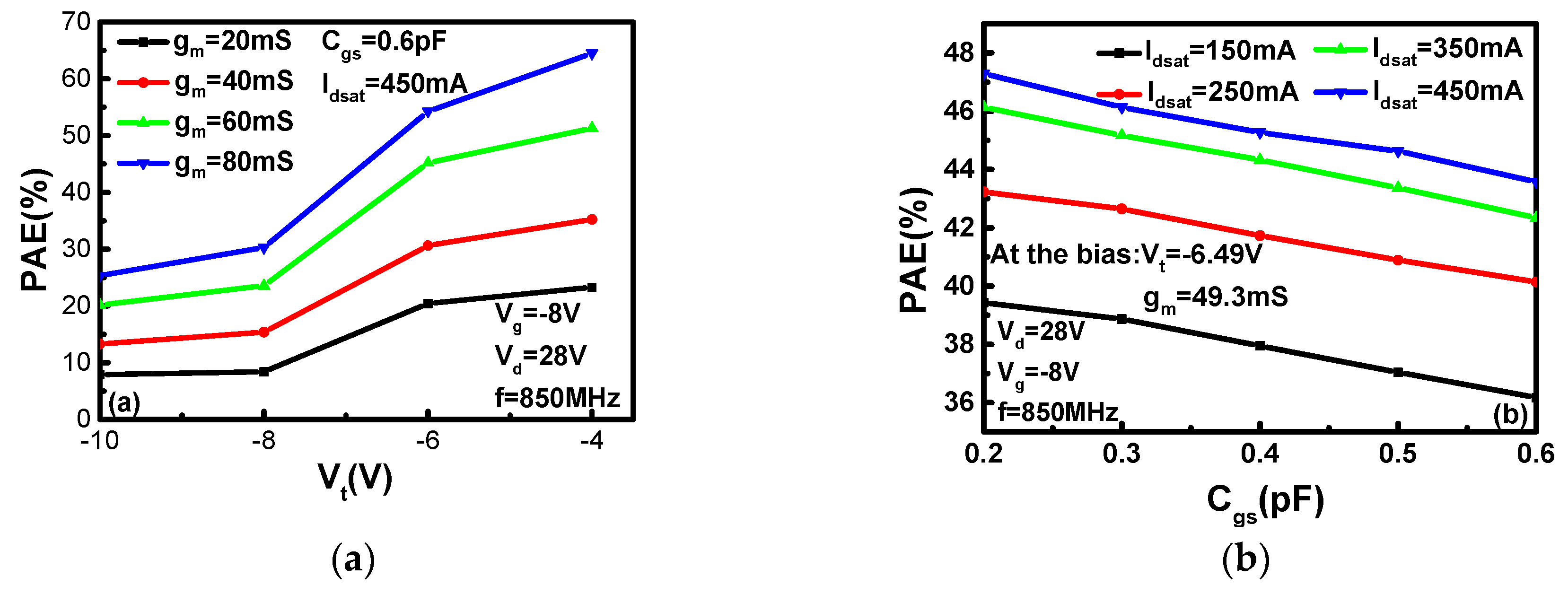
Figure 4a,b shows the influence of the parameters on PAE at the same bias when Vgs is −8.0 V, Vds is 28 V, RF is 850 MHz and Pavs_dBm is 28 dBm. As shown in Figure 4a, the PAE increases with the increase of Vt when gm is a constant. When Vt is a constant, the PAE also increases with the increase of gm. When gm is between 40 and 60 mS, the PAE of the device has the biggest change. This can be observed by the distance between the two curves. Figure 4b shows the influence of Idsat and Cgs on the PAE. With the increase of Cgs, the PAE decreases. With the increase of Idsat, the PAE increase. Furthermore, the larger Idsat is, the slower PAE increases.
From the analysis above, it can be concluded that the smaller the absolute value of Vt, the bigger the PAE, and the smaller the Cgs, the bigger the PAE. For gm, a bigger gm means a higher current gain, so it a larger output can be obtained under the same input. According to Figure 4a, the PAE is proportional to gm. This is the reason why the PAE of the device decreases sharply when H is 0.20 μm and NPLDC is 1 × 1015 cm−3 or 1 × 1016 cm−3. When H is 0.20 μm and NPLDC is 1 × 1017 cm−3, the PAE of the device increases because gm is not the key factor compared with Vt, Idsat and Cgs. The PAE of the device is decided by the influences of those parameters.
It can be seen that the doping concentration and thickness of the PLDC are optimized to be NPLDC = 1 × 1015 cm−3 and H = 0.15 μm. Table 1 shows some main parameters of the two devices. It can be seen that the PAE of the PLDC-MESFET is 43.67%, which is higher than the PAE of 23.43% of the DR-MESFET. Compared the two devices, the PLDC-MESFET has a smaller threshold voltage, smaller input capacitance, smaller transconductance and smaller saturation current than the DR-MESFET. The increase of the PAE is influenced by the combination of these parameters. When the absolute value of Vt decreases, the device is easier to turn on and gains a larger output current. So, the output power Pout increases and a higher PAE is reached. According to Formula (2) [16], a smaller input capacitance Cgs means the device has less energy loss when working in RF (charging and discharging).
where Pdyn is the dynamic power consumption flipped once, EVD is the energy obtained from the power source, Ec is the capacitor stored energy, C is the gate–source capacitor and VD is the drain voltage. A small Cgs also increases the input impedance of the device. Therefore, Pout of the device increases and Pin decreases. For Idsat, a small Idsat indicates a small Pout. Under the influence of these parameters, the device has a big PAE. In there, gm is sacrificed to obtain a higher PAE. Though a larger gm is helpful to increase PAE, the influences of the other parameters on PAE are more obvious. So, the maximum value of PAE is 43.67% when NPLDC is 1 × 1015 cm−3 and H is 0.15 μm, as obtained by sacrificing some of the DC performances of the device.
4. Conclusions
An improved 4H-SiC MESFET with a partially low doped channel is designed and simulated in this paper to increase the PAE of the device. The results show that the maximum PAE of the PLDC-MESFET is 43.67%, while the PAE of the DR-MESFET is 23.43%; the optimized PAE was increased by 86.38%. A way to design an energy efficient amplifier is proposed in this paper by balancing the parameters of the device. This ensures that the device has lower energy consumption at the same output power, which has great significance for RF power amplifier applications.
Author Contributions
Project administration, H.J.; writing—original draft preparation, Y.T.; writing—review and editing, T.L., S.Z., Y.L., Y.Y.; Data curation, X.W.; Formal analysis, T.Z.
Funding
This work was supported by the National Natural Science Foundation of China (NSFC) under Grant No. 61671343.
Conflicts of Interest
The authors declare no conflict of interest.
References
- Riaz, M.; Ahmed, M.M.; Munir, U. An improved model for current voltage characteristics of submicron SiC MESFETs. Solid State Electron. 2016, 121, 54–61. [Google Scholar] [CrossRef]
- Nakashima, S.; Harima, H. Raman Investigation of SiC Polytypes. Phys. Status Solidi Appl. Res. 2015, 162, 39–64. [Google Scholar] [CrossRef]
- Kirschman, R. Status of Silicon Carbide (SiC) as a WideBandgap Semiconductor for HighTemperature Applications: A Review. Solid-State Electron. 1996, 39, 1409–1422. [Google Scholar]
- Holmes, J.; Dutta, M.; Koeck, F.A.; Brown, J.; Fox, B.; Hathwar, R.; Johnson, H.; Malakoutian, M.; Saremi, M.; Zaniewski, A.; et al. A 4.5-μm PIN diamond diode for detecting slow neutrons. Nucl. Instrum. Methods Phys. Res. A 2018, 903, 297–301. [Google Scholar] [CrossRef]
- Saremi, M.; Hathwar, R.; Dutta, M. Analysis of the reverse I-V characteristics of diamond-based PIN diodes. Appl. Phys. Lett. 2017, 111, 043507. [Google Scholar] [CrossRef]
- Aminbeidokhti, A.; Dimitrijev, S.; Kumar Hanumanthappa, A. Gate-Voltage Independence of Electron Mobility in Power AlGaN/GaN HEMTs. IEEE Trans. Electron Devices 2016, 63, 1013–1019. [Google Scholar] [CrossRef]
- Aminbeidokhti, A.; Dimitrijev, S.; Han, J. The Power Law of Phonon-Limited Electron Mobility in the 2-D Electron Gas of AlGaN/GaN Heterostructure. IEEE Trans. Electron Devices 2016, 63, 2214–2218. [Google Scholar] [CrossRef]
- Yakimova, R.; Syväjarvi, M.; Iakimov, T.; Jacobsson, H.; Kakanakova-Georgieva, A.; Råback, P.; Janzén, E. Growth of silicon carbide: Process-related defects. Appl. Surf. Sci. 2001, 184, 27–36. [Google Scholar] [CrossRef]
- Jia, H.J.; Yang, Z.H.; Ma, P.M. A novel 4H-SiC MESFET with localized high-doped P-buffer layer. In Proceedings of the IEEE International Conference on Solid-State and Integrated Circuit Technology, Hangzhou, China, 25–28 October 2016; pp. 1086–1088. [Google Scholar]
- Jia, H.J.; Zhu, S.W.; Hu, M. An improved DRBL AlGaN/GaN HEMT with high power added efficiency. Mater. Sci. Semicond. Process. 2019, 89, 212–215. [Google Scholar] [CrossRef]
- Jia, H.J.; Hu, M.; Zhu, S.W. An Improved UU-MESFET with High Power Added Efficiency. Micromachines 2018, 9, 573. [Google Scholar] [CrossRef] [PubMed]
- Zhu, C.L.; Tin, C.C.; Zhang, G.H.; Yoon, S.F.; Ahn, J. Improved performance of SiC MESFETs using double-recessed structure. Microelectron. Eng. 2005, 83, 92–95. [Google Scholar] [CrossRef]
- Horiuchi, T.; Homma, T.; Murao, Y.; Okumura, K. An asymmetric sidewall process for high performance LDD MOSFET. IEEE Trans. Electron Devices 1994, 41, 186–190. [Google Scholar] [CrossRef]
- Synopsys Inc. Dessis User Guide, User Manuals, Version ISE TCAD 10.0; Synopsys Inc.: Mountain View, CA, USA, 2004. [Google Scholar]
- Angilent Technologies. ADS Documentation, User Manuals, Version ADS2015; Angilent Technologies: Santa Clara, CA, USA, 2015. [Google Scholar]
- Lee, T.H. The Design of CMOS Radio-Frequency Integrated Circuits; Cambridge University Press: Cambridge, UK, 1998. [Google Scholar]
- Tao, Y.; Bai, S. 107W CW SiC MESFET with 48.1% PAE. In Proceedings of the IEEE International Symposium on Microwave, Antenna, Propagation and EMC Technologies for Wireless Communications, Chengdu, China, 29–31 October 2013. [Google Scholar]
Figure 1.
Schematic cross-sections of the (a) DR 4H-SiC MESFET, (b) partially low doped channel (PLDC) 4H-SiC MESFET.
Figure 1.
Schematic cross-sections of the (a) DR 4H-SiC MESFET, (b) partially low doped channel (PLDC) 4H-SiC MESFET.

Figure 2.
The effect of NPLDC and H on the device parameters: (a) Vt-NPLDC and H, (b) Cgs-NPLDC and H, (c) gm-NPLDC and H, (d) Idsat-NPLDC and H.
Figure 2.
The effect of NPLDC and H on the device parameters: (a) Vt-NPLDC and H, (b) Cgs-NPLDC and H, (c) gm-NPLDC and H, (d) Idsat-NPLDC and H.

Figure 3.
The effects of NPLDC and H on the PAE.

Figure 4.
The effect of device parameters on PAE: (a) PAE-Vt and gm, (b) PAE-Cgs and Idsat.


Table 1.
Comparison of performance parameters of the two structures.
| Parameters | DR 4H-SiC MESFET | PLDC 4H-SiC MESFET |
|---|---|---|
| Idsat (mA/mm) | 448.00 | 319.90 |
| Vb (V) | 125.35 | 130.20 |
| gm (mS/mm) | 59.30 | 49.30 |
| Vt (V) | −7.52 | −6.49 |
| Cgs (pF/mm) | 0.59 | 0.49 |
| PAE (%) | 23.43 | 43.67 |
© 2019 by the authors. Licensee MDPI, Basel, Switzerland. This article is an open access article distributed under the terms and conditions of the Creative Commons Attribution (CC BY) license (http://creativecommons.org/licenses/by/4.0/).
Share and Cite
MDPI and ACS Style
Jia, H.; Tong, Y.; Li, T.; Zhu, S.; Liang, Y.; Wang, X.; Zeng, T.; Yang, Y. An Improved 4H-SiC MESFET with a Partially Low Doped Channel. Micromachines 2019, 10, 555. https://doi.org/10.3390/mi10090555
AMA Style
Jia H, Tong Y, Li T, Zhu S, Liang Y, Wang X, Zeng T, Yang Y. An Improved 4H-SiC MESFET with a Partially Low Doped Channel. Micromachines. 2019; 10(9):555. https://doi.org/10.3390/mi10090555
Chicago/Turabian StyleJia, Hujun, Yibo Tong, Tao Li, Shunwei Zhu, Yuan Liang, Xingyu Wang, Tonghui Zeng, and Yintang Yang. 2019. "An Improved 4H-SiC MESFET with a Partially Low Doped Channel" Micromachines 10, no. 9: 555. https://doi.org/10.3390/mi10090555
Note that from the first issue of 2016, this journal uses article numbers instead of page numbers. See further details here.