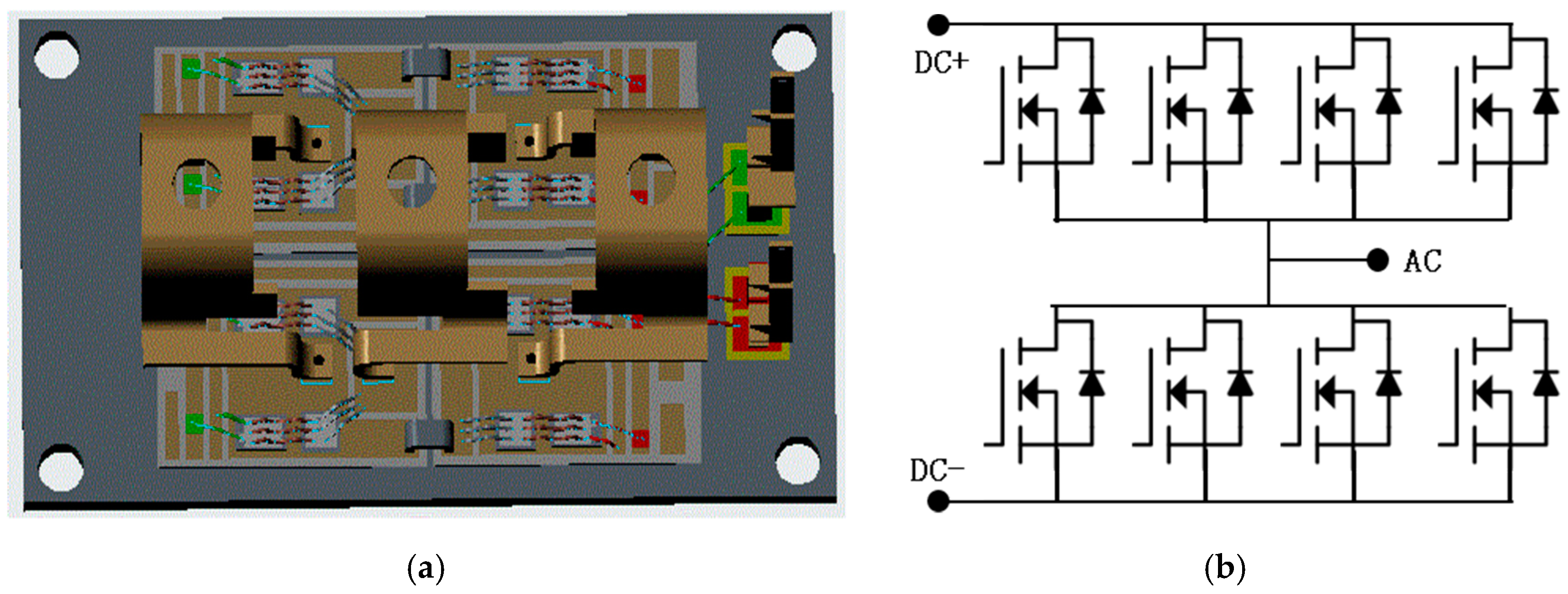
4.1. Equivalent Model of Gate-Source Path of SiC Power Module
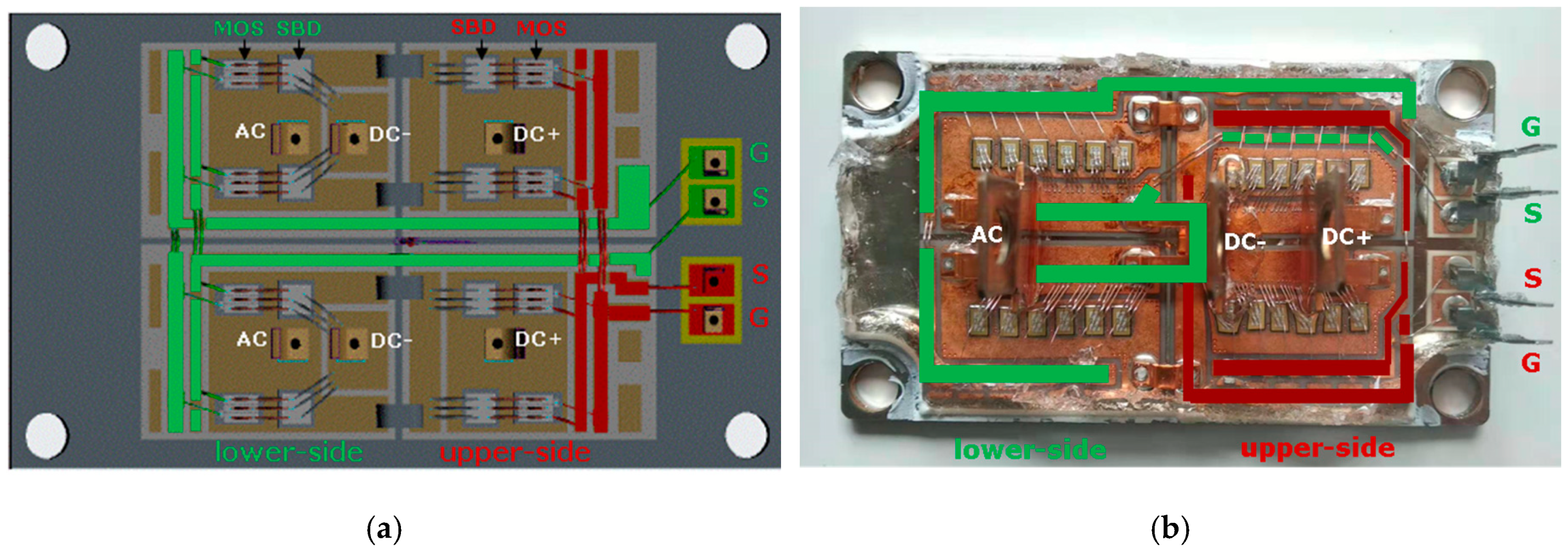
The equivalent circuit model of the gate loop is obtained based on the analysis of the actual physical structure of the power module and the output stage of the gate driver circuit. For the standard package outline of the half-bridge module, the internal structure of the upper-side is different from that of the lower-side. The routings of drain circuit and gate circuit inside the power module are shown in
Figure 10a,b, respectively. Since all the gate input terminals are placed to the outer edge area of the upper-side of the power module, the gate routings of the lower-side must pass through the upper-side before connecting to the power chips of the lower-side.
Compared with gate-source path of the upper-side, the gate-source path of the lower-side is much longer, the input signal must pass through the whole power module before connecting to the power chips (see
Figure 2a,
Figure 10). As a result, the location of the lumped parasitic inductance of the gate loop in upper-side is different from that of lower-side in our equivalent circuit models at turn-on transient. That is to say, the topology of the equivalent circuit model of the gate driver loop is different between upper-side and lower-side for the developed half-bridge module.
In the previous analysis of the experimental results, we found that the output power of power module affects the characteristics of . As the common source inductance is minimized in our design, the effect of common source inductance on turn-on transient can be ignored. We put emphasis on the coupling effect of drain circuit to gate driver loop, and it will be discussed in the following.
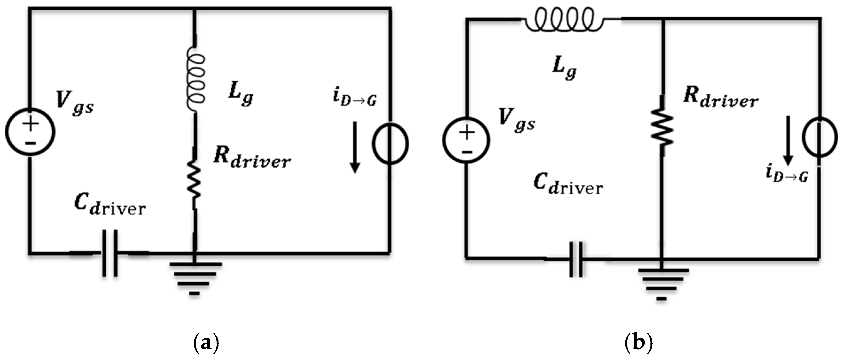
Based on the internal structure of the power module in
Figure 10, the equivalent RLC circuit models of the gate driver loop in turn-on transient for the upper-side and lower-side are established and shown in
Figure 11a, b, respectively. The coupling effect is equivalent to a short-time current source. As this short-time current source is an external factor for the gate driver loop, it is parallel-connected to the equivalent circuit in the model. With the help of the models,
characteristics at the turn-on transient can be simulated.
In
Figure 11,
stands for the total stray inductance of gate driver loop, it includes the gate-source routings inside module,
, and the stray inductance of output paths of gate driver circuit,
, which can be expressed by Equation (1),
The
is the resistance of the whole gate driver loop, it includes the stray resistance of gate-source routings,
, the external gate resistance
and internal resistance of SiC-MOSFET,
, and the output resistance of gate driver circuit,
, which can be expressed by Equation (2),
The
is the parasitic capacitance of the total routings of the gate driver loop. The parasitic parameters can be extracted by Q3D software and they are listed in
Table 6.
The value of the equivalent current source stands for the extent of this influence, which is designated as
. The higher the slew rate of
, the higher the
. The
is given by Equation (3),
The value of is determined by and . The capacitance of power chips increases sharply as the voltage decreases at the turn-on transient, and the value of is also increased. Therefore, the coupling effect between the drain loop and gate driver loop is enhanced significantly due to the sharply rising at turn-on transient.
If the increase in output power is equivalent to a rise of
,
is getting higher at an increased output power. Thus, the current
can reflect the extent of influence of output power on gate driver loop in our equivalent circuit model. The equivalent current
at the turn-on transient for the experiment can be calculated by Equation (3) and they are summarized in
Table 5.
Based on the RLC circuit model, the extracted parameters of the power module and gate driver circuit, as well as the calculated
from the experimental results, the generation mechanism of the characteristics of
voltage spike for full-SiC power module at turn-on transient can be studied quantitatively by LTspice software. The respective values of
for case_1, case_2, and case_3 in simulation are the same with those in experiment (
Table 5), while the values of the parasitic parameters used in simulation are from
Table 6.
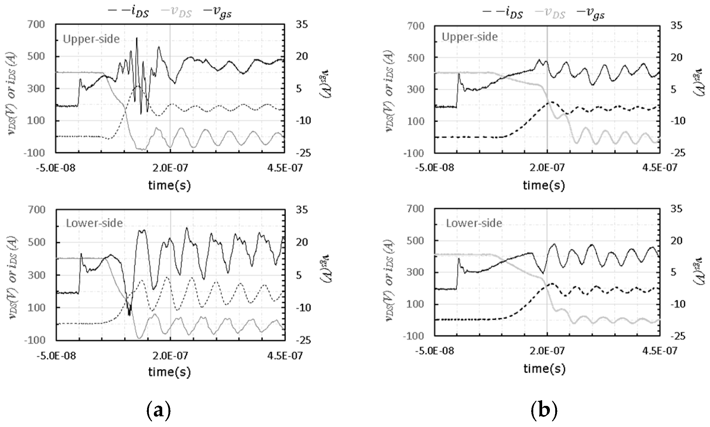
For the upper-side,
is set to 15 V, the current source
starts to output pulse at time of 5 ns and it lasts a time interval of 7 ns in the simulation, the value of
is as listed in
Table 5. The simulation results for the three cases as studied by the experiments in
Section 3 are shown in
Figure 12.
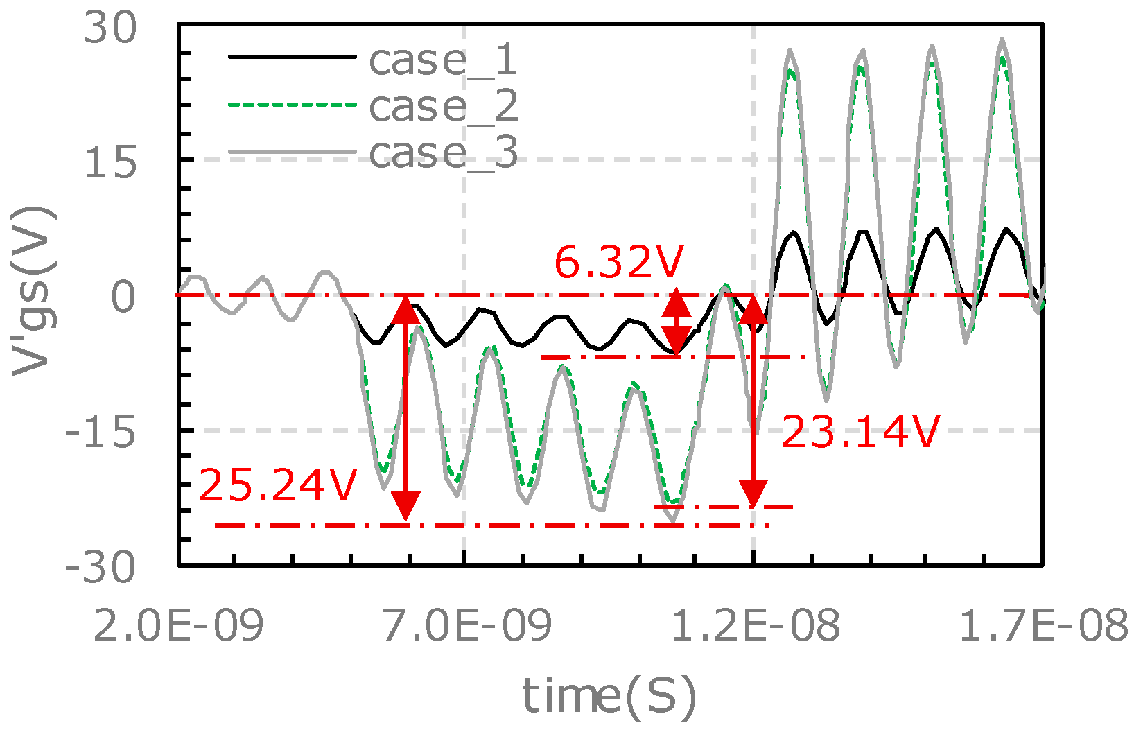
As the output power increases, the rises from 0.47 A to 1.85 A accordingly, the gate-source voltage minus the DC voltage bias () is pulled down to a lower value. At the meantime, the gate source voltage is accompanied with a high frequency oscillation. The oscillation frequency is 83.3 MHz, which is the same as that of the experimental results. The oscillation frequency doesn’t vary with the values as it is only related to the parasitic parameters of both the gate driver circuit and gate-source routings inside the power module. When the equivalent current source starts to output pulse the tumbles, and the rebounds immediately when the current source output is terminated.
For the lower-side, the
is set to 15 V, the equivalent current source of
starts to output pulse at time of 6 ns and it lasts a time interval of 5 ns in the simulation. The simulation results for the three cases as studied by the experiments in
Section 3 are shown in
Figure 13. As the output power increases, the
rises from 0.35 A to 1.34 A accordingly,
is pulled down to a lower value. There is no high frequency oscillation observed.
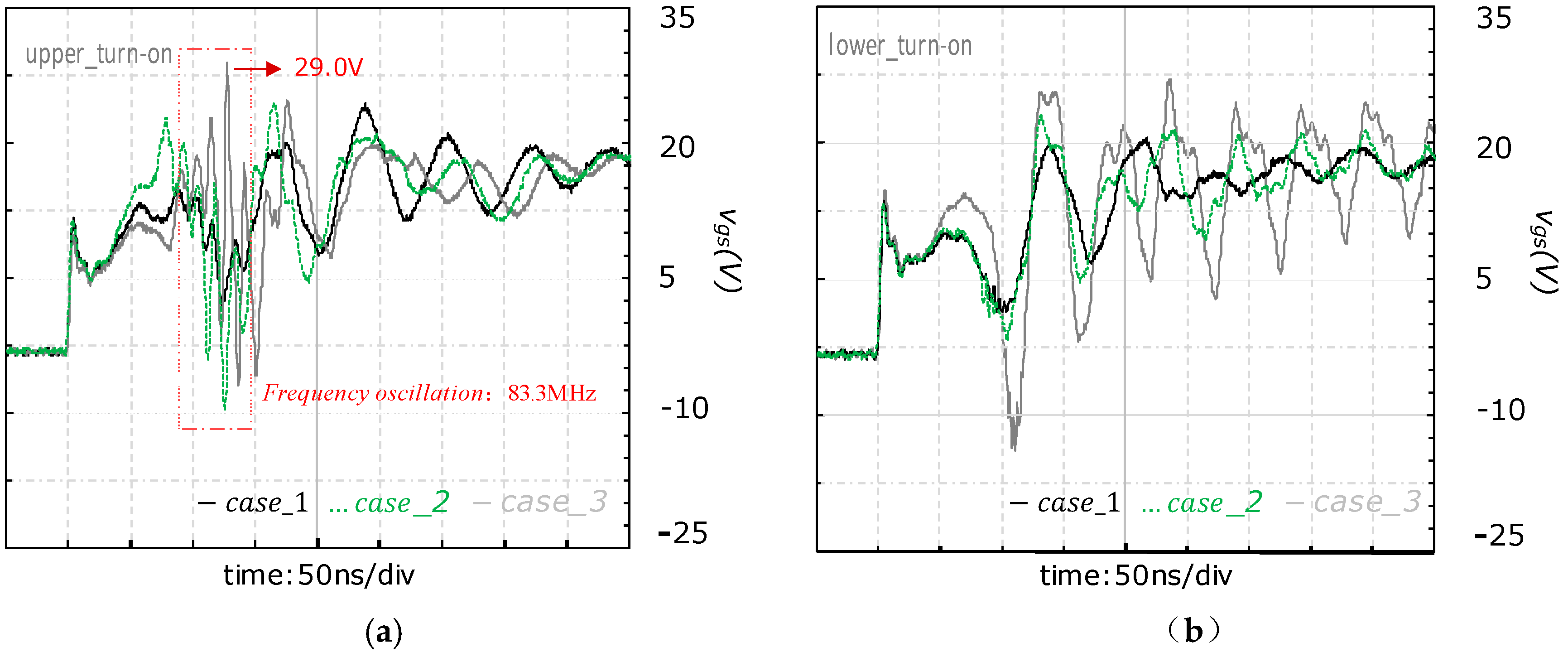
The characteristics of
pulling down in simulation are compared with the experimental results (as shown in
Figure 9). The amplitude of
pulling-down and oscillation for the upper-side and lower-side in different cases are listed in
Table 7. For the characteristics of high frequency oscillation, the simulation is in good agreement with the experimental results. For the characteristics of the pulling down amplitude of
spike, the simulation is almost in agreement with the experimental results except the upper-side.
The pulling down amplitude of
spike of the lower-side increases as the output power rises in both simulation and experiment, but the pulling down amplitude of
of the upper-side in simulation is different from the experiment. In simulation, the pulling down amplitude of
rises as output increases, but in experimental results the largest pulling down amplitude of
occurred in case_2 rather than case_3. This abnormal phenomenon in the experiment is mainly attributed to the high frequency oscillation on the pulling down waveform of
. As shown in
Figure 9a, there is an excessively positive voltage spike of 29.0 V in case_3 during the high frequency oscillation process, while the high frequency oscillation doesn’t bring the voltage spike back to a lower point as that in case_2.
Overall, the characteristics of spike in simulation almost coincide with that of the experiment results. This proves the rationality of our modeling and analysis about the generation mechanism of voltage spike characteristics for SiC power module.
As depicted previously, the negative voltage spike is correlated to the slew rate of and the resistance of the gate driver loop. On one hand, the increased gate resistance can reduce , and decrease the coupling between the drain loop and gate driver loop due to a lower at a slower slew rate of . On the other hand, the larger the gate resistance of the gate driver loop, the smaller the gate current and voltage spike, and less serious the oscillation at turn-on switching transient. Although the coupling effects are different between the upper-side and lower-side, both the negative spike and high frequency oscillation could shrink as the resistance of the gate driver circuit rises. Another experiment and simulation with a higher external gate resistance are carried out to further verify our RLC circuit model and analysis.
4.2. Verification for the Proposed RLC Circuit Model and Analysis
A resistor of 5 Ω instead of the previous external gate resistor of 2.4 Ω is used in the new experiment. The case_3 is selected for the case study as the output power is highest and the negative spike/oscillation is the most significant in this case. The experimental results are shown in
Figure 14.
There is neither voltage pulling down nor high frequency oscillation observed for the upper-side (
Figure 14a), but a pulling down effect and a spike of
is observed for the lower-side (
Figure 14b). When the external gate resistance is increased from 2.4 Ω to 5 Ω, the negative spike of
in lower-side is decreased from −13.7 V (in
Figure 8 and
Table 4) to −2.5 V (
Figure 14b). Accordingly, the amplitude of
pulling down is reduced from 28.66 V (in
Figure 8 and
Table 4) to 10.28 V (
Figure 14b).
The experimental results show that the relatively larger external gate resistor can damp the high frequency oscillation in the upper-side and weaken the amplitude of pulling down of at turn-on transient in SiC power module.
The slew rate of
at the turn-on transient are extracted from the experiments and listed in
Table 8. The introduced extra current of
is calculated with Equation (3) and listed in
Table 8 as well.
Compared with that of 2.4 Ω, the slew rate of in the condition of gate resistor of 5 Ω reduces significantly; accordingly, the equivalent current from drain loop to gate driver loop due to the coupling effect at the turn-on transient also decreases dramatically.
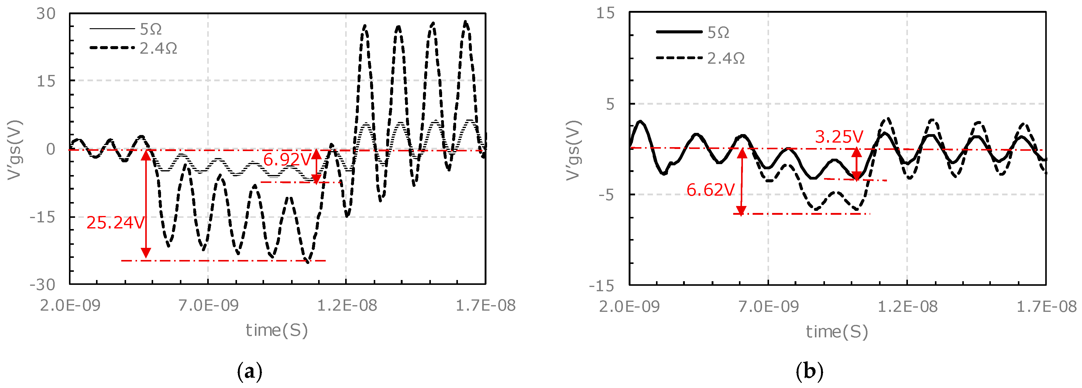
With the proposed equivalent RLC circuit models shown in
Figure 11 and Equations (1)–(3), simulation study with an external gate resistor of 5 Ω is carried out. In this simulation all the parameters are the same as that of the previous simulation except the gate resistance. The simulation results under different external gate resistance conditions are compared in
Figure 15. For the upper-side, the high frequency oscillation is alleviated by the higher gate resistance (5 Ω vs. 2.4 Ω), and the amplitude of
tumbling is reduced from 25.24 V to 6.92 V (72.5% lower). For the lower-side, the amplitude of
tumbling is reduced by ~50% from 6.62 V to 3.25 V.
The characteristics from simulation results (in
Figure 15) are extracted and compared with those from the experimental results in
Figure 8, 14. The compared characteristics contains the amplitude of
pulling down and oscillation. The comparison results are listed in
Table 9.
As the gate resistance rises, the characteristics of high frequency oscillation in the upper-side disappears for both experiment and simulation, the amplitude of the pulling down of in the upper-side is lowered significantly for both experiment and simulation. The pulling down amplitude in the experiment reduces from 28.20 V to zero while it decreases from 25.24 V to 6.92 V in the simulation. The amplitude of the pulling down of in the lower-side is also reduced significantly for both experiment and simulation, which reduces from 28.66 V to 10.28 V in the experiment and decreases from 6.62 V to 3.25 V in the simulation.
The specific amplitudes of the pulling down of
between the simulation and experiment are different, the error could come from the read of d
and the parameter extraction by Q3D software. As shown in
Table 9, the trend of changes in the amplitude of
pulling down and oscillation along with the increase of output power in simulation generally agrees with those of the experimental results. This further confirms the validity of the proposed equivalent RLC circuit model and the rationality of the analysis about the mechanisms behind the
characteristics at turn-on transient for the SiC half-bridge power module.
As guided by the proposed model, the gate driver design must be considered together with the power module design for obtaining an optimized switching performance for the high-power high-frequency SiC power module. For a fabricated power module, we can set the parameters in the model related to the gate driver circuit, such as the in Equation (1), the and in Equation (2). Then the characteristic can be simulated and optimized by tuning the parameters. Thus, a proper design of the gate driver circuit matched with the power module design and output power level can be obtained in a short design cycle.


