A Comparison between Nanogratings-Based and Stress-Engineered Waveplates Written by Femtosecond Laser in Silica


 , and
, and 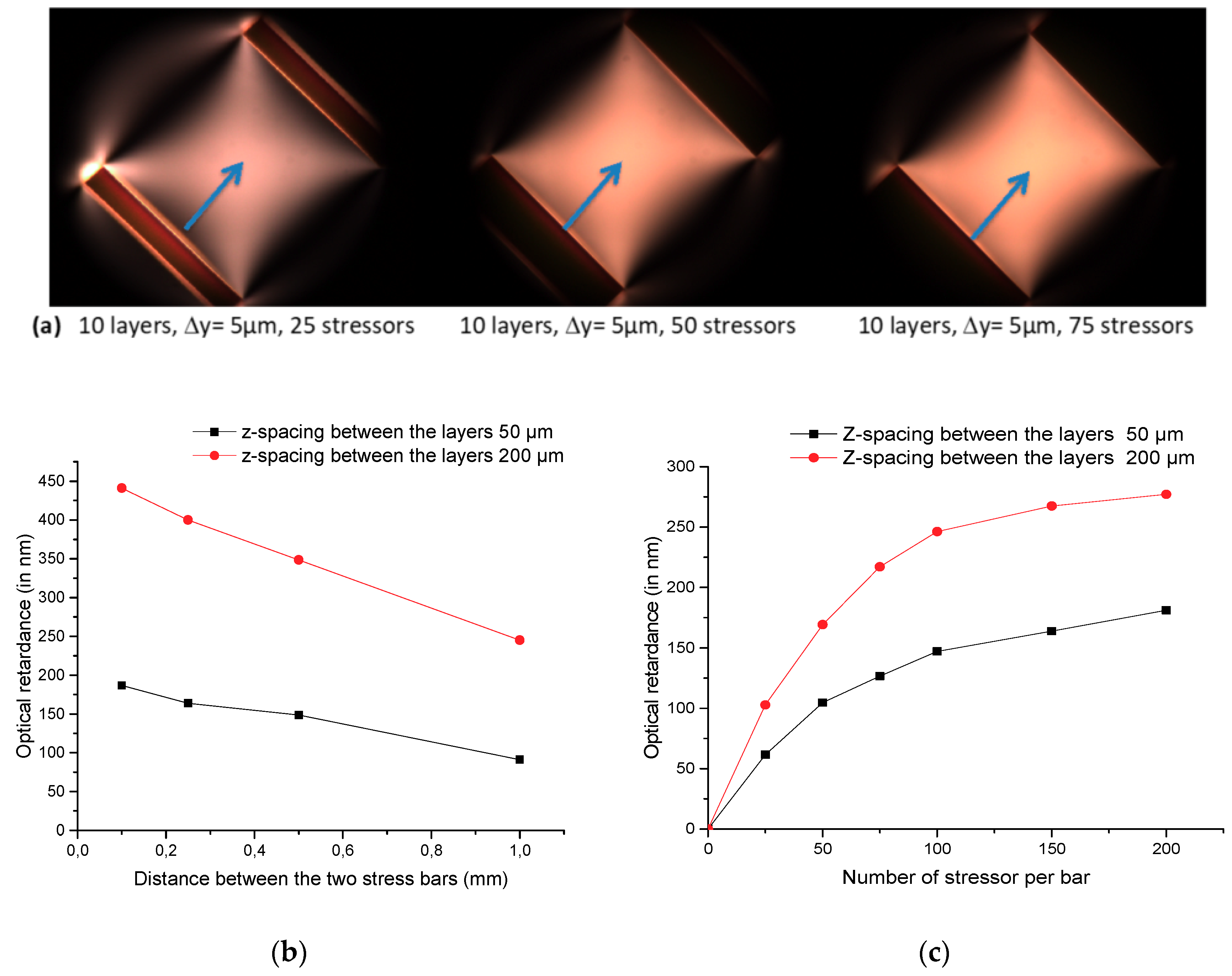
Abstract
:1. Introduction
2. Materials and Methods
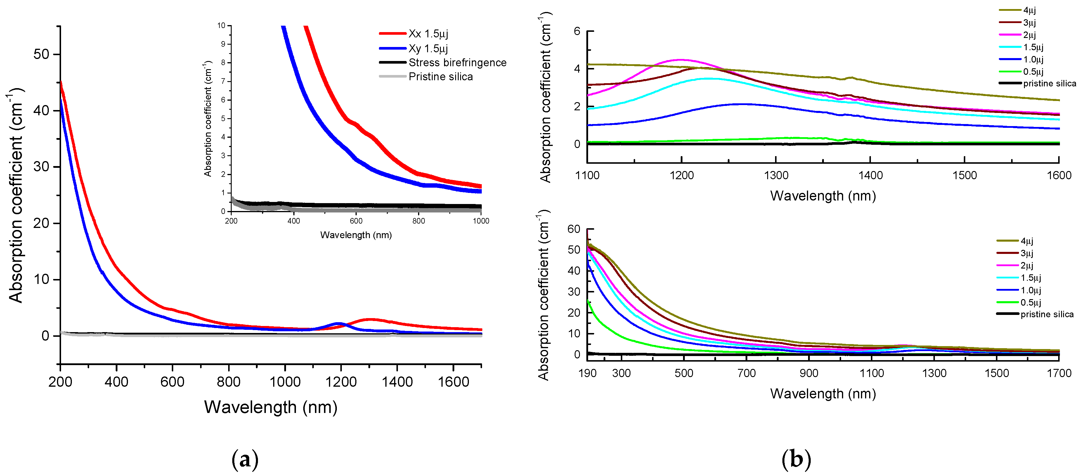
3. Results
4. Conclusions
Author Contributions
Funding
Conflicts of Interest
References
- Shimotsuma, Y.; Kazansky, P.; Qiu, J.; Hirao, K. Self-organized nanogratings in glass irradiated by ultrashort light pulses. Phys. Rev. Lett. 2003, 91. [Google Scholar] [CrossRef] [PubMed] [Green Version]
- Kazansky, P.G.; Inouye, H.; Mitsuyu, T.; Miura, K.; Qiu, J.; Hirao, K.; Starrost, F. Anomalous anisotropic light scattering in Ge-doped silica glass. Phys. Rev. Lett. 1999, 82, 2199–2202. [Google Scholar] [CrossRef]
- Bricchi, E.; Mills, J.; Kazansky, P.; Klappauf, B.; Baumberg, J. Birefringent Fresnel zone plates in silica fabricated by femtosecond laser machining. Opt. Lett. 2002, 27, 2200–2202. [Google Scholar] [CrossRef] [PubMed] [Green Version]
- Sudrie, L.; Franco, M.; Prade, B.; Mysyrowicz, A. Writing of permanent birefringent microlayers in bulk fused silica with femtosecond laser pulses. Opt. Commun. 1999, 171, 279–284. [Google Scholar] [CrossRef]
- Hnatovsky, C.; Taylor, R.; Simova, E.; Bhardwaj, V.; Rayner, D.; Corkum, P. Polarization-selective etching in femtosecond laser-assisted microfluidic channel fabrication in fused silica. Opt. Lett. 2005, 30, 1867–1869. [Google Scholar] [CrossRef] [PubMed]
- Bricchi, E.; Kazansky, P.G. Extraordinary stability of anisotropic femtosecond direct-written structures embedded in silica glass. Appl. Phys. Lett. 2006, 88, 2–4. [Google Scholar] [CrossRef] [Green Version]
- Bricchi, E.; Klappauf, B.G.; Kazansky, P.G. Form birefringence and negative index change created by femtosecond direct writing in transparent materials. Opt. Lett. 2004, 29, 119–121. [Google Scholar] [CrossRef]
- Beresna, M. Polarization Engineering with Ultrafast Laser Writing in Transparent Media. Ph.D. Thesis, University of Southampton, Southampton, UK, 2012. [Google Scholar]
- Beresna, M.; Gecevičius, M.; Kazansky, P.G. Ultrafast laser direct writing and nanostructuring in transparent materials. Adv. Opt. Photonics 2014, 6, 293–339. [Google Scholar] [CrossRef]
- Beresna, M.; Gecevičius, M.; Kazansky, P.G. Harnessing Ultrafast Laser Induced Nanostructures in Transparent Materials. In Progress in Nonlinear Nano-Optics; Springer: Berlin/Heidelberg, Germany, 2015; pp. 31–46. [Google Scholar]
- Drevinskas, R.; Beresna, M.; Zhang, J.; Kazanskii, A.G.; Kazansky, P.G. Ultrafast laser-induced metasurfaces for geometric phase manipulation. Adv. Opt. Mater. 2017, 5. [Google Scholar] [CrossRef]
- Zhang, J.; Geceviçius, M.; Beresna, M.; Kazansky, P.G. 5D Data Storage by Ultrafast Laser Nanostructuring in Glass. In Proceedings of the CLEO: Science and Innovations, San Jose, CA, USA, 9–14 June 2013. CTh5D. 9. [Google Scholar]
- Zhang, J.; Gecevičius, M.; Beresna, M.; Kazansky, P.G. Seemingly unlimited lifetime data storage in nanostructured glass. Phys. Rev. Lett. 2014, 112. [Google Scholar] [CrossRef]
- Ohfuchi, T.; Sakakura, M.; Yamada, Y.; Fukuda, N.; Takiya, T.; Shimotsuma, Y.; Miura, K. Polarization imaging camera with a waveplate array fabricated with a femtosecond laser inside silica glass. Opt. Express 2017, 25, 23738–23754. [Google Scholar] [CrossRef] [PubMed]
- Gecevičius, M.; Beresna, M.; Kazansky, P.G. Polarization sensitive camera by femtosecond laser nanostructuring. Opt. Lett. 2013, 38, 4096–4099. [Google Scholar] [CrossRef] [PubMed]
- Desmarchelier, R.; Lancry, M.; Gecevicius, M.; Beresna, M.; Kazansky, P.; Poumellec, B. Achromatic polarization rotator imprinted by ultrafast laser nanostructuring in glass. Appl. Phys. Lett. 2015, 107, 181111. [Google Scholar] [CrossRef]
- Beresna, M.; Geceviçius, M.; Lancry, M.; Poumellec, B.; Kazansky, P. Broadband anisotropy of femtosecond laser induced nanogratings in fused silica. Appl. Phys. Lett. 2013, 103, 131903. [Google Scholar] [CrossRef]
- Lancry, M.; Poumellec, B.; Canning, J.; Cook, K.; Poulin, J.-C.; Brisset, F. Ultrafast nanoporous silica formation driven by femtosecond laser irradiation. Laser Photonics Rev. 2013, 7, 953–962. [Google Scholar] [CrossRef]
- Tian, J.; Li, R.; Yoo, S.H.; Poumellec, B.; Garcia-Caurel, E.; Ossikovski, R.; Stchakovsky, M.; Eypert, C.; Canning, J.; Lancry, M. Spectral dependence of femtosecond laser induced circular optical properties in silica. Osa Contin. 2019, 2, 1233–1241. [Google Scholar] [CrossRef]
- Bhardwaj, V.; Corkum, P.; Rayner, D.; Hnatovsky, C.; Simova, E.; Taylor, R. Stress in femtosecond-laser-written waveguides in fused silica. Opt. Lett. 2004, 29, 1312–1314. [Google Scholar] [CrossRef]
- Dürr, F.; Limberger, H.; Salathe´, R.; Hindle, F.; Douay, M.; Fertein, E.; Przygodzki, C. Tomographic measurement of femtosecond-laser induced stress changes in optical fibers. Appl. Phys. Lett. 2004, 84, 4983–4985. [Google Scholar] [CrossRef] [Green Version]
- Poumellec, B.; Sudrie, L.; Franco, M.; Prade, B.; Mysyrowicz, A. Femtosecond laser irradiation stress induced in pure silica. Opt. Express 2003, 11, 1070–1079. [Google Scholar] [CrossRef]
- Champion, A.; Bellouard, Y. Direct volume variation measurements in fused silica specimens exposed to femtosecond laser. Opt. Mater. Express 2012, 2, 789–798. [Google Scholar] [CrossRef] [Green Version]
- Bellouard, Y.; Champion, A.; McMillen, B.; Mukherjee, S.; Thomson, R.R.; Pépin, C.; Gillet, P.; Cheng, Y. Stress-state manipulation in fused silica via femtosecond laser irradiation. Optica 2016, 3, 1285–1293. [Google Scholar] [CrossRef]
- Canning, J.; Lancry, M.; Cook, K.; Weickman, A.; Brisset, F.; Poumellec, B. Anatomy of a femtosecond laser processed silica waveguide [Invited]. Opt. Mater. Express 2011, 1, 998–1008. [Google Scholar] [CrossRef]
- Champion, A.; Beresna, M.; Kazansky, P.; Bellouard, Y. Stress distribution around femtosecond laser affected zones: Effect of nanogratings orientation. Opt. Express 2013, 21, 24942–24951. [Google Scholar] [CrossRef] [PubMed]
- Yuan, L.; Cheng, B.; Huang, J.; Liu, J.; Wang, H.; Lan, X.; Xiao, H. Stress-induced birefringence and fabrication of in-fiber polarization devices by controlled femtosecond laser irradiations. Opt. Express 2016, 24, 1062–1071. [Google Scholar] [CrossRef]
- Fernandes, L.A.; Grenier, J.R.; Herman, P.R.; Aitchison, J.S.; Marques, P.V. Stress induced birefringence tuning in femtosecond laser fabricated waveguides in fused silica. Opt. Express 2012, 20, 24103–24114. [Google Scholar] [CrossRef]
- Fernandes, L.A.; Grenier, J.R.; Marques, P.V.; Aitchison, J.S.; Herman, P.R. Strong birefringence tuning of optical waveguides with femtosecond laser irradiation of bulk fused silica and single mode fibers. J. Lightwave Technol. 2013, 31, 3563–3569. [Google Scholar] [CrossRef] [Green Version]
- Beckley, A.M.; Brown, T.G.; Alonso, M.A. Full poincaré beams. Opt. Express 2010, 18, 10777–10785. [Google Scholar] [CrossRef]
- Fernandes, L.A.; Grenier, J.R.; Herman, P.R.; Aitchison, J.S.; Marques, P.V. Femtosecond laser writing of waveguide retarders in fused silica for polarization control in optical circuits. Opt. Express 2011, 19, 18294–18301. [Google Scholar] [CrossRef] [Green Version]
- Fernandes, L.A.; Grenier, J.R.; Herman, P.R.; Aitchison, J.S.; Marques, P.V. Femtosecond laser fabrication of birefringent directional couplers as polarization beam splitters in fused silica. Opt. Express 2011, 19, 11992–11999. [Google Scholar] [CrossRef]
- McMillen, B.; Bellouard, Y. Direct-write diffracting tubular optical components using femtosecond lasers. In Proceedings of the Frontiers in Ultrafast Optics: Biomedical, Scientific, and Industrial Applications XIV, San Francisco, CA, USA, 2–5 February 2014; p. 89720Z. [Google Scholar]
- McMillen, B.; Athanasiou, C.; Bellouard, Y. Femtosecond laser direct-write waveplates based on stress-induced birefringence. Opt. Express 2016, 24, 27239–27252. [Google Scholar] [CrossRef]
- Beresna, M.; Brambilla, G.; Juodkazis, S.; Wang, X.; Rumpf, R. Geometric phase via stress induced birefringence. In Proceedings of the CLEO-Pacific Rim, Singapore, 31 July–4 August 2017; p. 2. [Google Scholar]
- Tian, J.; Lancry, M.; Yoo, S.H.; Garcia-Caurel, E.; Ossikovski, R.; Poumellec, B. Study of femtosecond laser-induced circular optical properties in silica by Mueller matrix spectropolarimetry. Opt. Lett. 2017, 42, 4103–4106. [Google Scholar] [CrossRef] [PubMed]
- Tian, J.; Desmarchelier, R.; Poumellec, B.; Lancry, M. Femtosecond laser-induced circular dichroism in silica: Dependence on energy and focusing depth. Nucl. Instrum. Methods Phys. Res. Sect. B Beam Interact. Mater. At. 2018, 435, 258–262. [Google Scholar] [CrossRef]
- Garcia-Caurel, E.; De Martino, A.; Gaston, J.-P.; Yan, L. Application of spectroscopic ellipsometry and Mueller ellipsometry to optical characterization. Appl. Spectrosc. 2013, 67, 1–21. [Google Scholar] [CrossRef] [Green Version]
- Arteaga, O.; Ossikovski, R. Complete Mueller matrix from a partial polarimetry experiment: The 12-element case. JOSA A 2019, 36, 416–427. [Google Scholar] [CrossRef] [PubMed]
- Ossikovski, R.; Arteaga, O. Completing an experimental nondepolarizing Mueller matrix whose column or row is missing. J. Vac. Sci. Technol. B Nanotechnol. Microelectron. Mater. Process. Meas. Phenom. 2019, 37. [Google Scholar] [CrossRef]
- Ossikovski, R. Differential matrix formalism for depolarizing anisotropic media. Opt. Lett. 2011, 36, 2330–2332. [Google Scholar] [CrossRef] [PubMed]
- Ossikovski, R.; Arteaga, O. Statistical meaning of the differential Mueller matrix of depolarizing homogeneous media. Opt. Lett. 2014, 39, 4470–4473. [Google Scholar] [CrossRef]
- McMillen, B.; Bellouard, Y. On the anisotropy of stress-distribution induced in glasses and crystals by non-ablative femtosecond laser exposure. Opt. Express 2015, 23, 86–100. [Google Scholar] [CrossRef] [Green Version]
- Streltsov, A.M.; Borrelli, N.F. Study of femtosecond-laser-written waveguides in glasses. JOSA B 2002, 19, 2496–2504. [Google Scholar] [CrossRef]
- Yeh, P. A new optical model for wire grid polarizers. Opt. Commun. 1978, 26, 289–292. [Google Scholar] [CrossRef]
- Skuja, L.; Hirano, M.; Hosono, H.; Kajihara, K. Defects in oxide glasses. Phys. Status Solidi (C) 2005, 2, 15–24. [Google Scholar] [CrossRef]
- Lancry, M.; Desmarchelier, R.; Cook, K.; Poumellec, B.; Canning, J. Compact Birefringent Waveplates Photo-Induced in Silica by Femtosecond Laser. Micromachines 2014, 5, 825–838. [Google Scholar] [CrossRef] [Green Version]
- Richter, S.; Heinrich, M.; Döring, S.; Tünnermann, A.; Nolte, S.; Peschel, U. Nanogratings in fused silica: Formation, control, and applications. J. Laser Appl. 2012, 24, 042008(042001)–042008(042008). [Google Scholar] [CrossRef]
- Poumellec, B.; Lancry, M. Kinetics of Thermally Activated Physical Processes in Disordered Media. Fibers 2015, 3, 206–252. [Google Scholar] [CrossRef] [Green Version]
- Čerkauskaitė, A. Ultrafast Laser Nanostructuring for Photonics and Information Technology; University Of Southampton: Southampton, UK, 2018. [Google Scholar]


© 2020 by the authors. Licensee MDPI, Basel, Switzerland. This article is an open access article distributed under the terms and conditions of the Creative Commons Attribution (CC BY) license (http://creativecommons.org/licenses/by/4.0/).
Share and Cite
Tian, J.; Yao, H.; Cavillon, M.; Garcia-Caurel, E.; Ossikovski, R.; Stchakovsky, M.; Eypert, C.; Poumellec, B.; Lancry, M. A Comparison between Nanogratings-Based and Stress-Engineered Waveplates Written by Femtosecond Laser in Silica. Micromachines 2020, 11, 131. https://doi.org/10.3390/mi11020131
Tian J, Yao H, Cavillon M, Garcia-Caurel E, Ossikovski R, Stchakovsky M, Eypert C, Poumellec B, Lancry M. A Comparison between Nanogratings-Based and Stress-Engineered Waveplates Written by Femtosecond Laser in Silica. Micromachines. 2020; 11(2):131. https://doi.org/10.3390/mi11020131
Chicago/Turabian StyleTian, Jing, Heng Yao, Maxime Cavillon, Enric Garcia-Caurel, Razvigor Ossikovski, Michel Stchakovsky, Celine Eypert, Bertrand Poumellec, and Matthieu Lancry. 2020. "A Comparison between Nanogratings-Based and Stress-Engineered Waveplates Written by Femtosecond Laser in Silica" Micromachines 11, no. 2: 131. https://doi.org/10.3390/mi11020131