The Influence of the Different Repair Methods on the Electrical Properties of the Normally off p-GaN HEMT

 ,
, 
Abstract
:1. Introduction
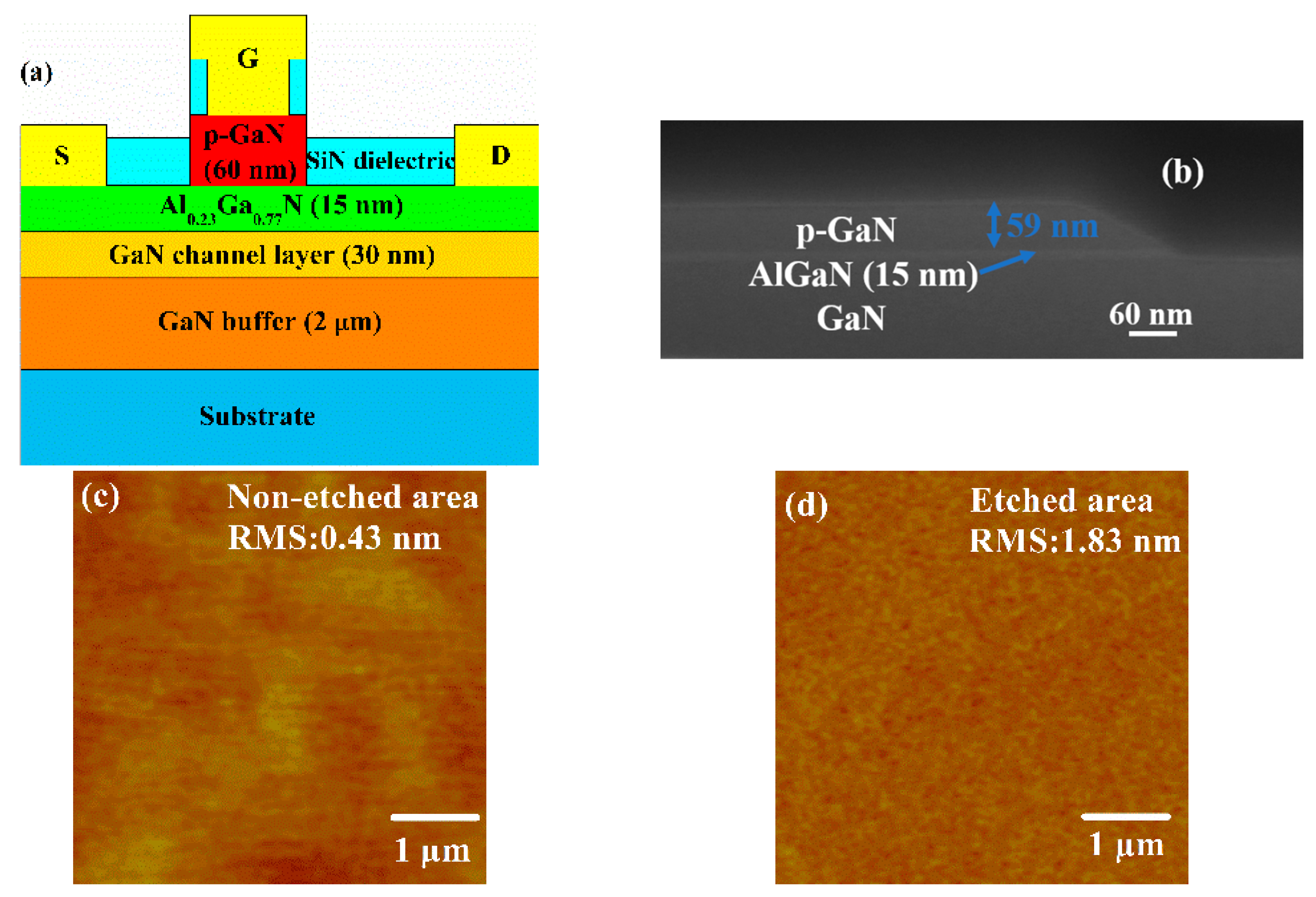
2. Device Structure
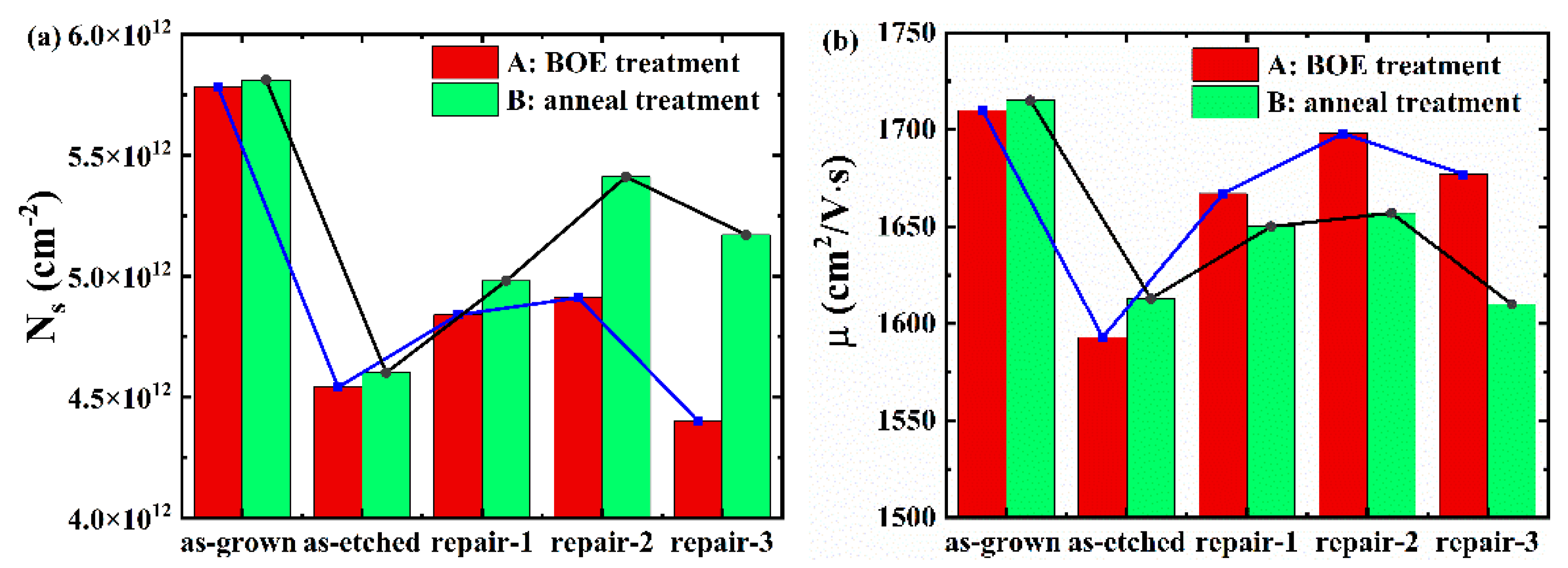
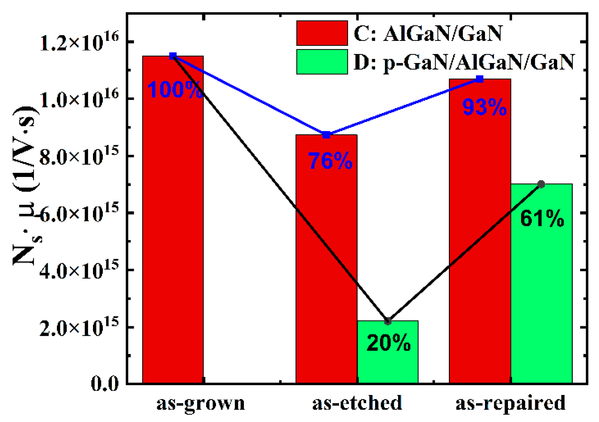
3. Results and Discussion
4. Conclusions
Author Contributions
Funding
Conflicts of Interest
References
- Jorudas, J.; Šimukovič, A.; Dub, M.; Sakowicz, M.; Prystawko, P.; Indrišiunas, S.; Kovalevskij, V.; Rumyantsev, S.; Knap, W.; Kašalynas, I. AlGaN/GaN on SiC devices without a GaN buffer layer: Electrical and noise characteristics. Micromachines 2020, 11, 1131. [Google Scholar] [CrossRef]
- Chen, K.J.; Haberlen, O.; Lidow, A.; Tsai, C.L.; Ueda, T.; Uemoto, Y.; Wu, Y. GaN-on-Si power technology: Devices and applications. IEEE Trans. Electron Devices 2017, 64, 779–795. [Google Scholar] [CrossRef]
- Millan, J.; Godignon, P.; Perpina, X.; Perez-Tomas, A.; Rebollo, J. A survey of wide bandgap power semiconductor devices. IEEE Trans. Power Electr. 2014, 29, 2155–2163. [Google Scholar] [CrossRef]
- Hilt, O.; Bahat-Treidel, E.; Knauer, A.; Brunner, F.; Zhytnytska, R.; Würfl, J. High-voltage normally off GaN power transistors on SiC and Si substrates. MRS Bull. 2014, 40, 418–424. [Google Scholar] [CrossRef]
- Liu, Y.; Yu, Q.; Du, J. Simulation design of a high-breakdown-voltage p-GaN-gate GaN HEMT with a hybrid AlGaN buffer layer for power electronics applications. J. Comput. Electron. 2020, 19, 1527. [Google Scholar] [CrossRef]
- Kim, H.; Heo, S.; Cha, H. Effective channel mobility of AlGaN/GaN-on-Si recessed- MOS-HEMTs. J. Semicond. Tech. Sci. 2016, 16, 867–872. [Google Scholar] [CrossRef] [Green Version]
- Li, G.; Li, X.; Zhao, J.; Yan, F.; Zhua, Q.; Gao, X. Design principle for a p-type oxide gate layer on AlGaN/GaN toward normally-off HEMTs: Li-doped NiO as a model. J. Mater. Chem. C 2020, 3. [Google Scholar] [CrossRef]
- Chen, Y.; Feng, J.; Wang, J.; Xu, X.; He, Z.; Li, G.; Lei, D.; Chen, Y.; Huang, Y. Degradation behavior and mechanisms of e-mode GaN HEMTs with p-GaN gate under reverse electrostatic discharge stress. IEEE Trans. Electron Devices 2020, 67, 566–570. [Google Scholar] [CrossRef]
- Saito, W.; Takada, Y.; Kuraguchi, M.; Tsuda, K.; Omura, I. Recessed-gate structure approach toward normally off high-voltage AlGaN/GaN HEMT for power electronics applications. IEEE Trans. Electron Devices 2006, 53, 356–362. [Google Scholar] [CrossRef]
- Liu, H.; Lin, C.; Hsu, W.; Lee, C.; Chiang, M.; Sun, W.; Wei, S.; Yu, S. Integration of gate recessing and in situ Cl- doped Al2O3 for enhancement-mode AlGaN/GaN MOS HEMTs fabrication. IEEE Electron Device Lett. 2017, 38, 91–94. [Google Scholar] [CrossRef]
- Kim, H.; Han, S.; Jang, W.; Cho, C.; Seo, K.; Oh, J.; Cha, H. Normally-off GaN-on-Si misfet using pecvd SiON gate dielectric. IEEE Electron Device Lett. 2017, 38, 1090–1093. [Google Scholar] [CrossRef]
- Uemoto, Y.; Hikita, M.; Ueno, H.; Matsuo, H.; Ishida, H.; Yanagihara, M.; Ueda, T.; Tanaka, T.; Ueda, D. Gate injection transistor (GIT)—a normally-off AlGaN/GaN power transistor using conductivity modulation. IEEE Trans. Electron Devices 2007, 54, 3393–3399. [Google Scholar] [CrossRef]
- Hao, R.; Fu, K.; Yu, G.; Li, W.; Yuan, J.; Song, L.; Zhang, Z.; Sun, S.; Li, X.; Cai, Y.; et al. Normally-off p-GaN/AlGaN/GaN high electron mobility transistors using hydrogen plasma treatment. Appl. Phys. Lett. 2016, 109, 152106. [Google Scholar] [CrossRef]
- Yu, C.; Hsu, C.; Wu, M.; Hsu, W.; Chuang, C.; Liu, J. Improved DC and RF performance of novel mis p-GaN-gated HEMTs by gate-all-around structure. IEEE Electron Device Lett. 2020, 41, 673–676. [Google Scholar] [CrossRef]
- Cai, Y.; Zhou, Y.; Chen, K.; Lau, K. High-performance enhancement-mode AlGaN/GaN HEMTs using fluoride-based plasma treatment. IEEE Electron Device Lett. 2005, 26, 435–437. [Google Scholar] [CrossRef]
- Tang, Z.; Jiang, Q.; Lu, Y.; Huang, S.; Yang, S.; Tang, X.; Chen, K. 600-V normally off SiNx/AlGaN/GaN MIS-HEMT with large gate swing and low current collapse. IEEE Electron Device Lett. 2013, 34, 1373–1375. [Google Scholar] [CrossRef]
- Mizutani, T.; Yamada, H.; Kishimoto, S.; Nakamura, F. Normally off AlGaN/GaN high electron mobility transistors with p-InGaN cap layer. J. Appl. Phys. 2013, 113, 034502. [Google Scholar] [CrossRef]
- Mizutani, T.; Ito, M.; Kishimoto, S.; Nakamura, F. AlGaN/GaN HEMTs with thin InGaN cap layer for normally off operation. IEEE Electron Device Lett. 2007, 28, 549–551. [Google Scholar] [CrossRef]
- Suzuki, A.; Choe, S.; Yamada, Y.; Otsuka, N.; Ueda, D. NiO gate GaN-based enhancement-mode hetrojunction field-effect transistor with extremely low on-resistance using metal organic chemical vapor deposition regrown Ge-doped layer. Jpn. J. Appl. Phys. 2016, 55, 121001. [Google Scholar] [CrossRef]
- Wan, L.; Sun, P.; Liu, X.; Chen, D.; Que, X.; Yao, S.; Li, G. A highly efficient method to fabricate normally-off AlGaN/GaN HEMTs with low gate leakage via Mg diffusion. Appl. Phys. Lett. 2020, 116, 023504. [Google Scholar] [CrossRef]
- Benkhelifa, F.; Müller, S.; Polyakov, V.; Ambacher, O. Normally-off AlGaN/GaN/AlGaN double heterostructure HETs with a thick undoped GaN gate layer. IEEE Electron Device Lett. 2015, 36, 905. [Google Scholar] [CrossRef]
- Tokuda, H.; Asubar, J.; Kuzuhara, M. Design considerations for normally-off operation in Schottky gate p-GaN/AlGaN/GaN HEMTs. Jpn. J. Appl. Phys. 2020, 59, 084002. [Google Scholar] [CrossRef]
- Zhou, Y.; Zhong, Y.; Gao, H.; Dai, S.; He, J.; Feng, M.; Zhao, Y.; Sun, Q.; Dingsun, A.; Yang, H. p-GaN Gate enhancement-mode HEMT through a high tolerance self-terminated etching process. IEEE J. Electron Devices Soc. 2017, 5, 340–346. [Google Scholar] [CrossRef]
- Grecoa, G.; Iucolanob, F.; Roccafortea, F. Review of technology for normally-off HEMTs with p-GaN gate. Mater. Sci. Semicond. Process. 2018, 78, 96–105. [Google Scholar] [CrossRef]
- Zhong, Y.; Zhou, Y.; Gao, H.; Dai, S.; He, J.; Feng, M.; Sun, Q.; Zhang, J.; Zhao, Y.; DingSund, A.; et al. Self-terminated etching of GaN with a high selectivity over AlGaN under inductively coupled Cl2/N2/O2 plasma with a low-energy ion bombardment. Appl. Surf. Sci. 2017, 420, 817. [Google Scholar] [CrossRef]
- Fan, Q.; Chevtchenko, S.; Ni, X.; Cho, S.J.; Yun, F.; Morkoç, H. Reactive ion etch damage on GaN and its recovery. J. Vac. Sci. Technol. B 2006, 24, 1197–1201. [Google Scholar] [CrossRef]
- Chiu, H.; Chang, Y.; Li, B.; Wang, H.; Kao, H.; Hu, C.; Xuan, R. High-performance normally off p-GaN gate HEMT with composite AlN/Al0.17Ga0.83N/Al0.3Ga0.7N barrier layers design. IEEE J. Electron Devices Soc. 2018, 6, 201–206. [Google Scholar] [CrossRef]
- Nuttinck, S.; Gebara, E.; Laskar, J.; Harris, H. Study of self-heating effects, temperature-dependent modeling, and pulsed Load–pull measurements on GaN HEMTs. IEEE Trans. Microw. Theory Tech. 2001, 49, 2413–2420. [Google Scholar] [CrossRef]
- Hwang, I.; Kim, J.; Choi, H.S.; Choi, H.; Lee, J.; Kim, K.; Park, J.; Lee, J.; Ha, J.; Oh, J.; et al. p-GaN gate HEMTs with tungsten gate metal for high threshold voltage and low gate current. IEEE Electron Device Lett. 2013, 34, 202–204. [Google Scholar] [CrossRef]
- Hwang, I.; Oh, J.; Choi, H.S.; Kim, J.; Choi, H.; Kim, J.; Chong, S.; Shin, J.; Chung, U. Source-connected p-GaN gate HEMTs. for increased threshold voltage. IEEE Electron Device Lett. 2013, 34, 605–607. [Google Scholar] [CrossRef]


| Main Research Institute | Structural Parameters (μm) | Vth (V) | Vgs, max (V) | Ron (Ω·mm) | Id, max (mA/mm) |
|---|---|---|---|---|---|
| Our work | Lg = 3, Lgs = 5, Lgd = 10 | 1.6 | 7 | 23 | 153 |
| National Tsing Hua University [14] | Lg = 1, Lgs = 1, Lgd = 3 | 0.5 | 5 | 8.2 | 215.9 |
| Chang-Gung University [27] | Lg = 3, Lgs = 2, Lgd = 7 | 2.1 | 8 | 5.65 | 272 |
| Samsung [29] | Lg = 4, Lgs = 2, Lgd = 12 | 1.23 | 7 | 14 | 230 |
| Samsung [30] | Lg = 4, Lgs = 2, Lgd = 9 | 0.93 | 8 | 16 | 309 |
Publisher’s Note: MDPI stays neutral with regard to jurisdictional claims in published maps and institutional affiliations. |
© 2021 by the authors. Licensee MDPI, Basel, Switzerland. This article is an open access article distributed under the terms and conditions of the Creative Commons Attribution (CC BY) license (http://creativecommons.org/licenses/by/4.0/).
Share and Cite
Niu, D.; Wang, Q.; Li, W.; Chen, C.; Xu, J.; Jiang, L.; Feng, C.; Xiao, H.; Wang, Q.; Xu, X.; et al. The Influence of the Different Repair Methods on the Electrical Properties of the Normally off p-GaN HEMT. Micromachines 2021, 12, 131. https://doi.org/10.3390/mi12020131
Niu D, Wang Q, Li W, Chen C, Xu J, Jiang L, Feng C, Xiao H, Wang Q, Xu X, et al. The Influence of the Different Repair Methods on the Electrical Properties of the Normally off p-GaN HEMT. Micromachines. 2021; 12(2):131. https://doi.org/10.3390/mi12020131
Chicago/Turabian StyleNiu, Di, Quan Wang, Wei Li, Changxi Chen, Jiankai Xu, Lijuan Jiang, Chun Feng, Hongling Xiao, Qian Wang, Xiangang Xu, and et al. 2021. "The Influence of the Different Repair Methods on the Electrical Properties of the Normally off p-GaN HEMT" Micromachines 12, no. 2: 131. https://doi.org/10.3390/mi12020131