
Comparison of PDMS and NOA Microfluidic Chips: Deformation, Roughness, Hydrophilicity and Flow Performance

 , , and
Abstract
:1. Introductions
2. Materials and Methods
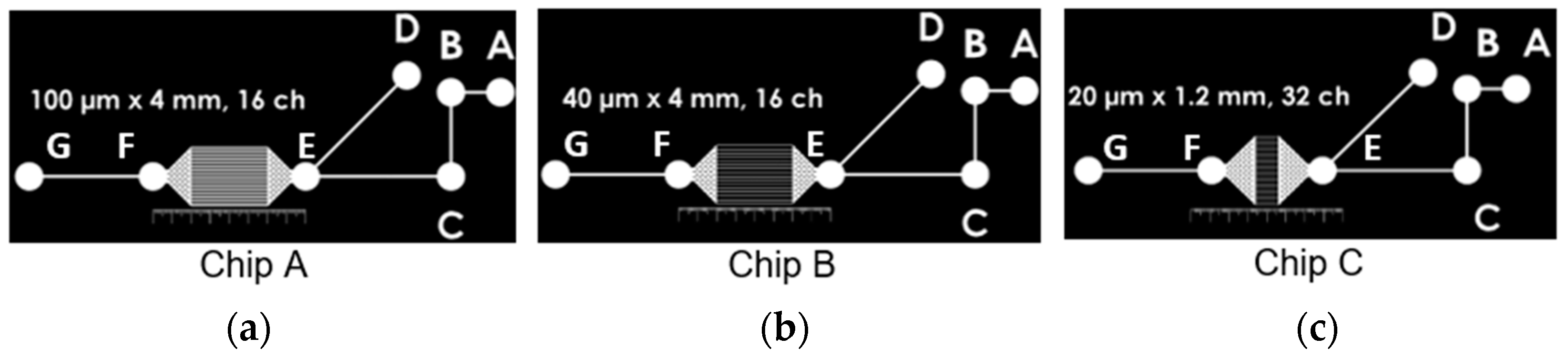
2.1. Microfluidic Devices Geometry
2.2. Manufacturing
2.2.1. SU-8 Wafer
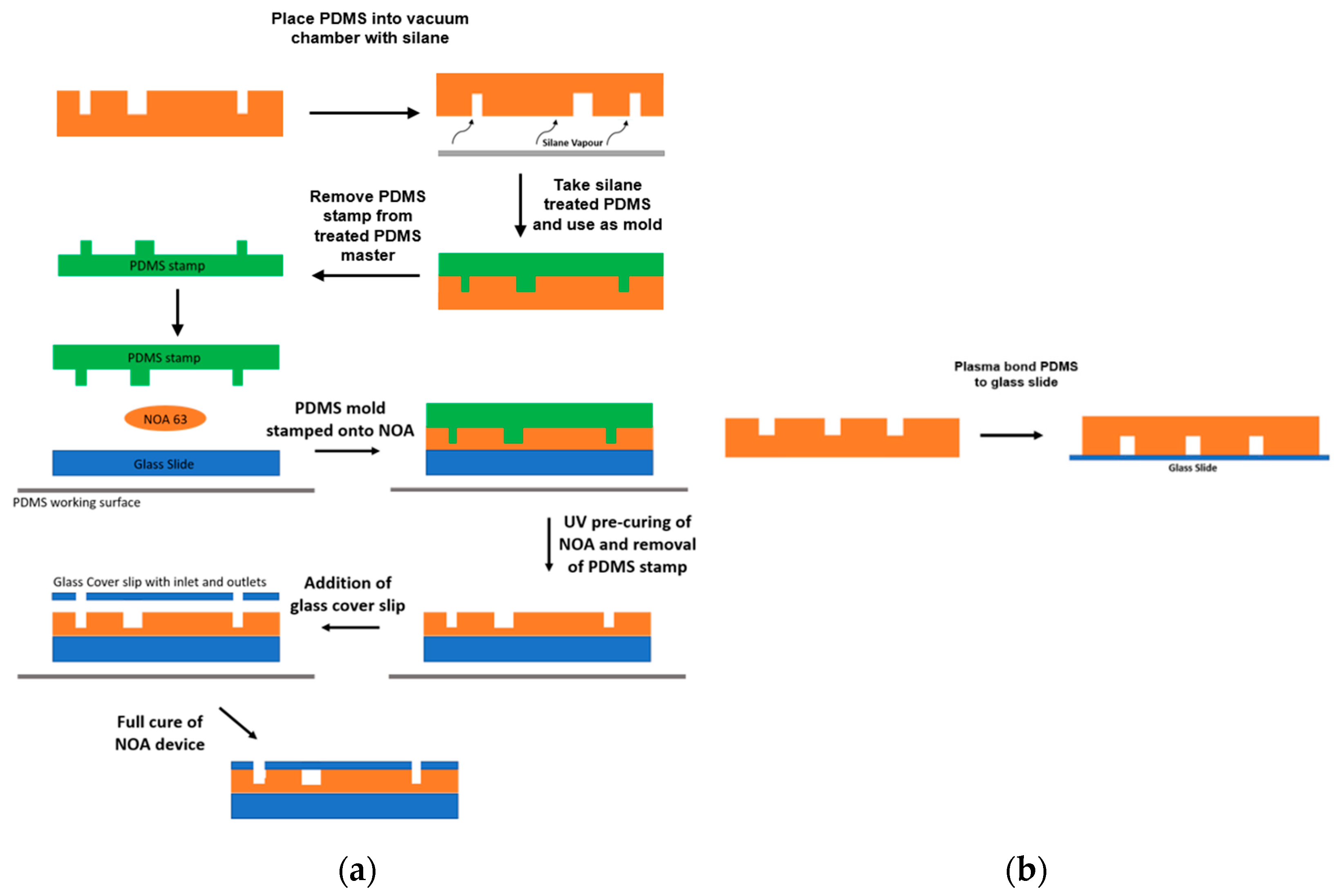
2.2.2. NOA Device
2.2.3. PDMS Device
2.3. Surface Roughness
2.4. Tensile Strength Test
2.5. Channels Width Deformation
2.6. Contact Angle
2.7. Experimental Setup
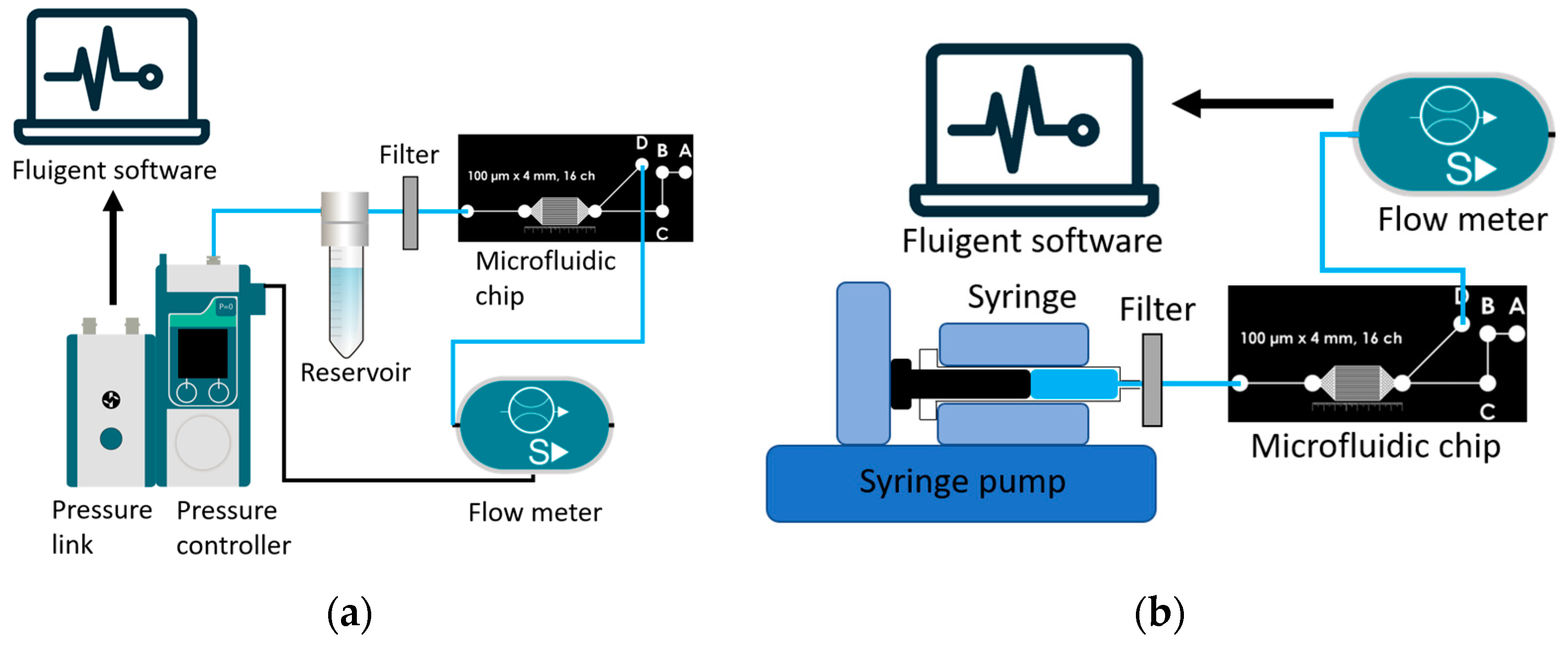
2.7.1. Pressure Controlled Setup for the Resistance of Microfluidic Devices
2.7.2. Flow Setup for the Characteristic Time of the Microfluidic Devices
2.8. Analysis
2.8.1. Theoretical and Hydraulic Resistance Estimation
2.8.2. Two-Element Resistance Compliance (RC) Hydraulic Circuit Model
2.8.3. Characteristic Time and Compliance
2.9. Statistical Analysis
3. Results
3.1. Mechanical Properties
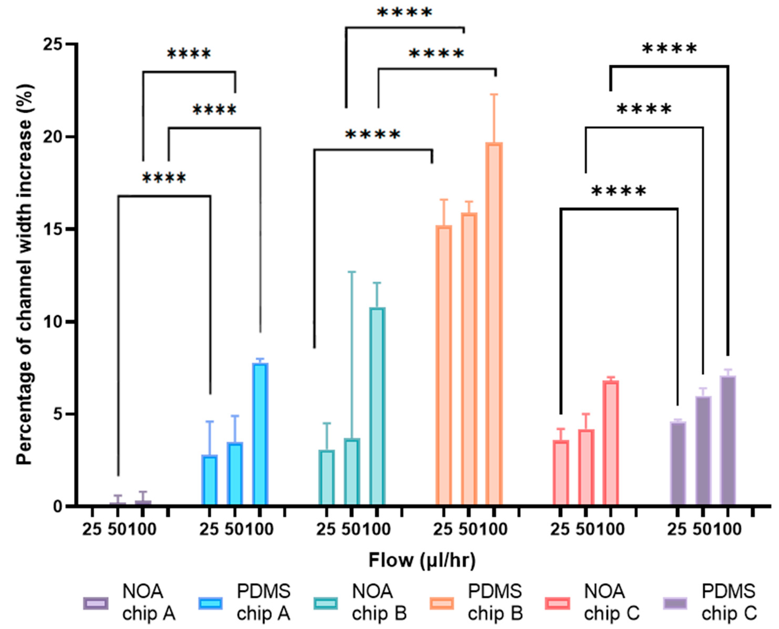
3.2. Channels Width Deformation
3.3. Contact Angle
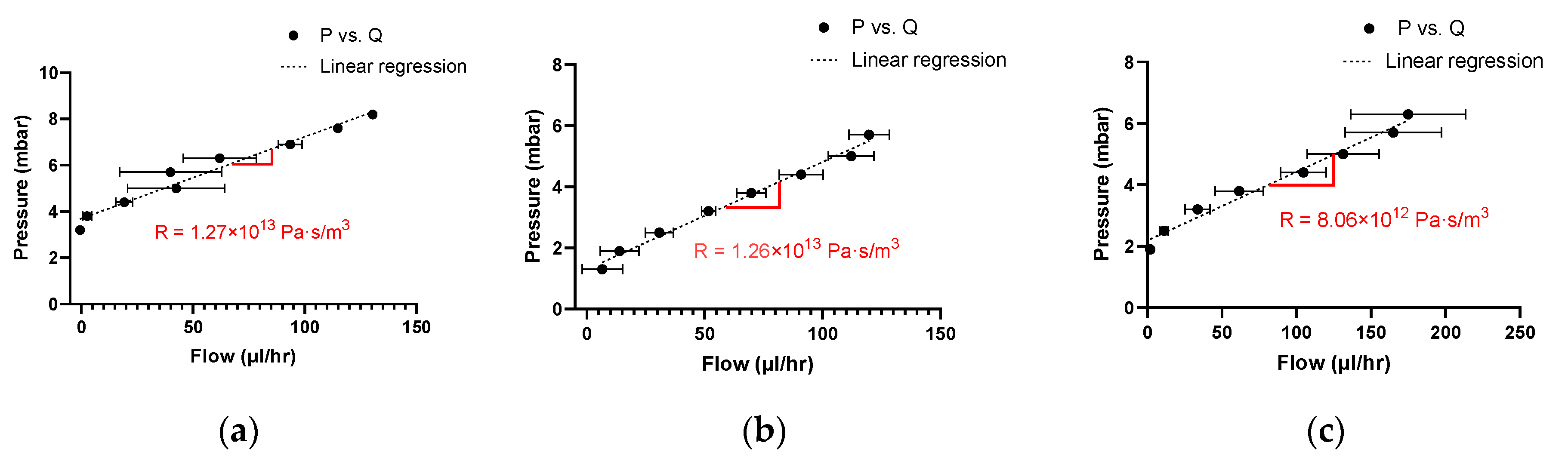
3.4. Resistance Estimation
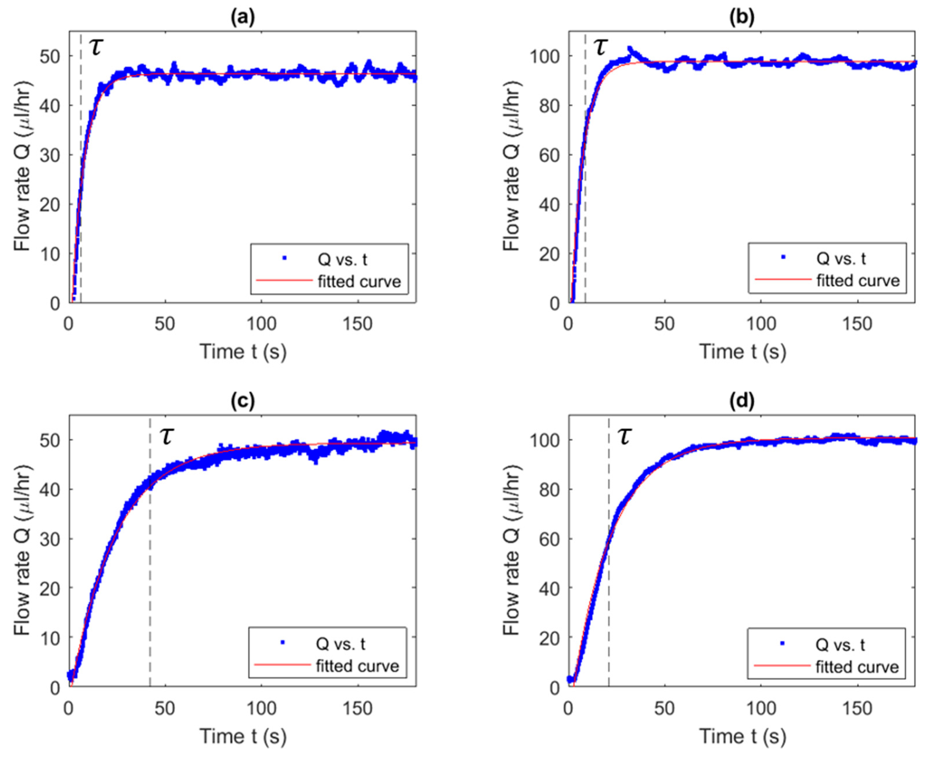
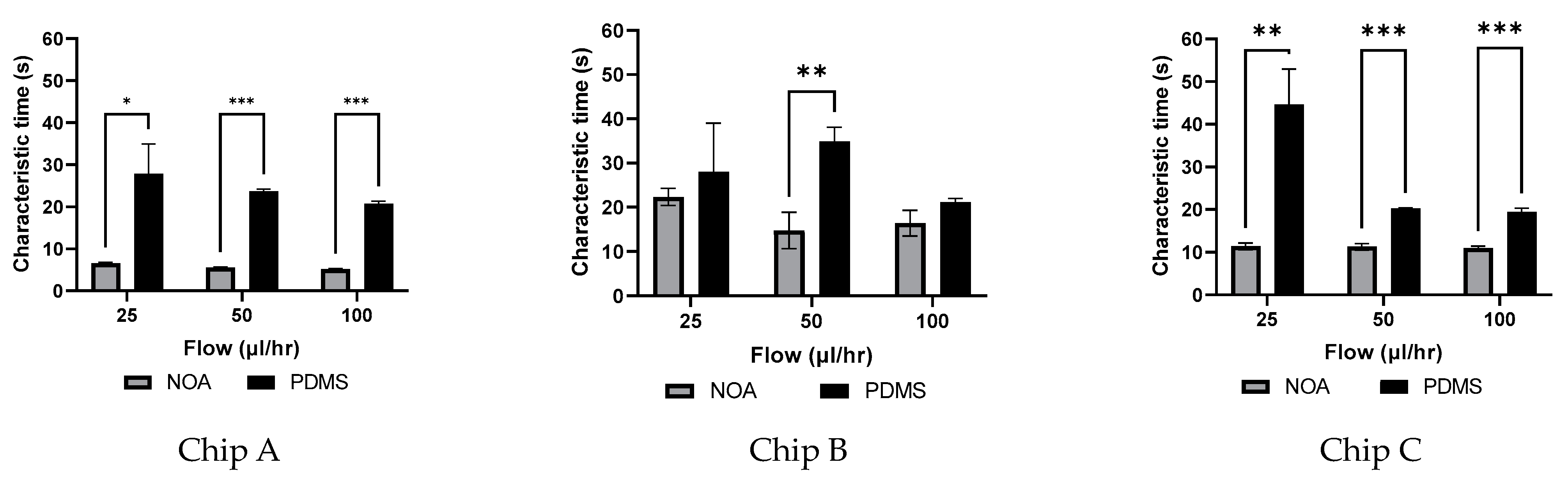
3.5. Characteristic Time Estimation
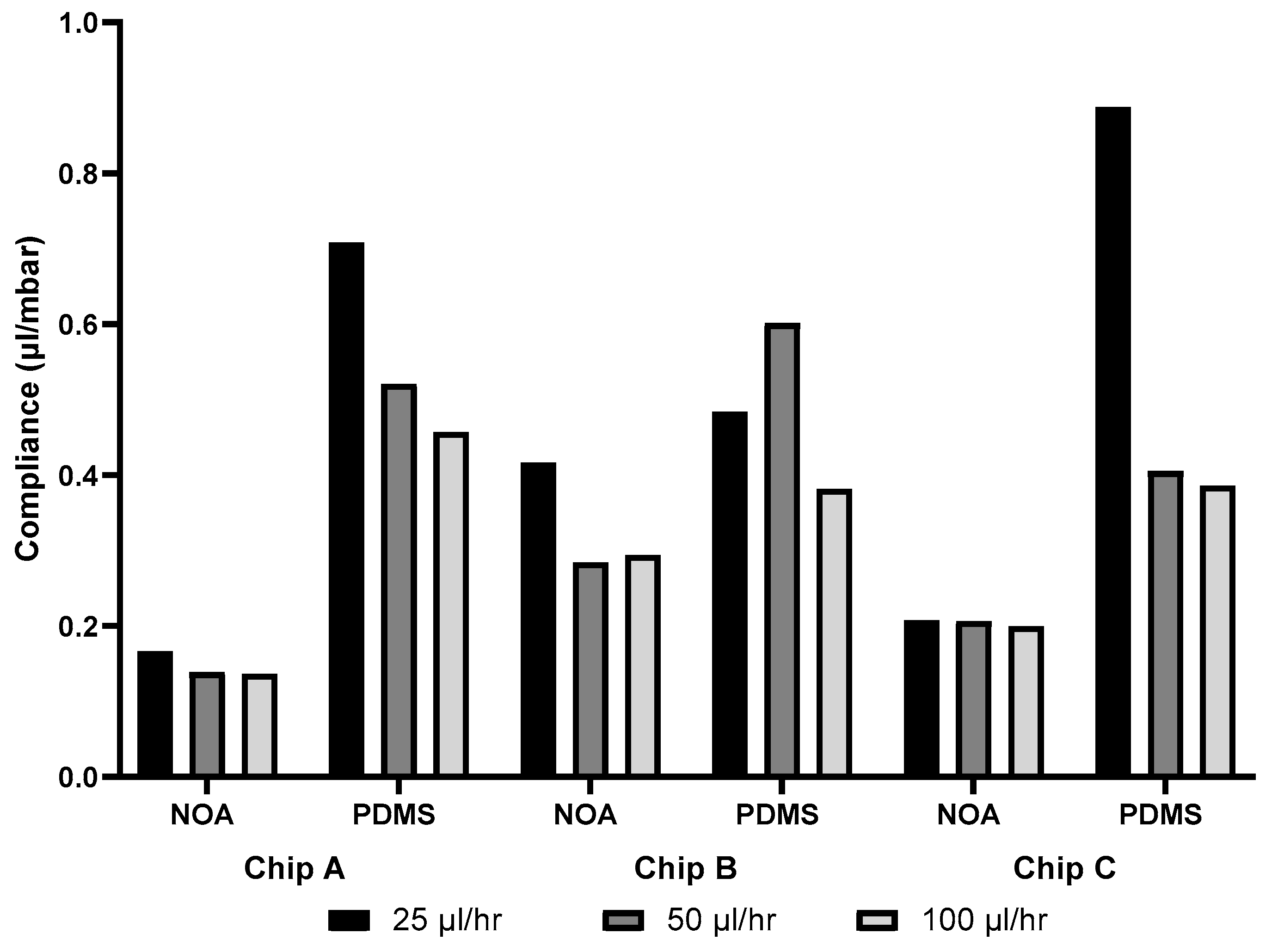
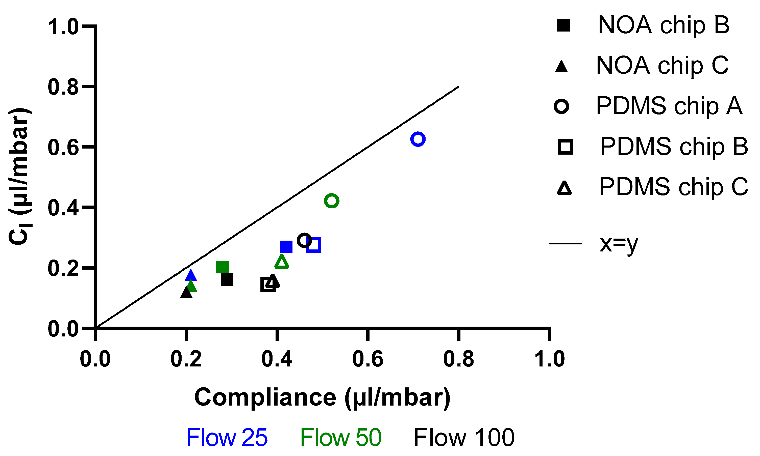
3.6. Compliance
4. Discussion
4.1. Material Properties
4.1.1. Surface Roughness and Young’s Modulus
4.1.2. Hydrophilicity/Hydrophobicity of Surface
4.2. Experimental Resistance
4.2.1. Channels Width Deformation
4.2.2. Dependency of Characteristic Time on Flow Rate
4.3. Flow Rate Measurement Uncertainty
4.4. Compliance
4.5. Anticipated Periodic Instability of the Output Flow
5. Conclusions
Author Contributions
Funding
Data Availability Statement
Acknowledgments
Conflicts of Interest
References
- McDonald, J.C.; Whitesides, G.M. Poly(dimethylsiloxane) as a Material for Fabricating Microfluidic Devices. ChemInform 2002, 33, 265. [Google Scholar] [CrossRef]
- Toepke, M.W.; Beebe, D.J. PDMS absorption of small molecules and consequences in microfluidic applications. Lab Chip 2006, 6, 1484–1486. [Google Scholar] [CrossRef]
- Hardy, B.S.; Uechi, K.; Zhen, J.; Kavehpour, H.P. The deformation of flexible PDMS microchannels under a pressure driven flow. Lab Chip 2009, 9, 935–938. [Google Scholar] [CrossRef]
- Gervais, T.; El-Ali, J.; Günther, A.; Jensen, K.F. Flow-induced deformation of shallow microfluidic channels. Lab Chip 2006, 6, 500–507. [Google Scholar] [CrossRef]
- Lee, K.S.; Ram, R.J. Plastic-PDMS bonding for high pressure hydrolytically stable active microfluidics. Lab Chip 2009, 9, 1618–1624. [Google Scholar] [CrossRef]
- Squires, T.M.; Quake, S.R. Microfluidics: Fluid physics at the nanoliter scale. Rev. Mod. Phys. 2005, 77, 977–1026. [Google Scholar] [CrossRef]
- Kirby, B.J. Micro- and Nanoscale Fluid Mechanics: Transport in Microfluidic Devices, 1st ed.; Cambridge University Press: Cambridge, UK, 2012; ISBN 978-0-521-11903-0. [Google Scholar]
- Beebe, D.J.; Mensing, G.A.; Walker, G.M. Physics and Applications of Microfluidics in Biology. Annu. Rev. Biomed. Eng. 2002, 4, 261–286. [Google Scholar] [CrossRef] [PubMed]
- Stone, H.; Stroock, A.; Ajdari, A. Engineering Flows in Small Devices: Microfluidics Toward a Lab-on-a-Chip. Annu. Rev. Fluid Mech. 2004, 36, 381–411. [Google Scholar] [CrossRef]
- El-Ali, J.; Sorger, P.K.; Jensen, K.F. Cells on chips. Nature 2006, 442, 403–411. [Google Scholar] [CrossRef]
- Liu, M.; Sun, J.; Sun, Y.; Bock, C.; Chen, Q. Thickness-dependent mechanical properties of polydimethylsiloxane membranes. J. Micromech. Microeng. 2009, 19, 035028. [Google Scholar] [CrossRef]
- Oertel, H. Biofluid Mechanics; Springer: New York, NY, USA, 2010; Volume 158, ISBN 978-1-4398-4518-9. [Google Scholar]
- Chayer, B.; Pitts, K.L.; Cloutier, G.; Fenech, M. Velocity measurement accuracy in optical microhemodynamics: Experiment and simulation. Physiol. Meas. 2012, 33, 1585. [Google Scholar] [CrossRef]
- Mehri, R.; Mavriplis, C.; Fenech, M. Design of a microfluidic system for red blood cell aggregation investigation. J. Biomech. Eng. 2014, 136, 064501. [Google Scholar] [CrossRef]
- Pitts, K.L.; Fenech, M. Micro-particle Image Velocimetry for Velocity Profile Measurements of Micro Blood Flows. J. Vis. Exp. 2013, 74, e50314. [Google Scholar] [CrossRef]
- Sim, J.H.; Moon, H.J.; Roh, Y.H.; Jung, H.W.; Bong, K.W. Fabrication of NOA microfluidic devices based on sequential replica molding. Korean J. Chem. Eng. 2017, 34, 1495–1499. [Google Scholar] [CrossRef]
- Dupont, E.P.; Luisier, R.; Gijs, M.A.M. NOA 63 as a UV-curable material for fabrication of microfluidic channels with native hydrophilicity. Microelectron. Eng. 2010, 87, 1253–1255. [Google Scholar] [CrossRef]
- Kim, H.; Yang, Y.; Kim, M.; Nam, S.W.; Lee, K.M.; Lee, N.Y.; Kim, Y.S.; Park, S. Simple Route to Hydrophilic Microfluidic Chip Fabrication Using an Ultraviolet (UV)-Cured Polymer. Adv. Funct. Mater. 2007, 17, 3493–3498. [Google Scholar] [CrossRef]
- Sollier, E.; Murray, C.; Maoddi, P.; Carlo, D.D. Rapid prototyping polymers for microfluidic devices and high pressure injections. Lab Chip 2011, 11, 3752–3765. [Google Scholar] [CrossRef]
- Rakesh, T.G.; Girisha, C.; Satish, V.T. A Review on the Effect of Surface Roughness and Liquid Slip on fluid flow in PDMS Microchannels. IOP Conf. Ser. Mater. Sci. Eng. 2021, 1189, 012021. [Google Scholar] [CrossRef]
- Pitts, K.L.; Abu-Mallouh, S.; Fenech, M. Contact angle study of blood dilutions on common microchip materials. J. Mech. Behav. Biomed. Mater. 2013, 17, 333–336. [Google Scholar] [CrossRef]
- Lee-Yow, N.; Pitts, K.L.; Fenech, M. Optically Clear Biomicroviscometer with Modular Geometry Using Disposable PDMS Chips. In Proceedings of the 2017 IEEE International Symposium on Medical Measurements and Applications (MeMeA), Rochester, MN, USA, 7–10 May 2017; IEEE: Rochester, MN, USA, 2017; pp. 72–77. [Google Scholar]
- MicroChem. “SU8_2035-2100.pdf”. Available online: https://www.seas.upenn.edu/~nanosop/documents/SU8_2035-2100.pdf (accessed on 26 October 2023).
- Chuang, Y.J.; Tseng, F.G.; Lin, W.K. Reduction of diffraction effect of UV exposure on SU-8 negative thick photoresist by air gap elimination. Microsyst. Technol. 2002, 8, 308–313. [Google Scholar] [CrossRef]
- Zhuang, G.; Kutter, J.P. Anti-stiction coating of PDMS moulds for rapid microchannel fabrication by double replica moulding. J. Micromech. Microeng. 2011, 21, 105020. [Google Scholar] [CrossRef]
- Khanafer, K.; Duprey, A.; Schlicht, M.; Berguer, R. Effects of strain rate, mixing ratio, and stress-strain definition on the mechanical behavior of the polydimethylsiloxane (PDMS) material as related to its biological applications. Biomed. Microdevices 2009, 11, 503–508. [Google Scholar] [CrossRef] [PubMed]
- Ye, X.; Liu, H.; Ding, Y.; Li, H.; Lu, B. Research on the cast molding process for high quality PDMS molds. Microelectron. Eng. 2009, 86, 310–313. [Google Scholar] [CrossRef]
- Johnston, I.D.; McCluskey, D.K.; Tan, C.K.L.; Tracey, M.C. Mechanical characterization of bulk Sylgard 184 for microfluidics and microengineering. J. Micromech. Microeng. 2014, 24, 035017. [Google Scholar] [CrossRef]
- Roh, C.; Lee, J.; Kang, C. The Deformation of Polydimethylsiloxane (PDMS) Microfluidic Channels Filled with Embedded Circular Obstacles under Certain Circumstances. Molecules 2016, 21, 798. [Google Scholar] [CrossRef]
- Tabeling, P. Introduction to Microfluidics; Oxford University Press (OUP): Oxford, UK, 2023. [Google Scholar]
- Tavoularis, S. Measurement in Fluid Mechanics. J. Fluids Struct. 2007, 23, 159–160. [Google Scholar] [CrossRef]
- NOA63. Available online: https://www.norlandprod.com/adhesives/noa%2063.html (accessed on 20 October 2023).
- Sotiri, I.; Tajik, A.; Lai, Y.; Zhang, C.; Kovalenko, E.; Nemr, C.; Ledoux, H.; Alvarenga, J.; Johnson, E.; Patanwala, H.; et al. Tunability of liquid-infused silicone materials for biointerfaces. Biointerphases 2018, 13, 06D401. [Google Scholar] [CrossRef]
- Gitlin, L.; Schulze, P.; Belder, D. Rapid replication of master structures by double casting with PDMS. Lab Chip 2009, 9, 3000–3002. [Google Scholar] [CrossRef] [PubMed]
- Xie, S.; Wu, J.; Tang, B.; Zhou, G.; Jin, M.; Shui, L. Large-Area and High-Throughput PDMS Microfluidic Chip Fabrication Assisted by Vacuum Airbag Laminator. Micromachines 2017, 8, 218. [Google Scholar] [CrossRef]
- Kang, C.; Roh, C.; Overfelt, R.A. Pressure-driven deformation with soft polydimethylsiloxane (PDMS) by a regular syringe pump: Challenge to the classical fluid dynamics by comparison of experimental and theoretical results. RSC Adv. 2014, 4, 3102–3112. [Google Scholar] [CrossRef]
- Li, Z.; Mak, S.Y.; Sauret, A.; Shum, H.C. Syringe-pump-induced fluctuation in all-aqueous microfluidic system implications for flow rate accuracy. Lab Chip 2014, 14, 744. [Google Scholar] [CrossRef] [PubMed]
- Zeng, W.; Jacobi, I.; Beck, D.J.; Li, S.; Stone, H.A. Characterization of syringe-pump-driven induced pressure fluctuations in elastic microchannels. Lab Chip 2014, 15, 1110. [Google Scholar] [CrossRef] [PubMed]


| Parallel Channels | |||
|---|---|---|---|
| Parameters | A | B | C |
| Width () (μm) | 100 | 40 | 20 |
| Height () (μm) | 100 | 100 | 100 |
| Length (L) (μm) | 4000 | 4000 | 1200 |
| Number of parallel channels | 16 | 16 | 32 |
| Tapered Channels | |||
| Width of entrance () (μm) | 500 | 500 | 500 |
| Width of exit () (μm) | 3100 | 3100 | 3740 |
| Height of channel (h) (μm) | 100 | 100 | 100 |
| Radius of micropillar () (μm) | 50 | 50 | 50 |
| Length of tapered channels (λ) (μm) | 1270 | 1270 | 1591 |
| Half distance between fibers (Δ) (μm) | 50 | 50 | 50 |
| Parameters | Inlet Channel (Ports GF) | Outlet Channel (Ports ED) | Outlet Channel (Ports EC) | Outlet Channel (Ports CB) | Outlet Channel (Ports BA) |
|---|---|---|---|---|---|
| Width () (μm) | 100 | 100 | 100 | 100 | 100 |
| Height () (μm) | 150 | 150 | 150 | 150 | 150 |
| Length (L) (μm) | 5000 | 6000 | 6129 | 2925 | 1104 |
| Sample | Pa (µm) | Pq (µm) | Experimental Young’s Modulus (MPa) | Literature Young’s Modulus (MPa) |
|---|---|---|---|---|
| NOA63 | 1559 ± 77 | 1867 ± 98 | 1743 ± 173 | 1655 [32] |
| PDMS | 147 ± 4 | 169 ± 4 | 2 ± 0.2 | 1–3 [3,4,6] |
| Chip | Theoretical Resistance (1012 Pa·s/m3) | NOA63 Experimental Resistance (1012 Pa·s/m3) | PDMS Experimental Resistance (1012 Pa·s/m3) |
|---|---|---|---|
| A | 4.78–4.79 | 4.64 | 4.54 |
| B | 5.34–5.66 | 5.44 | 5.65 |
| C | 5.09–5.75 | 5.44 | 5.04 |
Disclaimer/Publisher’s Note: The statements, opinions and data contained in all publications are solely those of the individual author(s) and contributor(s) and not of MDPI and/or the editor(s). MDPI and/or the editor(s) disclaim responsibility for any injury to people or property resulting from any ideas, methods, instructions or products referred to in the content. |
© 2023 by the authors. Licensee MDPI, Basel, Switzerland. This article is an open access article distributed under the terms and conditions of the Creative Commons Attribution (CC BY) license (https://creativecommons.org/licenses/by/4.0/).
Share and Cite
Turcitu, T.; Armstrong, C.J.K.; Lee-Yow, N.; Salame, M.; Le, A.V.; Fenech, M. Comparison of PDMS and NOA Microfluidic Chips: Deformation, Roughness, Hydrophilicity and Flow Performance. Micromachines 2023, 14, 2033. https://doi.org/10.3390/mi14112033
Turcitu T, Armstrong CJK, Lee-Yow N, Salame M, Le AV, Fenech M. Comparison of PDMS and NOA Microfluidic Chips: Deformation, Roughness, Hydrophilicity and Flow Performance. Micromachines. 2023; 14(11):2033. https://doi.org/10.3390/mi14112033
Chicago/Turabian StyleTurcitu, Tatiana, Curtis J. K. Armstrong, Niko Lee-Yow, Maya Salame, Andy Vinh Le, and Marianne Fenech. 2023. "Comparison of PDMS and NOA Microfluidic Chips: Deformation, Roughness, Hydrophilicity and Flow Performance" Micromachines 14, no. 11: 2033. https://doi.org/10.3390/mi14112033