

Modeling and Validation of Total Ionizing Dose Effect on the TSVs in RF Microsystem

1
School of Microelectronics, Xidian University, Xi’an 710071, China
2
China Academy of Aerospace Standardization and Product Assurance, Beijing 100071, China
*
Author to whom correspondence should be addressed.
Micromachines 2023, 14(6), 1180; https://doi.org/10.3390/mi14061180
Submission received: 3 April 2023
/
Revised: 27 May 2023
/
Accepted: 30 May 2023
/
Published: 31 May 2023
(This article belongs to the Special Issue Selected Papers from the 8th International Conference on Sensors and Electronic Instrumentation Advances (SEIA' 2022))
Abstract
:Radio frequency (RF) systems utilizing through-silicon vias (TSVs) have been widely used in the aerospace and nuclear industry, which means that studying the total ionizing dose (TID) effect on TSV structures has become necessary. To investigate the TID effect on TSV structures, a 1D TSV capacitance model was established in COMSOL Multiphysics (COMSOL), and the impact of irradiation was simulated. Then, three types of TSV components were designed, and an irradiation experiment based on them was conducted, to validate the simulation results. After irradiation, the S21 degraded for 0.2 dB, 0.6 dB, and 0.8 dB, at the irradiation dose of 30 krad (Si), 90 krad (Si), 150 krad (Si), respectively. The variation trend was consistent with the simulation in the high-frequency structure simulator (HFSS), and the effect of irradiation on the TSV component was nonlinear. With the increase in the irradiation dose, the S21 of TSV components deteriorated, while the variation of S21 decreased. The simulation and irradiation experiment validated a relatively accurate method for assessing the RF systems’ performance under an irradiation environment, and the TID effect on structures similar to TSVs in RF systems, such as through-silicon capacitors.
1. Introduction
The radio frequency (RF) circuit is an essential part of RF systems, which have been widely used in the corresponding wireless area and RF identification, including fifth-generation wireless systems, artificial intelligence, aerospace research, and so on. The RF chip plays an essential role in wireless correspondence. For example, RF transceivers minimize the radio system, and even the most conservative of the space industries identify the benefits of RF chips. With the growing markets for, and improvements in, circuit manufacturing, new technologies such as three-dimensional (3D) integration technology have been applied to RF chips. By using 3D integration technology, RF systems’ delay and power consumption can be decreased; thus, system-on-chip (SOC) with complex functions can be realized.
The effect of irradiation on RF systems cannot be ignored. Researchers are studying the impact of irradiation on complementary metal–oxide–semiconductor-integrated circuits (CMOS-ICs), metal–oxide–semiconductor field-effect transistors (MOSFETs), and the whole RF system. When studying through-silicon vias (TSVs), most researchers focus on the electrical, thermal, and stress issues of TSVs. It becomes necessary to understand the radiation resistance reliability of TSVs. In 2013, the combined effects of the total ionizing dose (TID) effect, process corners, and the temperature, on high-frequency RF circuits’ performance, were presented [1]. In 2014, back-channel implantation was introduced as an effective way to suppress the radiation-induced coupling effect [2]. In 2017, a comprehensive charge-based predictive model of interface and oxide-trapped charges in undoped symmetric long-channel double-gate MOSFETs was developed, and integrated well into all regions of operation [3]. In 2020, a new radiation-tolerant IC design method using an I-gate structure was proposed, and a device based on it was designed and fabricated in the standard CMOS process [4]. In 2021, J. Feng studied the TID effect on an 8-transistor global-shutter-exposure complementary metal–oxide–semiconductor image sensor (CIS) within a star sensor [5]. The effects of the TID Effect on CMOS-ICs are well studied [6,7,8,9,10,11,12,13]. Regarding the research on TSVs, Li Yanruoyue and his team used the finite element method to determine the effect of the thickness of the SiO2 layer on the distribution of thermal stress [14]. In 2021, Kan Li studied the TID effect in advanced bulk nMOS and pMOS FinFETs with nearby SiO2/HfO2 gate dielectrics and TSVs. The threshold voltage shifts introduced by TSVs are less than 25 mV [15]. Thus, the pulse frequency, oxide thickness, the radius of TSVs, and the space between TSVs have been investigated [16,17,18].
Our previous paper [19] briefly introduced the simulation in COMSOL Multiphysics (COMSOL) [20], and our analysis based on experimentation. Our current research expanded on this basis, and presented more detail. Firstly, the structure and characteristics of TSVs were introduced. Secondly, the recommended method for finite element analysis was utilized in the investigation, and TSV models were developed. Then, three types of TSV components were designed and, based on them, an irradiation experiment was designed. After the irradiation experiment, the scattering parameters (S-parameters) of TSV components were measured, while the S-parameters of three types of TSV components were also simulated in a high-frequency structure simulator (HFSS) [21]. Following all of this, the results were analyzed and discussed, and our conclusions were drawn.
2. Theoretical Analysis
2.1. Structure of TSVs
Conventional TSVs are widely used in 3D ICs. Figure 1a,b show the longitudinal section and the cross section of a conventional TSV biased in the depletion regions. The material used for the TSV core is copper, with an annular dielectric barrier typically of silicon dioxide (SiO2) surrounding the copper cylinder. The whole structure is built on a p-type silicon substrate.
2.2. TID Effect on SiO2
The TID effect impacts TSV in the following ways: the radiation induces excess electron–hole pairs in the insulators (Equation (1) shows the number of pairs generated per unit dose in a given oxide volume); the electrons are more mobile, and they exit, leaving hole charges; the hole charge is trapped in the oxide in deep-level traps, moving very slowly by hopping from trap to trap.
where q = 1.6 × 10¹² eV·erg−1, refers to the elementary charge; Ep = 17 eV−1, refers to the mean ionization energy of the SiO2; rho = 2.2 g·cm−3, refers to the material density of SiO2.
Trapped holes get trapped in deep traps very close to the interface, altering the surface-carrier concentrations in the silicon. Holes and protons that move to the interface create additional defects. This trapped charge, and these interface defects, change the local carrier population, and reduce the carrier lifetime, near the surface of the SiO2–silicon interface.
The total density of positive fixed charge accumulated in the oxide can be calculated as a function of the total dose (D) using Equation (2):
In the equation, tox is the thickness of the oxide layer. fot is the hole-trapping efficiency, and it can be assumed as a fitting parameter that should be empirically determined. fy(Eox) is the fractional yield. It depends on the electric field in the oxide at the moment of irradiation, and can be calculated using Equation (3):
where E0 = 0.1 V/cm, m = 0.7, and E1 = 0.55 MV/cm, for Co-60 γ-ray sources [22]. As seen in Equation (3), ΔNot is proportional to the thickness of the oxide layer. Therefore, for TSV structures with thick oxide layers, the total density of positive fixed charge caused by radiation can be ignored.
The charge in the oxide can be calculated using Equation (4):
2.3. The Capacitance of TSVs after Irradiation
For a TSV with length h, Cox can be expressed by the cylindrical capacitor equation:
where εox is the permittivity of SiO2; rTSV is the radius of the TSV conductor; rox is the radius of the outer surface of the TSV oxide liner.
Then, the depletion capacitance of a single TSV can be obtained by:
where φ(rox) is the surface potential at the Si–SiO2 interface (r = rox), which can be calculated with the doping concentration of the acceptor ions, the thickness of the depletion, and rox.
Then, the total capacitance of TSV CTSV is the series combination of the oxide and the depletion capacitance, and it can be expressed as:
The section discussed the TID effect on SiO2 and the capacitance of TSV after irradiation, laid the foundation for the modeling of TSV structures, and provided a simulation of the TID effect on TSV structures.
3. Modeling of TSV Structures and Simulation
3.1. Modeling of TSV Structures
The model of the conventional TSV structure was developed in COMSOL, as shown in Figure 2. The main structure consists of four essential parts: the conductive filling layer, the oxide insulating layer, the p-type silicon substrate, and the outermost shielding copper layer. The diameter of the TSV is 5 microns, and the inner insulation layer thickness is 0.5 microns.
It is assumed that charge density is similar within the lamellar at the same height in a steady state. To simplify the model, a perpendicular plane is taken in the axial direction of the TSV. Furthermore, it can be considered that the capacitance between the TSV core layer and the p-type substrate is equal everywhere along the radial direction. Therefore, the part along any radial direction can be modeled. In COMSOL, the semiconductor interface is chosen. First, a line segment and two endpoints are set to represent the structure of the inner core layer. The left endpoint is set as a thin insulating gate, whose thickness is dox, and the surface charge density rhos_ox; and the right endpoint represents the ideal ohmic contact.
3.2. Simulation and Analysis
To analyze the effect of irradiation on TSV capacitance, CV curves under different radiation doses are simulated at low and high frequencies. Furthermore, to exclude the influence of oxide layer thickness, and substrate doping concentration, it is necessary to study their effects on TSV capacitance.
3.2.1. Effect of Irradiation on TSV Capacitance
The CV curves of the TSV capacitance are simulated with a p-type substrate concentration of , oxide thickness of 2.5 microns, frequency of 0.0001 Hz and Hz, and a total dose of , and , in turn.
Figure 3a shows the CV curves at low frequencies, at which the capacity of TSV is in the inverse zone. Figure 3b shows the CV curves at high frequencies, under which the inverse zone cannot form. In both Figures, after TSV is irradiated, the CV curves of the TSV capacitor drift to the left, and the higher the irradiation dose is, the more the CV curves drift to the left.
TSV is usually biased at the accumulation zone to avoid the volatility of capacitance value when used in RF chips. After radiation, the TSV capacitance enters the inverse zone at the lower voltage at both low and high frequencies.
According to Equation (5), Cox is determined by the permittivity εox, the length of TSV h, the radius of oxide layer rox, and the TSV core rTSV. In the simulation and the experiment, the dimension of the TSV is constant. According to the analysis in Section 2.3, the irradiation would affect the oxide charge and permittivity of SiO2, leading to the increase in TSV capacitance.
3.2.2. Effect of Oxide Thickness on Irradiated Capacitance
In the simulation, the substrate doping concentration is set as , the oxide layer is 200 nm, 1.25 micron, and 2.5 micron, the operating frequency is 0.001 Hz and , the total irradiation dose D of 0 and . The simulation results are shown in Figure 4:
As shown in Figure 4a, at low frequencies, the voltage corresponding to the loss zone of the TSV capacitor is between 0 and 5 V. After the total irradiation dose of , the CV curves of TSV shift to the left, and the thicker the oxide layer is, the more pronounced the curve deviation is. At this point, TSV capacitance enters the inverse zone at the same operating voltage. At low frequencies, the capacitance at the inverse zone is significantly greater than that in the maximum depletion zone. When designing TSV working at low frequencies and in irradiation environments, the operating point of the TSV should be set in the accumulation zone, to avoid the degradation of the TSV’s performance, caused by its instability.
Figure 4b shows the CV curves of TSV capacitance at high frequencies. Before TSV is irradiated, the maximum depletion zone of the TSV capacitor is between 0 and 5 V. At this operating voltage, the TSV capacitor demonstrates the minimum capacitance, and a relatively stable value, which is beneficial for improving the device’s performance. When the thickness of the oxide layer increases, the accumulation area capacitance of TSV decreases, and the voltage value corresponding to the maximum depletion area width increases. After the TSV capacitance is irradiated, the CV curve of the TSV capacitor moves to the left. Under standard operating voltage (0 to 5 V), the TSV capacitor is in the inverse region, and the TSV capacitance will not change significantly.
3.2.3. Effect of Substrate Doping Concentration on TSV Capacitance after Irradiation
In the simulation, the thickness of the oxide layer is set as 2.5 microns, and the CV curves of TSV capacitance are simulated with substrate doping concentrations of and , as shown in Figure 5a,b.
Figure 5a shows the CV curves of TSV capacitance at low frequencies. For TSV operating at low frequencies, the capacitance in the maximum depletion zone increases with substrate doping concentration. The maximum capacitance is obtained when TSV capacitance is in the accumulation and inverse zones, which remain the same before and after irradiation. With different substrate doping concentrations, the CV curves shift to the left by roughly the same amount after irradiation. As with Section 4.2, reducing the substrate doping concentration leads to a smaller TSV capacitance in the maximum depletion zone.
At high frequencies, the substrate doping concentration determines the capacitance in the maximum depletion zone, and is not affected by the irradiation dose.
4. Irradiation Experiment and Analysis
4.1. Design of Irradiation Experiment
In RF chips utilizing 3D integration technology, the position of the TSV affects the transmission performance of the TSV components. Three types of TSV components were designed to avoid the effect of TSV positioning. Figure 6a–c show three types of TSV components.
Figure 6 shows two main differences among those three types: firstly, the number of redundant TSVs connected to the GND; and secondly, whether the two copper layers connected to the GND are combined. The copper layers connected to the GND are separated for type A, which owns twelve redundant TSVs. The copper layers are combined for type B, which owns six redundant TSVs. The copper layers are separated for type C, which owns fourteen redundant TSVs. The dimension sets of the TSVs will be introduced in Section 5. A total of nine TSV components of each type were manufactured, to prevent the contingency of irradiation experiments on TSV components. In the irradiation experiment, three levels of irradiation dose were set, which were 30 krad (Si), 90 krad (Si), and 150 krad (Si). The irradiation source was Co-60 γ-ray. The settings of the irradiation experiment are shown in Table 1.
Three TSV components of each type were used. During the irradiation experiment, the effect of the annealing strongly affected test results. In consideration of the time between the experiment and the testing, the TSV components were introduced into the irradiation environment according to the following order. Firstly, three components were exposed to irradiation in the dose of 150 krad (Si); then, after 20 min, three components were exposed to 90 krad (Si); finally, after a further 20 min, three components were exposed to 30 krad (Si). Then, 10 min later, all TSV components were taken from the irradiation environment for testing.
4.2. The Results Tested before and after Irradiation
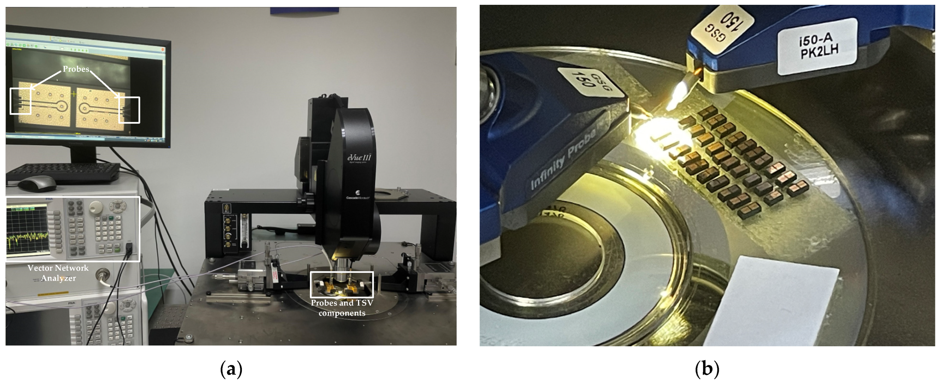
The testing environment is shown in Figure 7a,b. The equipment used for measuring the S-parameters of the TSV components were an eVue III digital imaging system (eVue III) and a vector network analyzer (VNA). During measuring, the eVue III enabled faster navigation, observation, and device measurements, which saved time. As shown in Figure 7a, two probes contact the ports of the TSV component. The probe has three ports; the middle transmits a signal and is connected to the signal TSV, and the other two ports connect to the ground. Then S-parameters are measured and shown in the VNA.
S-parameters describe the electrical behavior of linear electrical networks when undergoing various steady-state stimuli by electrical signals. Regarding a two-port system, S-parameters reflect transmission coefficients, demonstrate the transition performance of the TSV, and can be measured on the above types of equipment. For a two-port system, S21 and S12 represent the transmitting loss in the channel. The bigger S21 and S12 are, the worse the transmission performance of the TSV. S21 equals S12 because of the symmetrical structure of the TSV components shown in Figure 6.
The average S21 variation of the three types is shown in Figure 8a–c. The black, red, and green curves show the average S21 parameter variation of the three types, at the dose of 30 Krad (Si), 90 Krad (Si), and 150 Krad (Si).
4.3. Analysis Based on the Experiment and Measured Data
In the experiment, there were nine of each type of TSV component, making a total of 27 components. Some of the S21 of the same TSV components under the same irradiation dose were inconsistent in measurement. For example, at 10 GHz, the S21 of TSV components (type A) under the irradiation dose of 30 krad (Si) were measured after radiation. They degraded for 1.85 dB, 0.14 dB, and 0.44 dB, respectively. Under the irradiation dose of 90 krad (Si), the S21 of TSV components (type A) degraded for 0.86 dB, 0.06 dB, and 0.41 dB, respectively. The pressure and position of probes, process errors, and other manufacturing and testing factors caused the error. Testing a large number of TSV components and conducting statistical analysis helps to eliminate errors, whereas only 27 components have been experimented with, and tested, in the current research. The average value of the S21 parameter variation of the three components of the same type, at the same dose, was taken, to overcome the errors.
After taking the average, the variation trend of the S21 parameters became clear. The S21 of TSV components deteriorated after irradiation. As shown in Figure 8: with the increase in irradiation dose, the S21 parameters deteriorated more. At low frequencies, the average S21 variation at 30 Krad (Si), 90 Krad (Si), and 150 Krad (Si) were about 0.2 dB, 0.4 dB, and 0.9 dB. Although the quantities of experimental data are limited by the number of TSV components, three different types of TSV components all show the same trend. Moreover, as per the interpretation of Figure 3, because of the TID effect on TSV capacitance, the fixed charge accumulated in the oxide layer increased the capacity value at the inverse region, which caused the CV curves to drift to the left at both low and high frequencies.
According to the S21 simulated based on the model built in HFSS, the S21 curves behaved in the same manner after irradiation, which will be illustrated in the following sections.
5. Simulation Based on HFSS and Analysis
5.1. TSV Modeling in HFSS
HFSS is a full-wave 3D electromagnetic simulation software based on the finite element analysis of electromagnetic fields for microwave-engineering problems. Based on HFSS, the S-parameters of TSV components could be simulated.
According to the theoretical analysis, the total ionizing dose effect mainly affects the SiO2. Irradiation causes the increase in the charge in the oxide layer, and the closer that charges move to the Si–SiO2 interface, the greater the effect on the TSV oxide layer capacitance. According to Equation (5), the oxide layer capacitance is mainly determined by the relative permittivity of SiO2, the oxide layer thickness, the radius of the TSV copper core, and the length of the TSV. In the simulation, the dimensions of the TSV components were fixed, which means that the variation of TSV capacitance mainly reflected the relative permittivity of SiO2.
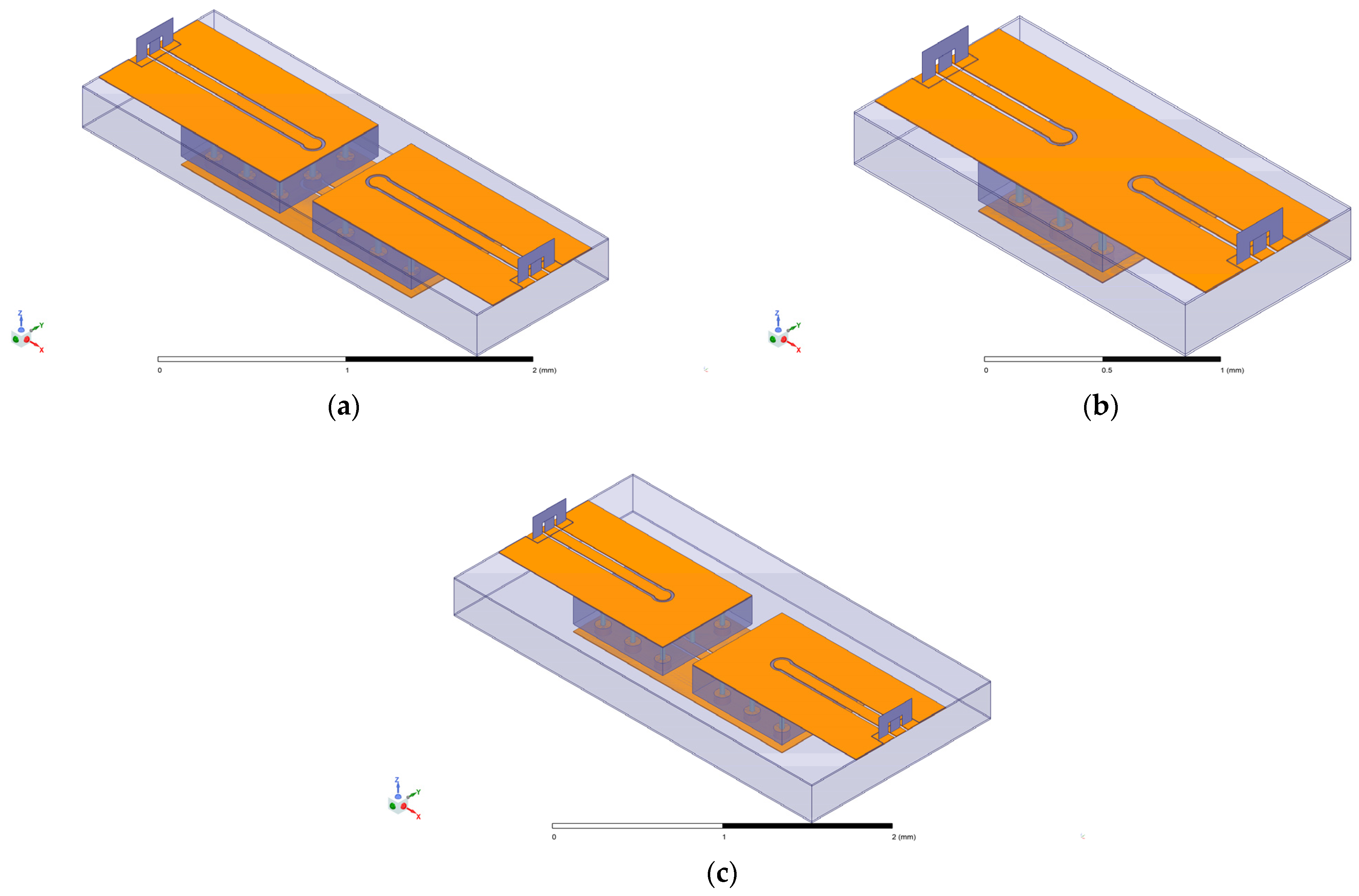
The simulation was based on type A in this section. In the TSV model of type A, the copper layers connected to the GND are separated; silicon, copper, and SiO2 constitute the main parts that affect the performance of the TSV component. There are twelve TSVs in the type A model, two of which are signal TSVs; the others are abundant TSVs. Each TSV has a bump beneath it, to bond the upper and lower chips. The core of the TSV is the copper column, which is surrounded by a SiO2 layer; the cuboid-shaped Si substrate encloses TSVs. Figure 9a,b show the flat view and the top view of the TSV model.
In the TSV model of type A, two TSVs are spaced 0.25 mm apart, the thickness of the oxide layer is 2.5 microns, the length of the TSV is 0.2 mm, the shape of the Si substrate is square, and the side length is 0.75 mm. The distance between the two signal TSVs is 0.5 mm. Modifying the size of materials will affect the simulation results, so establishing a relatively accurate model is necessary.
5.2. Simulation in HFSS
The relative permittivity of SiO2 varies from 4 to 20, and the simulation frequency range is set from 0 to 40 GHz. After the model is built and the boundary conditions are set, the S-parameters of the TSV model are simulated. The simulated S21 of the model of type A under different relative permittivity of SiO2 are as shown in Figure 10.
As shown in Figure 10, with the increasing relative permittivity of SiO2, the S21 curves move downward, and S21 deteriorates. The relative permittivity of SiO2 is set as 4, 8, 12, 16, and 20. The corresponding curves are black, red, blue, green, and yellow, and it is clear that from 5 to 25 GHz, the yellow curve is at the bottom, and the black curve is at the top.
5.3. Analysis Based on Simulation and Irradiation Experiment Results
As shown in Figure 10, the S21 of the TSV model of type A decreased rapidly with the increasing frequency within 5 GHz. In the 5–25 GHz range, the S21 of the TSV model of type A was nearly constant. When the frequency was greater than 25 GHz, S21 decreased with increasing frequency. The S21 curves show a similar trend under different relative permittivity of SiO2.
In the simulation, the relative permittivity of SiO2 was changed to simulate the situation after the TSV is irradiated. As shown in Figure 10, although the S21 curves show the same trend, the variation of S21 curves decreases with the exact change in relative permittivity of SiO2, as shown in Table 2. The data from the second to the fifth row represent the variation of S21 compared to the first row.
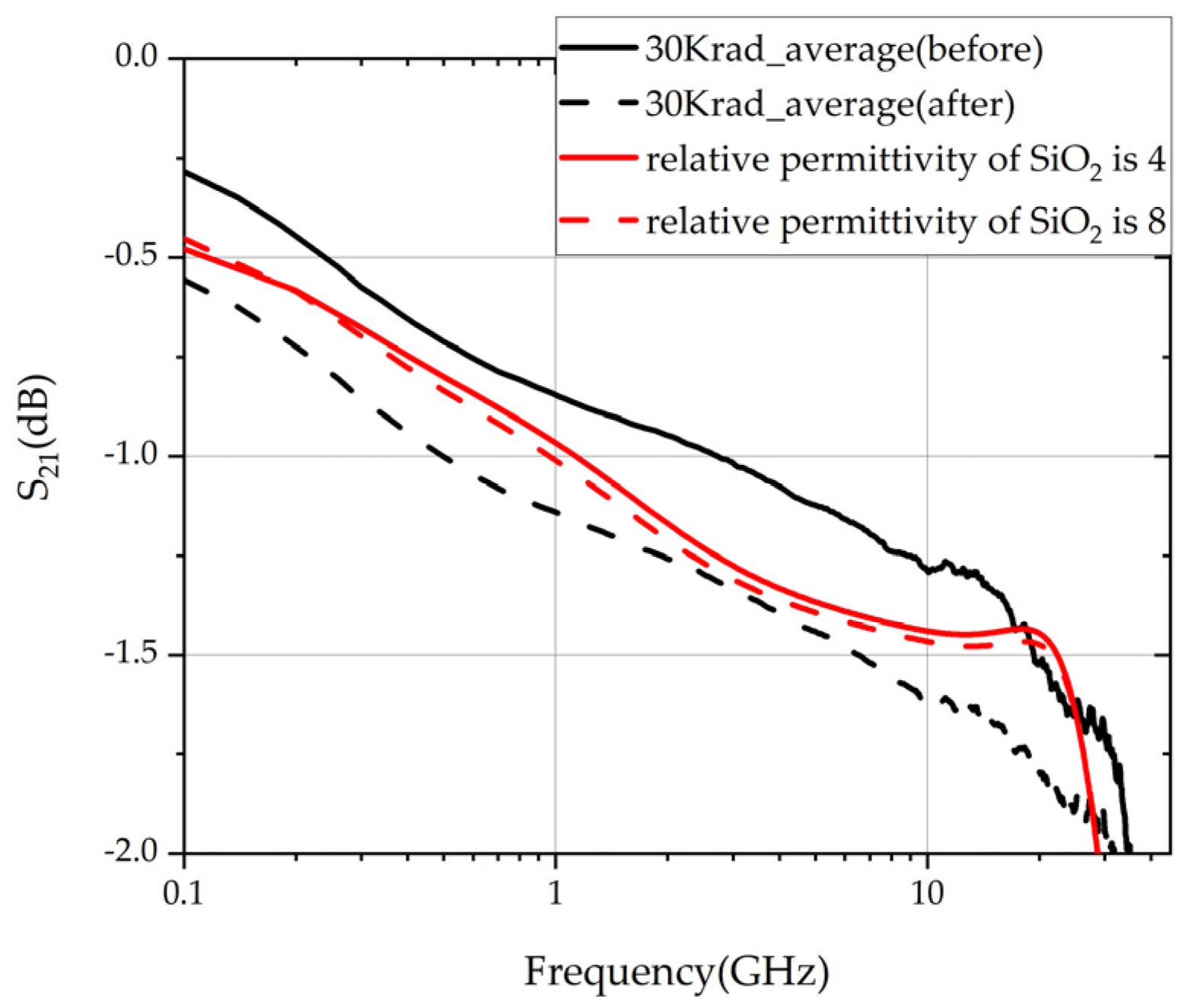
Figure 11 shows the S21 of the type A TSV component measured before and after the irradiation experiment, with the irradiation dose of 30 krad (Si), and the S21 of the type A model simulated in HFSS software, with the relative permittivity of SiO2 of 4 and 8.
As shown in Figure 11, within 40 GHz, the range of S21 of TSV components is above −2 dB, a relatively small value. According to the analysis in Section 2, the effect of increasing irradiation dose on SiO2 reflected the increasing relative permittivity of SiO2. Though irradiation would cause the deterioration of S21 of TSV components, the rising irradiation dose does not mean the linear change in S21, as shown in Figure 8. In the simulation in HFSS software, the deterioration of S21 caused by the shift of relative permittivity of SiO2 was nonlinear, and the variation trend was consistent with the previous analysis based on experimental results. The S21 of TSV components degraded because of irradiation, further reflecting the degradation of the performance of TSV capacitance.
6. Conclusions
RF systems utilizing 3D integration technology have been widely used, while the TID effect on TSVs has been neglected, hindering its application in space and in the nuclear industry. The simulation results based on a 1D model of the TSV structure showed that after irradiation, the greater the irradiation dose, the more the CV curves of the TSV capacitance drifted to the left. It was necessary to set the working point of the TSV capacitor in the accumulation zone, and to leave a certain margin for the left drift of the irradiated CV curve, to ensure the stability of the TSV capacitor. Then, three types of TSV components were designed and manufactured, and the irradiation experiment based on them was conducted. The variation trend of the S21 of the model in HFSS was consistent with the experimental data, and it can be concluded that the effect of irradiation on the TSV component was nonlinear. With the increasing irradiation dose, the S21 of the TSV components deteriorated, while the variation of S21 decreased. Experimenting with a large number of TSV components, and performing statistical analysis, helped to eliminate errors. In the case of insufficient data, the error was reduced by taking the average. Though the error still interfered with further quantitative analysis, the qualitative research was still very persuasive. The simulation and irradiation experiment validated a relatively accurate method for assessing the RF systems’ performance under an irradiation environment, and the TID effect on structures similar to TSV in RF systems, such as through-silicon capacitors.
Author Contributions
Conceptualization, L.Y. and Y.F.; methodology, G.S. and L.Y.; software, Z.L. and L.Y.; validation, L.Y., Y.F. and Q.L.; formal analysis, L.Y. and Q.L.; investigation, L.Y.; data curation, Z.L.; writing—original draft preparation, Z.L. and L.Y.; writing—review and editing, L.Y. and Z.L.; visualization, Z.L.; supervision, G.S.; project administration, L.Y.; funding acquisition, G.S. All authors have read and agreed to the published version of the manuscript.
Funding
This work was funded in part by the National Natural Science Foundation of China (NSFC), Grant Number 62074121, and in part by the National High Technology Research and Development Program of China (No. 2019YFB2204402).
Data Availability Statement
The data presented in this study are available on request from the corresponding author. The data are not publicly available due to the regulations of the research institutions.
Acknowledgments
Guoliang Li gave constructive suggestions during the article’s writing.
Conflicts of Interest
The authors declare no conflict of interest.
References
- Jagannathan, S.; Loveless, T.D.; Zhang, E.X.; Fleetwood, D.M.; Schrimpf, R.D.; Haeffner, T.D.; Kauppila, J.S.; Mahatme, N.; Bhuva, B.L.; Alles, M.L.; et al. Sensitivity of High-Frequency RF Circuits to Total Ionizing Dose Degradation. IEEE Trans. Nucl. Sci. 2013, 60, 4498–4504. [Google Scholar] [CrossRef]
- Peng, C.; Hu, Z.; Ning, B.; Huang, H.; Zhang, Z.; Bi, D.; En, Y.; Zou, S. Total-Ionizing-Dose Induced Coupling Effect in the 130-nm PDSOI I/O nMOSFETs. IEEE Electron Device Lett. 2014, 35, 503–505. [Google Scholar] [CrossRef]
- Jazaeri, F.; Zhang, C.M.; Pezzotta, A.; Enz, C. Charge-Based Modeling of Radiation Damage in Symmetric Double-Gate MOSFETs. IEEE J. Electron Devices Soc. 2017, 6, 85–94. [Google Scholar] [CrossRef]
- Lee, M.; Cho, S.; Lee, N.; Kim, J. Design for High Reliability of CMOS IC with Tolerance on Total Ionizing Dose Effect. IEEE Trans. Device Mater. Reliab. 2020, 20, 459–467. [Google Scholar] [CrossRef]
- Feng, J.; Li, Y.D.; Fu, J.; Wen, L.; He, C.F.; Guo, Q. Effect of Total Ionizing Dose Damage on 8-Transistor CMOS Star Sensor Performance. Semiconductors 2021, 55, 108–115. [Google Scholar] [CrossRef]
- Budroweit, J.; Jaksch, M.; Borghello, G. Ultra-High Total Ionizing Dose Effects in a Highly Integrated and RF-Agile Transceiver. In Proceedings of the 2020 IEEE Radiation Effects Data Workshop (in Conjunction with 2020 NSREC), Santa Fe, NM, USA, 29 November–30 December 2020; pp. 1–4. [Google Scholar] [CrossRef]
- Li, Z.; Elash, C.J.; Jin, C.; Chen, L.; Xing, J.; Yang, Z.; Shi, S. Comparison of Total Ionizing Dose Effects in 22-nm and 28-nm FD SOI Technologies. Electronics 2022, 11, 1757. [Google Scholar] [CrossRef]
- Faccio, F.; Michelis, S.; Cornale, D.; Paccagnella, A.; Gerardin, S. Radiation-induced short channel (RISCE) and narrow channel (RINCE) effects in 65 and 133 nm MOSFETs. IEEE Trans. Nucl. Sci. 2015, 62, 32663–33270. [Google Scholar] [CrossRef]
- Zhang, C.M.; Jazaeri, F.; Pezzotta, A.; Bruschini, C.; Borghello, G.; Faccio, F.; Mattiazzo, S.; Baschirotto, A.; Enz, C. Characterization of GigaRad Total Ionizing Dose and Annealing Effects on 28-nm Bulk MOSFETs. IEEE Trans. Nucl. Sci. 2017, 64, 2639–2647. [Google Scholar] [CrossRef]
- Ma, T.; Bonaldo, S.; Mattiazzo, S.; Baschirotto, A.; Enz, C.; Paccagnella, A.; Gerardin, S. TID degradation mechanisms in 16 nm bulk FinFETs irradiated to ultra-high doses. IEEE Trans. Nucl. Sci. 2021, 68, 1571–1578. [Google Scholar] [CrossRef]
- Bonaldo, S.; Gorchichko, M.; Zhang, E.X.; Ma, T.; Mattiazzo, S.; Bagatin, M.; Paccagnella, A.; Gerardin, S.; Schrimpf, R.D.; Reed, R.A.; et al. TID effects in highly scaled gate-all-around Si nanowire CMOS transistors irradiated to ultra-high doses. IEEE Trans. Nucl. Sci. 2022, 69, 1444–1452. [Google Scholar] [CrossRef]
- Simoen, E.; Gaillardin, M.; Paillet, P.; Reed, R.A.; Schrimpf, R.D.; Alles, M.L.; El-Mamouni, F.; Fleetwood, D.M.; Griffoni, A.; Claeys, C. Radiation Effects in Advanced Multiple Gate and Silicon-on-Insulator Transistors. IEEE Trans. Nucl. Sci. 2013, 60, 1970–1991. [Google Scholar] [CrossRef]
- Fleetwood, D.M. Radiation Effects in a Post-Moore World. IEEE Trans. Nucl. Sci. 2021, 68, 509–545. [Google Scholar] [CrossRef]
- Yanruoyue, L.; Guicui, F.; Xiaojun, Y.; Weifang, Z. Thermodynamic Analysis of SiO2 Thickness’s Effect on TSV. In Proceedings of the 2018 19th International Conference on Thermal, Mechanical and Multi-Physics Simulation and Experiments in Microelectronics and Microsystems (EuroSimE), Toulouse, France, 15–18 April 2018. [Google Scholar]
- Li, K.; Zhang, E.X.; Gorchichko, M.; Wang, P.F.; Reaz, M.; Zhao, S.E.; Hiblot, G.; Van Huylenbroeck, S.; Jourdain, A.; Alles, M.L.; et al. Impacts of Through-Silicon Vias on Total-Ionizing-Dose Effects and Low-Frequency Noise in FinFETs. IEEE Trans. Nucl. Sci. 2021, 68, 740–747. [Google Scholar] [CrossRef]
- Liu, Z.; Swarup, S.; Tan, S.X.D. Compact Lateral Thermal Resistance Modeling and Characterization for TSV and TSV Array. In Proceedings of the 2013 IEEE/ACM International Conference on Computer-Aided Design (ICCAD), San Jose, CA, USA, 18–21 November 2013. [Google Scholar]
- Chen, G.; Wang, Z.; Wang, W. Influence of Different Materials on Thermal Stress of Conical TSV. In Proceedings of the 2018 19th International Conference on Electronic Packaging Technology (ICEPT), Shanghai, China, 8–11 August 2018. [Google Scholar]
- Shan, G.; Lu, Q.; Liu, S.; Yang, Y. Through-Silicon Capacitor Interconnection for High Frequency 3-D Microsystem. IEEE Trans. Compon. Packag. Manuf. Technol. 2019, 9, 1310–1318. [Google Scholar] [CrossRef]
- Yang, L.H.; Li, Z.M.; Fu, Y.; Li, G.L.; Lu, Q.J. Study of Total Ionizing Dose on RF Microsystem. In Proceedings of the 4th International Conference on Microelectronic Devices and Technologies (MicDAT ’2022), Corfu, Greece, 21–23 September 2022. [Google Scholar]
- COMSOL AB. Interface Trapping Effects of a MOSCAP, COMSOL Multiphysics® v. 5.4; COMSOL AB: Stockholm, Sweden, 2018; pp. 2–22. [Google Scholar]
- Cendes, Z. The development of HFSS. In Proceedings of the 2016 USNC-URSI Radio Science Meeting, Fajardo, PR, USA, 26 June–1 July 2016. [Google Scholar] [CrossRef]
- Paillet, P.; Touron, J.L.; Leray, J.L.; Cirba, C.; Michez, A. Simulation Of Multi-Level Radiation-Induced Charge Trapping and Thermally Activated Phenomena in SiO2. IEEE Trans. Nucl. Sci. 1998, 45, 1379–1384. [Google Scholar] [CrossRef]
Figure 1.
TSV architecture: (a) longitudinal section, (b) cross-section.
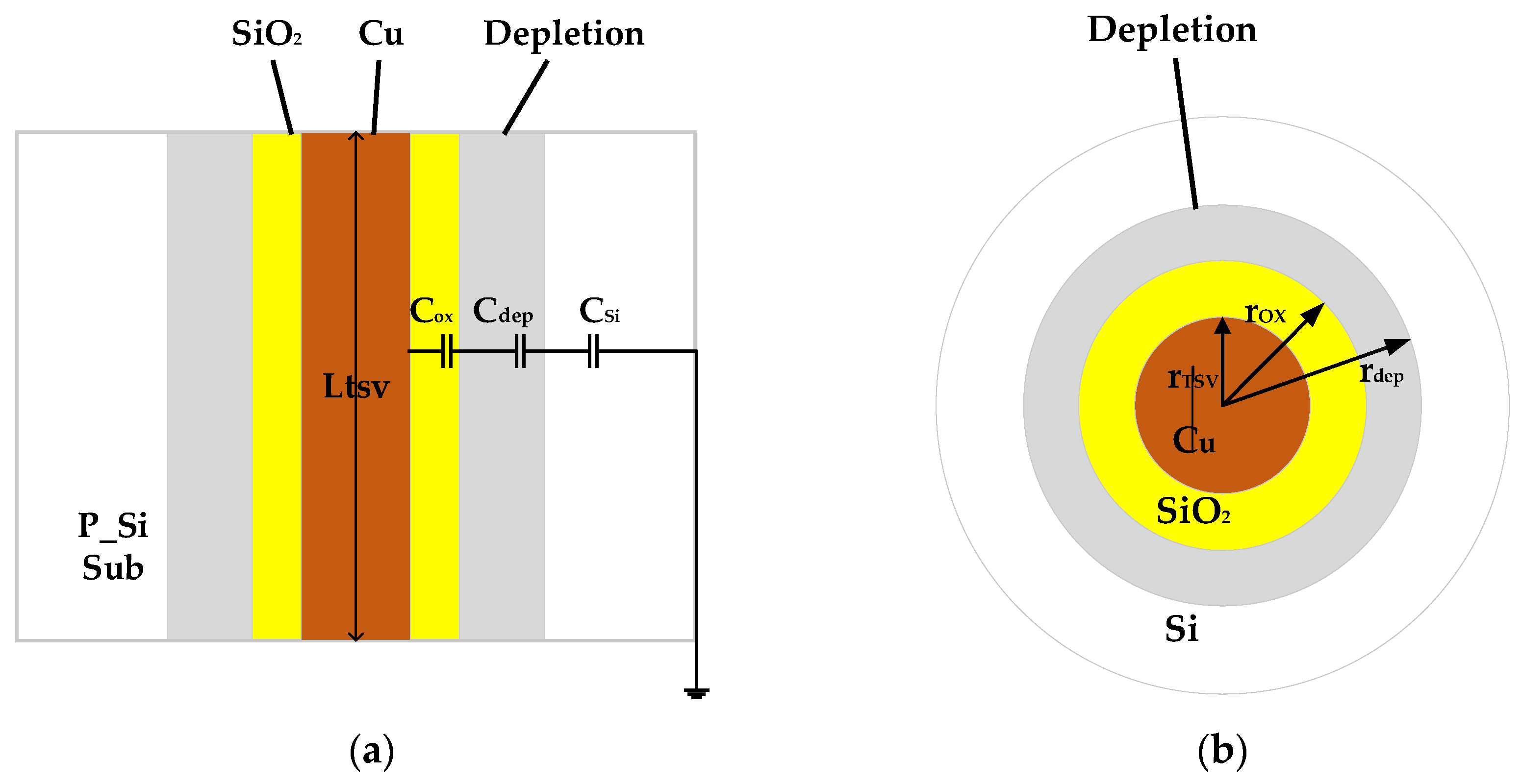
Figure 2.
1D modeling of TSV (the p-type) in COMSOL.
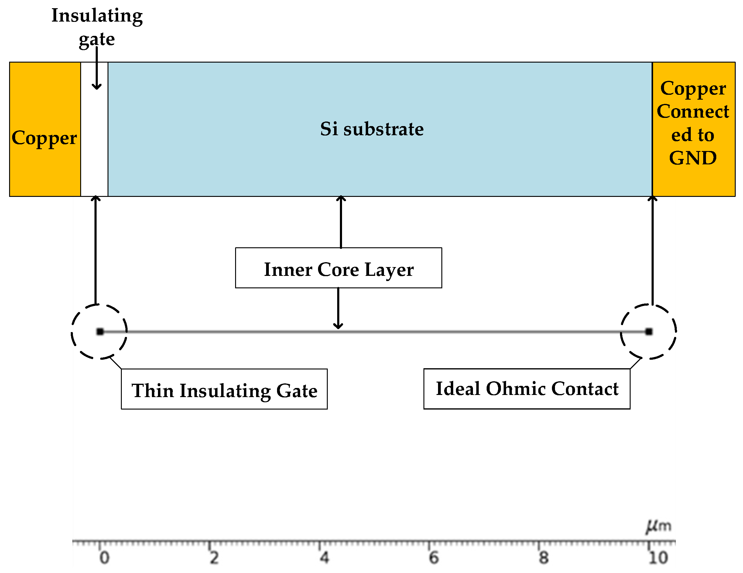
Figure 3.
CV curve of TSV capacitance after irradiation. (a) low frequencies; (b) high frequencies.
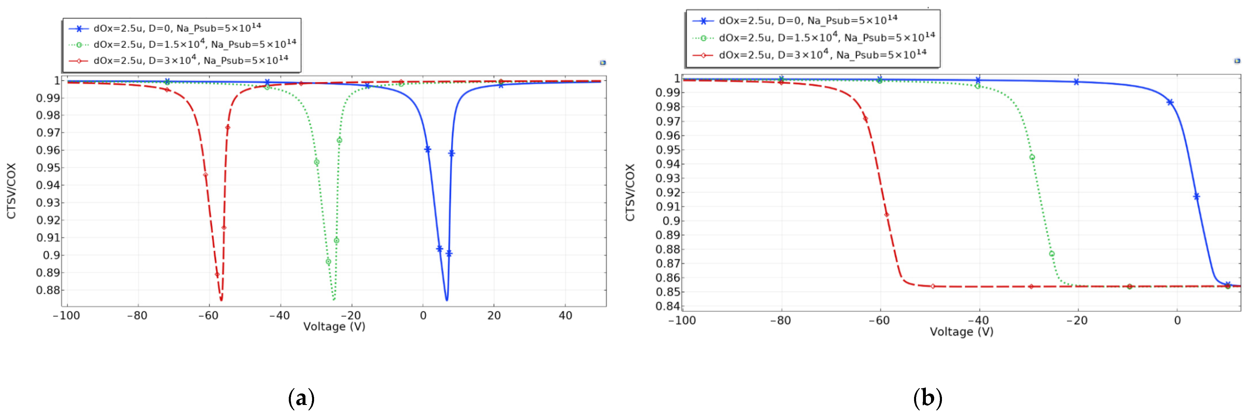
Figure 4.
CV curves of irradiated TSV capacitances with different oxide thicknesses: (a) low frequencies, (b) high frequencies.
Figure 4.
CV curves of irradiated TSV capacitances with different oxide thicknesses: (a) low frequencies, (b) high frequencies.
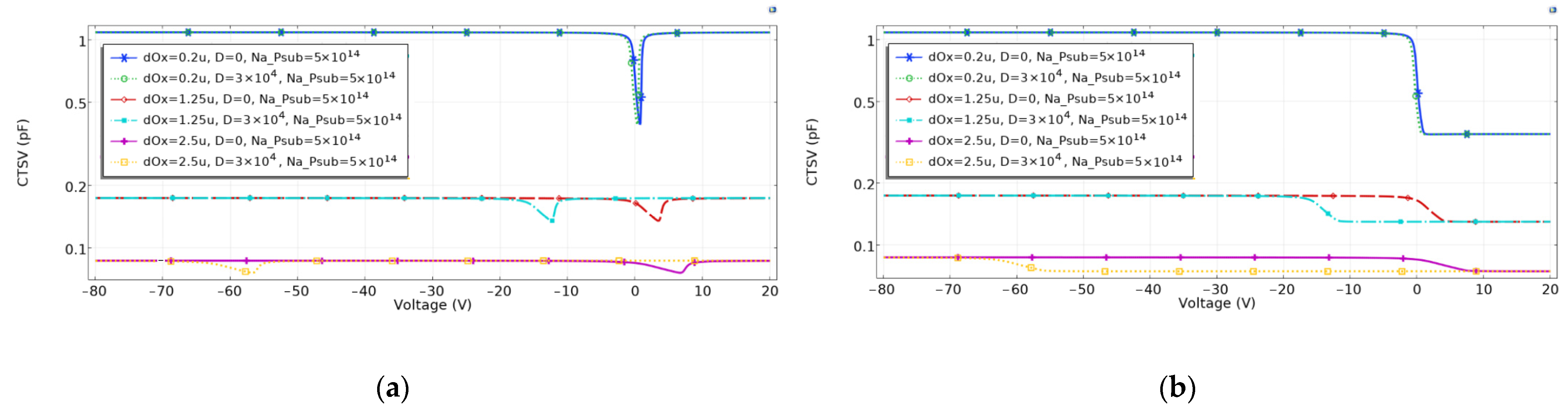
Figure 5.
CV curve of irradiated TSV capacitances with substrate doping concentration at (a) low frequencies, and (b) high frequencies.
Figure 5.
CV curve of irradiated TSV capacitances with substrate doping concentration at (a) low frequencies, and (b) high frequencies.
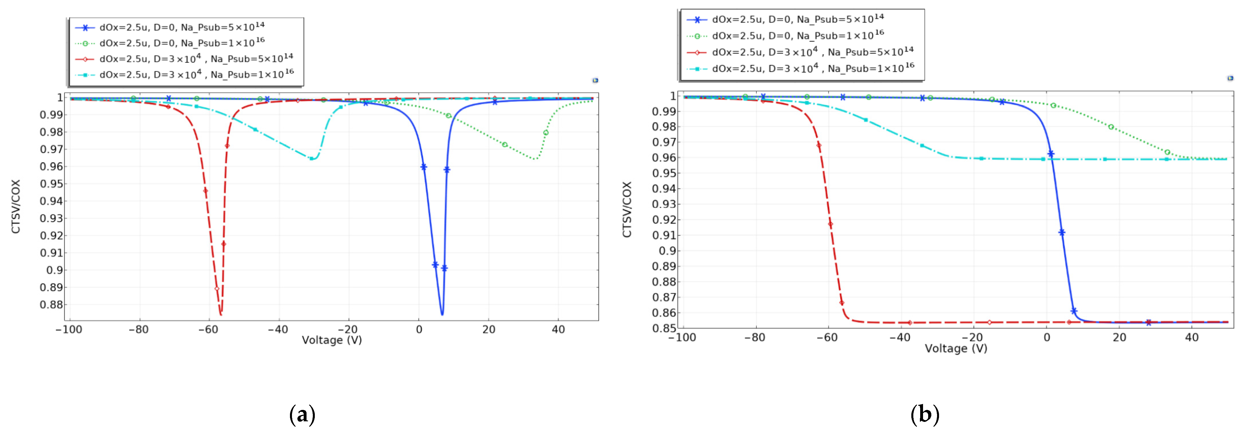
Figure 6.
Three types of TSV components: (a) type A, (b) type B, and (c) type C.

Figure 7.
(a) The testing environment of the TSV components. (b) Probes and TSV components.

Figure 8.
Average S21 variation of three types of TSV components before and after irradiation experiment: (a) type A, (b) type B, (c) type C.
Figure 8.
Average S21 variation of three types of TSV components before and after irradiation experiment: (a) type A, (b) type B, (c) type C.
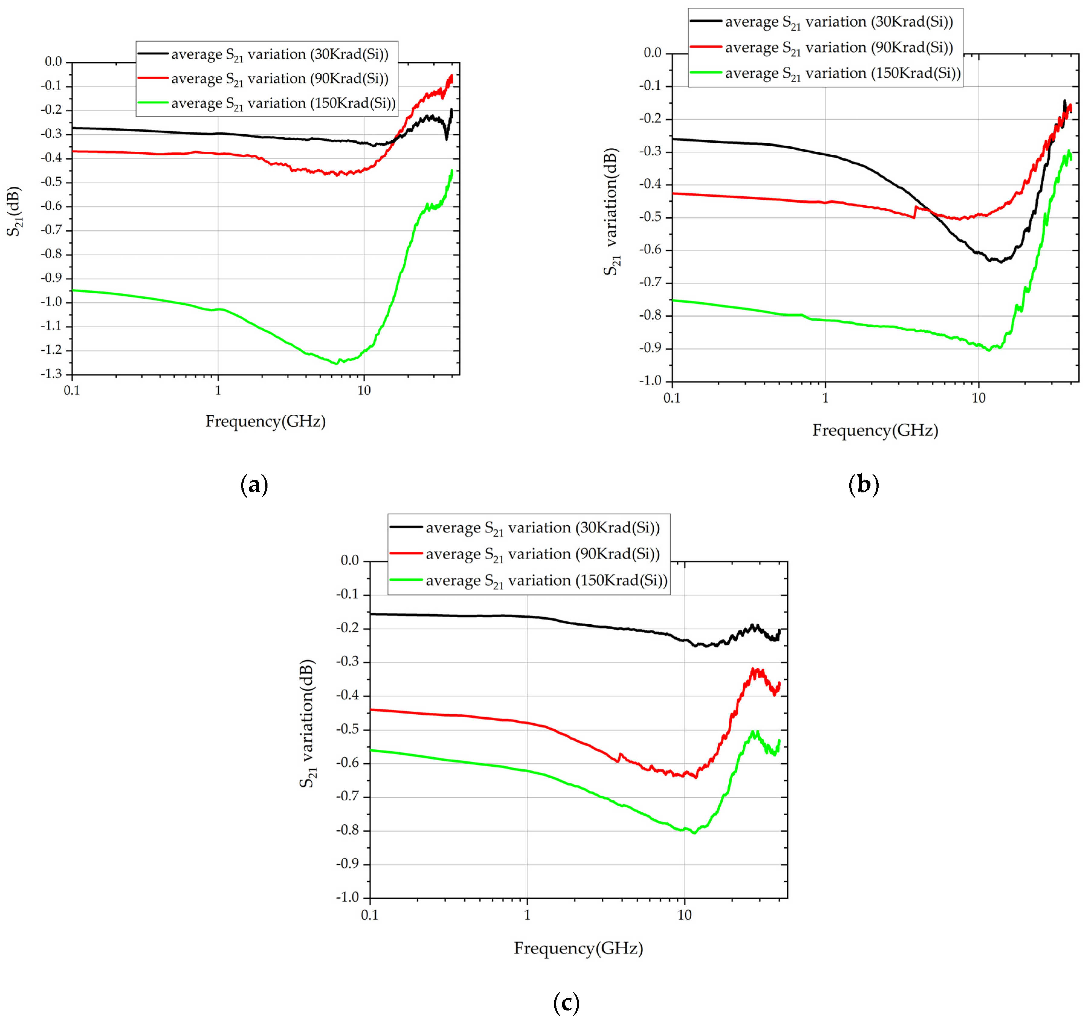
Figure 9.
TSV model of type A modeled in HFSS: (a) flat view of the TSV model; (b) top view of the TSV model.
Figure 9.
TSV model of type A modeled in HFSS: (a) flat view of the TSV model; (b) top view of the TSV model.
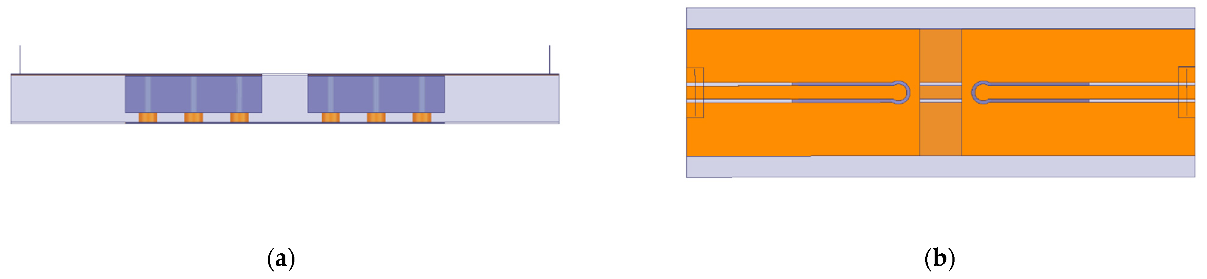
Figure 10.
S21 simulated in HFSS, based on the TSV model of type A.

Figure 11.
S21 of TSV component of type A.


Table 1.
Experimental conditions of different irradiation doses.
| Irradiation Dose | Experimental Conditions | |
|---|---|---|
| Irradiation Rate (rad/s) | Irradiation Time (min) | |
| 30 krad (Si) | 50 | 10 |
| 90 krad (Si) | 50 | 30 |
| 150 krad (Si) | 50 | 50 |
Table 2.
Variation of S21 at different frequencies, and at different relative permittivities of SiO2.
Table 2.
Variation of S21 at different frequencies, and at different relative permittivities of SiO2.
| The Relative Permittivity of SiO2 | 1 GHz | 5 GHz | 10 GHz | 15 GHz | 20 GHz |
|---|---|---|---|---|---|
| 4 | −0.96656 | −1.36706 | −1.43972 | −1.44308 | −1.44511 |
| 8 | −0.04377 | −0.02657 | −0.02608 | −0.03188 | −0.02888 |
| 12 | −0.06195 | −0.03464 | −0.03526 | −0.046 | −0.04344 |
| 16 | −0.06711 | −0.03547 | −0.03693 | −0.05096 | −0.04852 |
| 20 | −0.08022 | −0.03451 | −0.03634 | −0.05446 | −0.05253 |
Disclaimer/Publisher’s Note: The statements, opinions and data contained in all publications are solely those of the individual author(s) and contributor(s) and not of MDPI and/or the editor(s). MDPI and/or the editor(s) disclaim responsibility for any injury to people or property resulting from any ideas, methods, instructions or products referred to in the content. |
© 2023 by the authors. Licensee MDPI, Basel, Switzerland. This article is an open access article distributed under the terms and conditions of the Creative Commons Attribution (CC BY) license (https://creativecommons.org/licenses/by/4.0/).
Share and Cite
MDPI and ACS Style
Yang, L.; Li, Z.; Shan, G.; Lu, Q.; Fu, Y. Modeling and Validation of Total Ionizing Dose Effect on the TSVs in RF Microsystem. Micromachines 2023, 14, 1180. https://doi.org/10.3390/mi14061180
AMA Style
Yang L, Li Z, Shan G, Lu Q, Fu Y. Modeling and Validation of Total Ionizing Dose Effect on the TSVs in RF Microsystem. Micromachines. 2023; 14(6):1180. https://doi.org/10.3390/mi14061180
Chicago/Turabian StyleYang, Lihong, Zhumeng Li, Guangbao Shan, Qijun Lu, and Yu Fu. 2023. "Modeling and Validation of Total Ionizing Dose Effect on the TSVs in RF Microsystem" Micromachines 14, no. 6: 1180. https://doi.org/10.3390/mi14061180
Note that from the first issue of 2016, this journal uses article numbers instead of page numbers. See further details here.