
A Ternary Inverter Based on Hybrid Conduction Mechanism of Band-to-Band Tunneling and Drift-Diffusion Process


1
School of Physics and Information Engineering, Shanxi Normal University, Taiyuan 030024, China
2
Shaanxi Province Key Laboratory of Thin Films Technology and Optical Test, Xi’an Technological University, Xi’an 710032, China
*
Author to whom correspondence should be addressed.
Micromachines 2024, 15(4), 522; https://doi.org/10.3390/mi15040522
Submission received: 10 March 2024
/
Revised: 9 April 2024
/
Accepted: 10 April 2024
/
Published: 13 April 2024
(This article belongs to the Special Issue Development and Application of Advanced Electronic Nanodevices)
Abstract
:In this paper, a novel transistor based on a hybrid conduction mechanism of band-to-band tunneling and drift-diffusion is proposed and investigated with the aid of TCAD tools. Besides the on and off states, the proposed device presents an additional intermediate state between the on and off states. Based on the tri-state behavior of the proposed TDFET (tunneling and drift-diffusion field-effect transistor), a ternary inverter is designed and its operation principle is studied in detail. It was found that this device achieves ternary logic with only two components, and its structure is simple. In addition, the influence of the supply voltage and the key device parameters are also investigated.
1. Introduction
In recent decades, driven by the pursuit of enhanced performance in binary logic chips and increased information density, the MOSFET (metal-oxide-semiconductor field-effect transistor) dimension has been rapidly reduced. However, the modulation of carrier thermionic emission over the energy barrier controlled by the gate bias poses challenges for MOSFETs in surpassing the sub-threshold swing (SS) limitation of 60 mV/dec at room temperature. This limitation leads to a rapid increase in the leakage current and power density during the miniaturization process [1,2,3,4]. Consequently, this presents a significant obstacle to further advancement in information density and circuit performance. Although steep slope devices, such as negative-capacitance FETs (NCFETs) [5,6,7,8,9] and tunneling FETs (TFETs) [10,11,12,13,14], can mitigate this issue, the number of bits is inherently smaller than the number of gates in a binary Boolean logic system [2].
Fundamentally, the most promising strategy for addressing the power challenge and significantly improving information density involves a shift from traditional binary logic to ternary logic [15,16,17,18,19]. In binary systems, information is represented by {0, 1}, whereas in a ternary system, it is represented by {0, 1, 2} or {−1, 0, 1}. Consequently, in a ternary system, the number of ternary bits can exceed the number of gates, a crucial factor for increasing the information density. With the same number of gates, ternary logic can accommodate more information, leading to higher information density. Alternatively, to store equivalent information, ternary logic has the potential to reduce the number of required devices, pins, and connections. Ultimately, this transition can drastically decrease the overall system complexity to 63.1% [1,4,20].
The advancement of the standard ternary inverter (STI) represents a crucial foundational element in the development of ternary logic systems. Its practical implementation holds immense significance and garners substantial attention within the field. Currently, two methods exist for realizing STIs. One approach involves the direct design of the STI using MOSFETs, initially preferred due to its compatibility with the CMOS platform. However, this method typically requires a larger number of MOSFETs for an STI, ranging from three to as many as five [21,22,23]. Additionally, it necessitates multiple power supplies, including additional voltages such as –VDD, 1/3VDD, and 2/3VDD [22,24], or passive elements like two additional resistors [25]. Consequently, this not only results in a larger chip area and increased power consumption, but also elevates the complexity of system design. As a result, recent years have witnessed a decline in research focused on STIs based on this approach.
An alternative approach involves constructing the STI using ternary devices that exhibit an intermediate state between the on and off states. Unlike the method mentioned earlier, this approach avoids an increase in the required device number and design complexity. However, the intermediate state, often arising from negative differential resistance (NDR) [26,27] and negative differential transconductance (NDT) [28,29], necessitates the use of heterojunctions formed by relatively novel and immature materials. Examples of such materials include BP/MoS2 [19,30], BP/ReS2/HfS2 [31], h-BN/WSe2/InSe [32], and even certain organic materials like PTCDI-C8 [33] and PTCDI-C13 [34]. Unfortunately, this reliance on novel materials renders this approach incompatible with the CMOS platform and poses challenges for mass producibility.
Obviously, based on the MOSFETs, the ternary logic inverter can be compatible with the CMOS technology, but it requires a passive component or multi-valued power supply, which makes the circuit significantly complex. The other method, with the aid of the ternary device, requires only two devices for implementing one ternary inverter and does not need multi-valued power supply, but this method relies on the novel immature materials that are incompatible with CMOS technology.
To address the issues and implement a ternary inverter compatible with the CMOS platform, a novel device combining the tunneling and drift-diffusion mechanisms is proposed. The proposed TDFETs can present three states without involving any novel immature material. Based on the TDFETs, a ternary inverter is designed and investigated. Additionally, the influences of the supply voltage as well as the key parameters of the TDFETs are studied in detail.
2. Device Structure and Simulation Setup
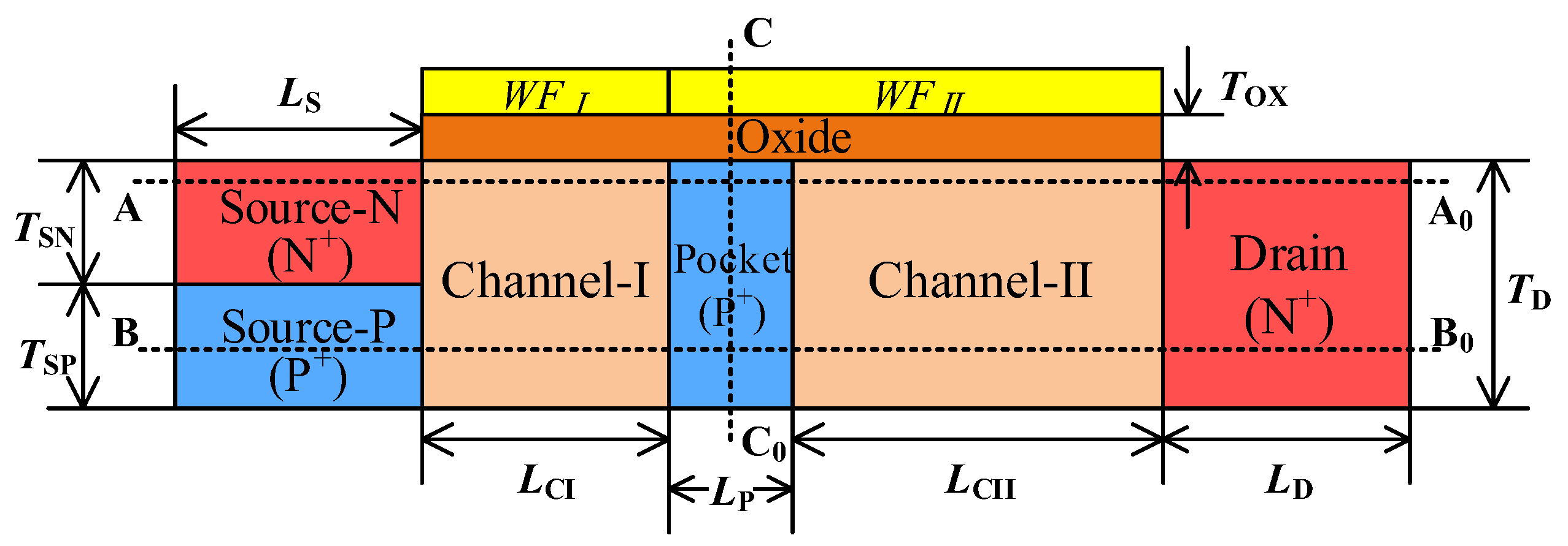
Figure 1 shows the device structure of the proposed TDFET. The source consists of two regions with the same concentration, but different doping types. The gate is divided into two parts, one with work function WFI and the other with work function WFII. The corresponding channels are channel-I and channel-II. A pocket is inserted into channel-II, enabling the device to conduct a current through different mechanisms. For the convenience of subsequent analysis and description, the cut-lines that would be used later are also marked in Figure 1. The cut lines AA0 and BB0 are 15 nm and 1 nm below the oxide/channel interface. The CC0 is perpendicular to the channel direction and located at the midpoint of the pocket region. The device parameters adopted in the simulation are listed in Table 1.
The proposed TDFET is studied using 2-D technology computer-aided technique (TCAD) tools(Sentaurus 2013). In order to account for the arbitrary tunneling barrier with a non-uniform electrical field, the BTBT model with a dynamic nonlocal path accounting for the arbitrary tunneling barrier with a non-uniform electrical field is adopted, and the nonlocal tunneling parameters [35,36] Apath and Bpath are 4 × 1014 cm−3·s−1 and 1.9 × 10⁷ V·cm−1, respectively. The Slotboom model is utilized to consider the influence of the high doping density on the band gap. Additionally, the doping-dependent mobility model, high-field velocity saturation model, and the Shockley–Read–Hall recombination models are also included.
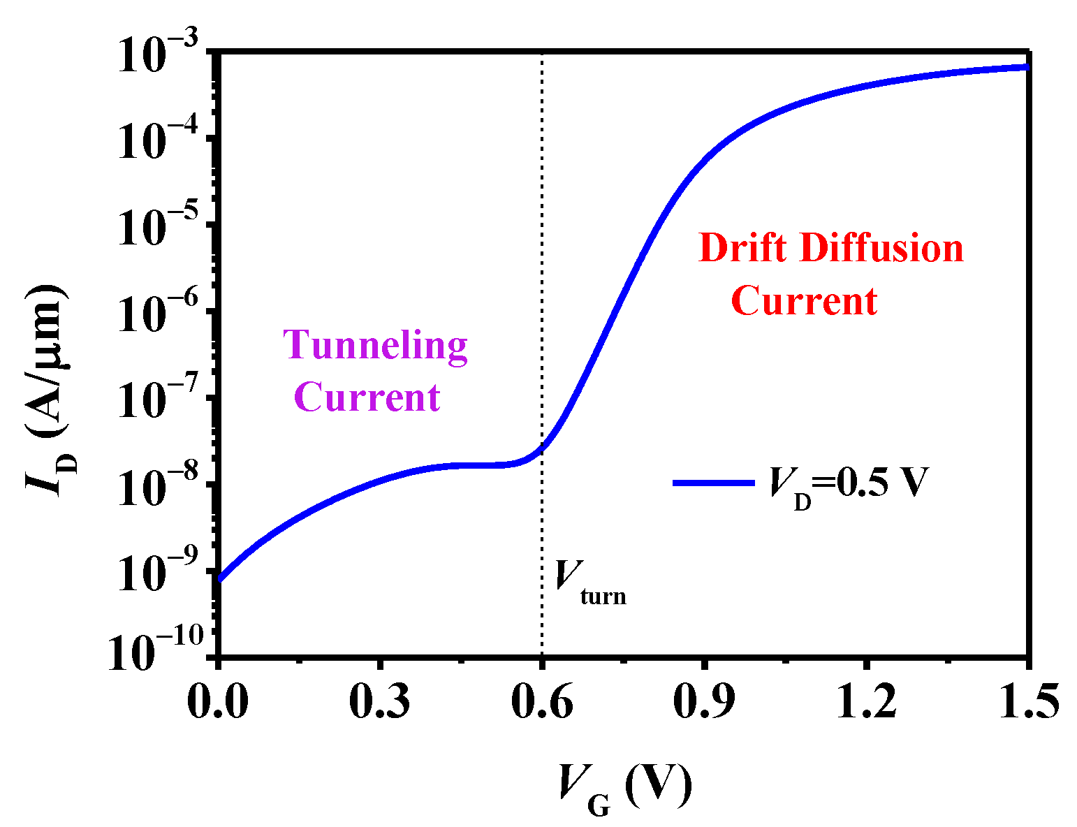
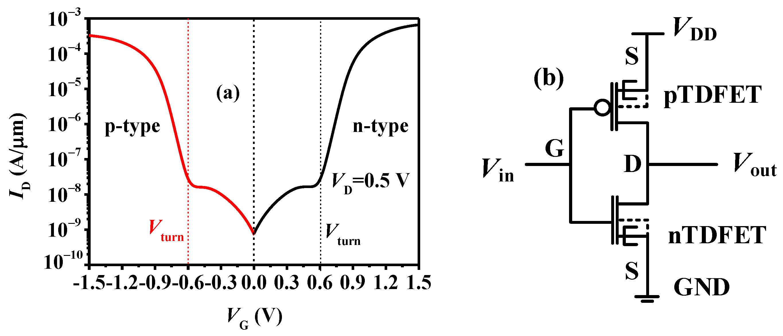
Figure 2 presents the transfer characteristics of the n-type TDFET. It is evident that the characteristics of the TDFET differ significantly from those of the conventional TFETs and MOSFETs. A noticeable transition occurs at a turn voltage (Vturn) of about 0.6 V, resulting in three distinct states in the TDFET, namely, the off-state, the on-state, and an intermediate state between the on and off states. This tri-state behavior of the TDFET makes it highly suitable for the design of ternary logic.
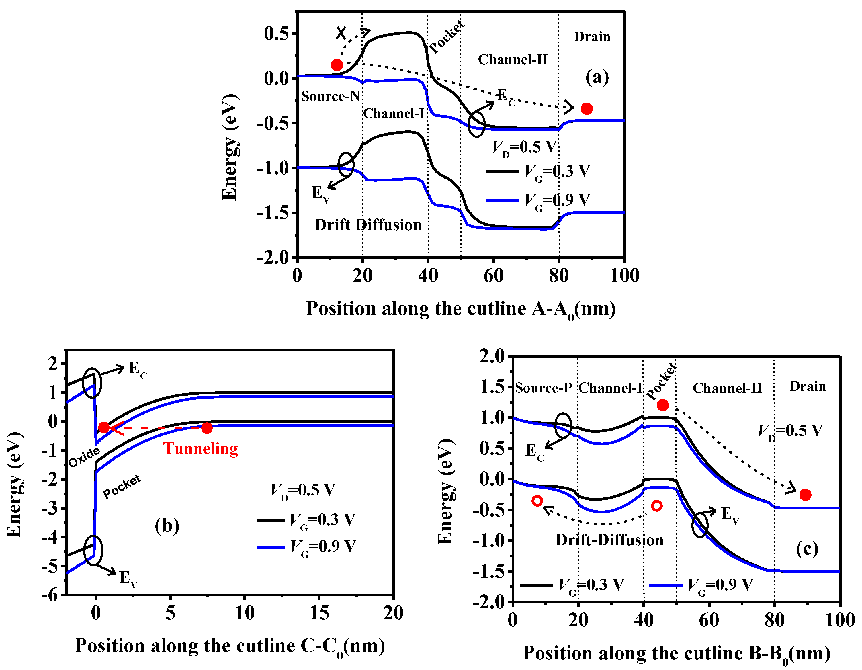
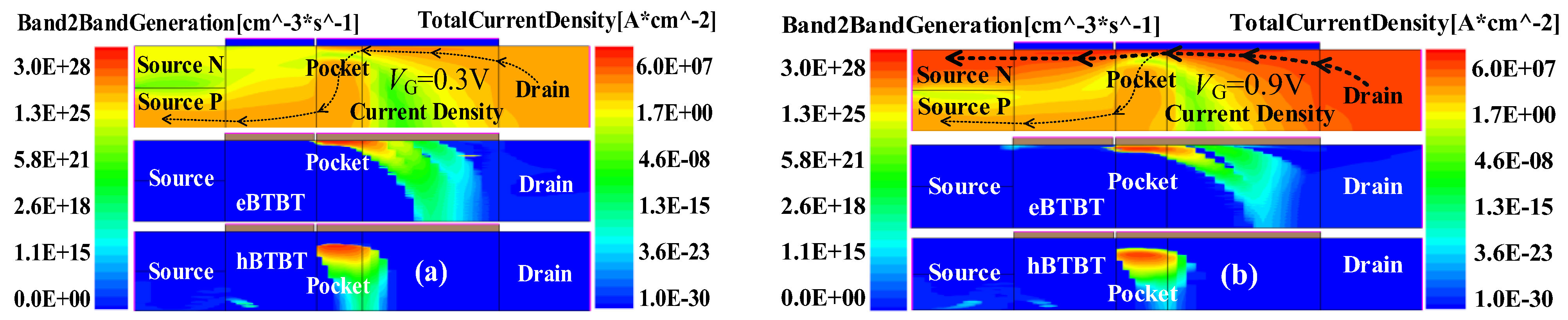
This tri-state behavior is actually caused by two different conduction mechanisms, as exhibited in Figure 3, showing the band diagrams along the cut-lines AA0, BB0, and CC0. Owing to the relatively large WFI, a high barrier of about 0.5 eV forms between the Source-N (SN) and channel-I regions at VG = 0.3 V, as presented in Figure 3a. This barrier blocks the electrons in the SN to the drain via the drift-diffusion mechanism. However, in this case, the conduction band (EC) in the pocket region near the oxide overlaps with the valance band (EV) further away, as depicted in Figure 3b. This allows the electrons farther away from the oxide to tunnel to the region near the oxide along the cut-line CC0, which can be verified in Figure 4a by the high electron band-to-band tunneling rate (eBTBT) near the oxide and high hole band-to-band tunneling rate (hBTBT) a little further away from the oxide in the pocket region. The tunneling electrons near the oxide drift further right along the channel to the drain, while the holes further away from the oxide drift left to the Source-P (SP), as shown in Figure 3c, forming the current path from the drain to the source along the dotted line with the arrow in the top figure of Figure 4a.
With the increased VG to 0.9 V, the EC in the channel-I descends. The barrier between the SN and the channel-I regions decreases, and even to zero, as shown in Figure 3a, allowing large amount of electrons in the SN region to be thermally injected into the channel-I and further drift to the drain. It should also be pointed out that the tunneling process in the pocket region still exists as shown in Figure 3b. Therefore, in this case, the tunneling and the drift-diffusing mechanisms coexist in the device. Figure 4b gives the distribution of the current density and tunneling rate at VG = 0.9 V. Obviously, there are high eBTBT and hBTBT in the pocket region. But there are many more electrons thermally injected from the SN than from the tunneling process. Thus, the drift-diffusion current is much higher than the tunneling current, and the current density is mainly distributed along the drift-diffusion current path indicated by the thicker dotted line in the top figure of Figure 4b.
Obviously, there are two conduction mechanisms in the TDFET. For VG < Vturn, the current is primarily dominated by the tunneling process in the pocket region and flows from the drain to the SP of the source. For VG > Vturn, the current is mainly governed by the drift-diffusion mechanism and flows from the drain to the SN of the source. As the drift-diffusion current is much greater than the tunneling current, a sudden increase in the current occurs near the Vturn and causes a noticeable transition on the transfer curve, forming the tri-state behavior of the proposed TDFET.
3. Ternary Inverter Based on the TDFET
To implement a ternary inverter, a p-type device with symmetrical characteristics to the n-type TDFET is designed. The structure of the p-type device is identical to that of the n-type device, except for the change in the doping type in all regions. The gate work functions WFI and WFII of the p-type device are adjusted as 4.47 and 5.64 eV, respectively. Additionally, the pocket concentration is set as 3.7 × 1019 cm−3. The other parameters remain the same as in Table 1. Figure 5a presents the obtained symmetrical n-type and p-type curves, which are desirable features for the inverter design. Figure 5b presents the circuit diagram of the ternary inverter, showing a simple connection where the gates of the n-type and p-type devices are connected as the input (Vin), and the drain is connected as the output (Vout), with the source of the p-type device connected to VDD (operating voltage of the inverter) and the source of the n-type device connected to GND, similarly to the binary inverter circuit.
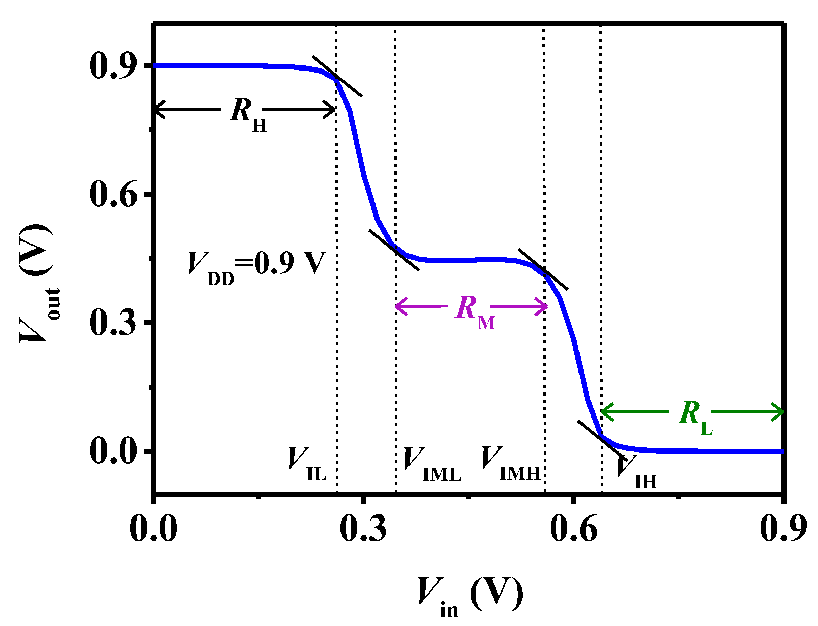
Figure 6 shows the voltage transfer characteristic (VTC) of the designed ternary inverter based on the TDFETs. It can be seen that the inverter exhibits three distinct output states. The VIL and VIH are the maximum and minimum of the input voltage and can be considered as the logic L and H, respectively. The VIML and VIMH are the minimum and maximum of the input voltage and can be considered as the logic M. The VIL, VIH, VIML, and VIMH are all defined at the points where the slope equals −1. The input voltage ranges corresponding to the logic L, M, and H are calculated as RL = VIL, RM = VIMH − VIML, and RH = VDD − VIH, respectively.
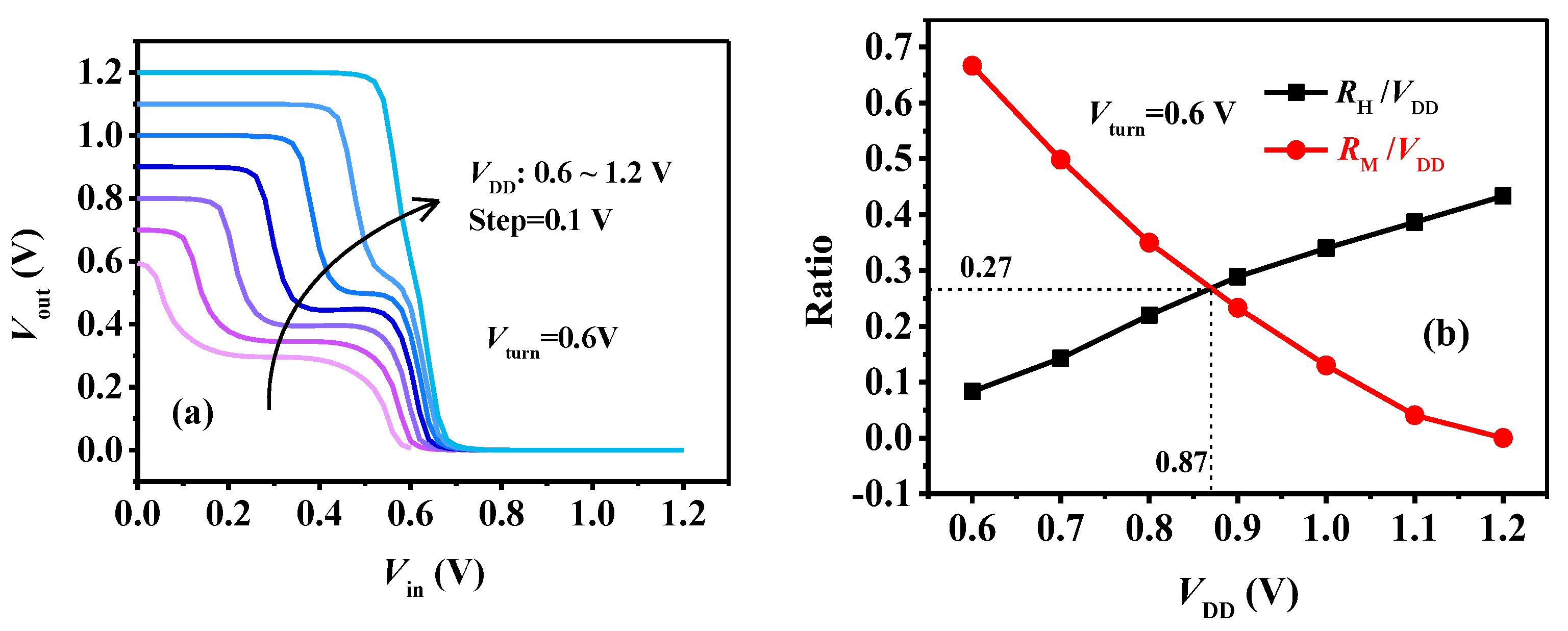
The VTC of the ternary inverter with various VDD from 0.6 V to 1.2 V is shown in Figure 7a. Interestingly, with increased VDD, the logic L and H show totally different changes compared to those of the intermediate logic M. The RM gradually decreases, while the RL and RH gradually increase with VDD. Even when VDD = 1.2 V, the intermediate logics M totally disappears and the ternary inverter becomes a conventional binary inverter. The varied RM and RH with VDD are extracted in Figure 7b. Due to the symmetrical transfer characteristics of the p-type and n-type devices, the RH ≈ RL (as can also be seen in Figure 7a), and therefore, RL/VDD is not present. We can see that as VDD increases, the RH/VDD gradually increases, while the RM/VDD decreases. When VDD = 1.45 Vturn = 0.87 V, RH ≈ RL = RM = 0.27 VDD, and the three levels are equiprobable, which is preferred for a ternary inverter.
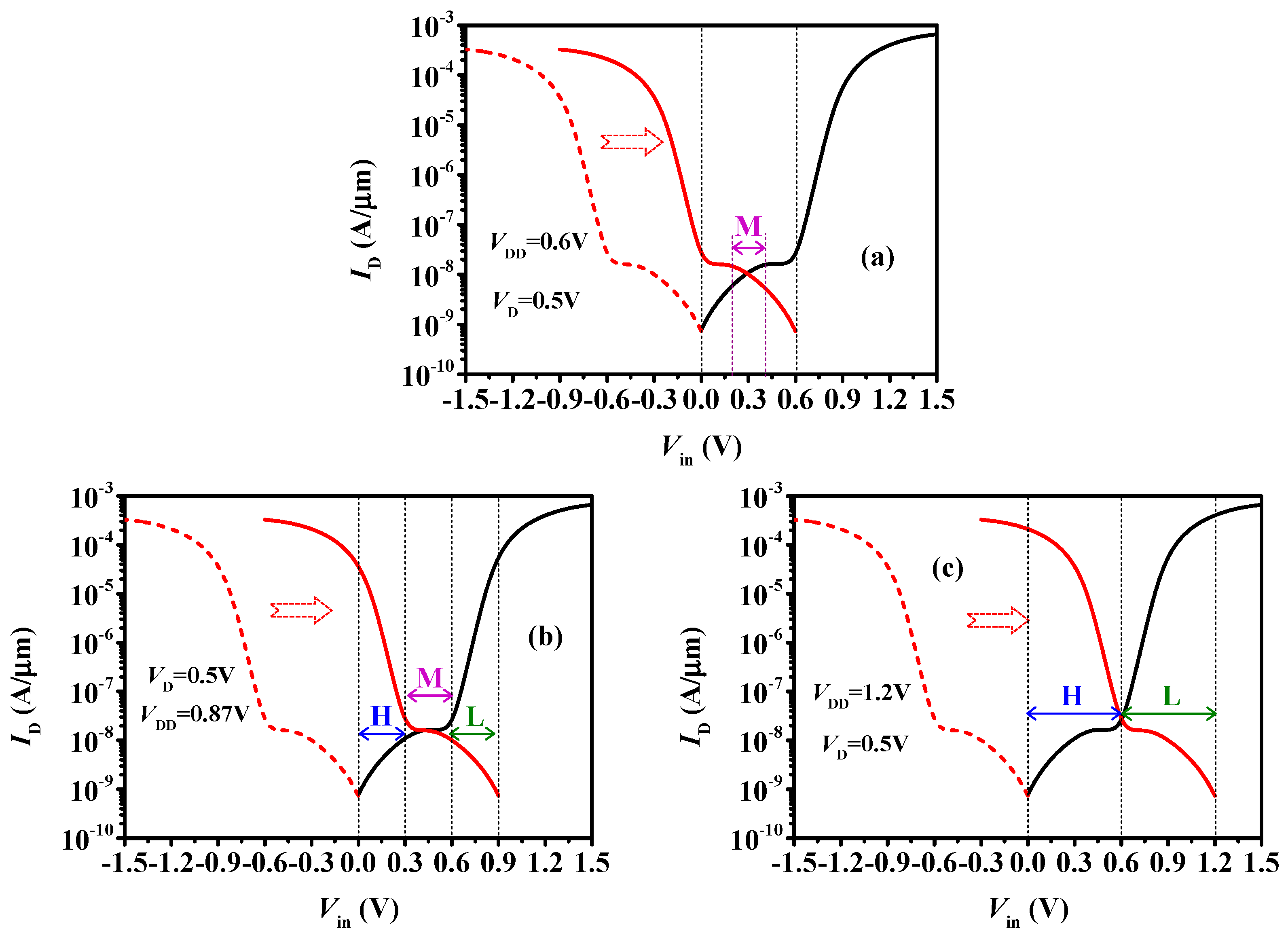
To further study the effects of VDD, the IDS varied with the input voltage Vin is plotted in Figure 8. Considering that in an inverter, the gate voltage of the n-type (VGn) and p-type TDFETs (VGp) are VGn = Vin and VGp = Vin − VDD, respectively, all we need is to shift the transfer curve of the p-type TDFET by VDD towards the positive direction to obtain the IDS-Vin characteristics. Figure 8a presents the IDS-Vin curves at VDD = 0.6 V. It can be seen that, as the Vin increases from 0.0 V to 0.2 V, the p-type device exhibits a larger current than the n-type device, and the resistance of the pull-up p-type device Rup is smaller than the pull-down n-type device Rdown, which results in Vout > VDD/2. Although the p-type current is larger than the n-type current, the maximum difference is less than an order of magnitude. This means the Rup is not small enough compared with the Rdown. Therefore, the logic H cannot be built, as shown in Figure 7a. The reason why the logic L disappears can be also explained in the similar way as the increase in Vin from 0.4 V to 0.6 V. For Vin increasing from 0.2 V to 0.4 V, both the devices operate in the transition region between the off state and the intermediate state, where the current and resistance of the devices are comparable. Thus, the output voltage is near 0.3 V (VDD/2). This is why the inverter only presents the logic M at a low voltage of VDD = 0.6 Vin (Figure 7a).
To make sure the inverter can present three distinct logics, the p-type transfer curve need to be shifted further to the right. That is to say that a larger VDD is required, as shown in Figure 8b, in which VDD = 0.9 V. It can be seen that when Vin is near 0V, the p-type TDFET is in the drift-diffusion region, while the n-type TDFET is in the off state. The Rup is much smaller than Rdown, and the high logic, H, forms. As for 0.3 V < Vin < 0.6 V, both the n-type and p-type devices operate in the tunneling current region in which the Rup ≈ Rdown and the Vout is near the VDD/2. Thus, the intermediate logic, M, is obtained. When Vin closes to the VDD, the p-type device enters the off-state while the n-type device enters the drift-diffusion region. Hence, the Rup is much larger than the Rdown, and the Vout approaches 0 V, resulting in the low logic L. This explains why the inverter can present three distinct levels at a VDD near 0.9 V.
However, as the VDD continues to increase, the input voltage range RM, over which both the n-type and p-type devices are in the tunneling current region, gradually decreases. The logic M on the VTC becomes more and more narrow. Until the VDD = 1.2 V, as shown in Figure 8c, the RM decreases to 0 and the intermediate logic M completely disappears. While the Vin rises from 0.0 V to VDD, there are only two distinct logics. Namely, when 0.0 V < Vin < VDD/2, the p-type current is far larger than the n-type current and the Rup < Rdown leading to logic H. When VDD/2 < Vin < VDD, the p-type current is far smaller than the n-type current and the Rup > Rdown, resulting in logic L. Obviously, in this case, the ternary inverter becomes a conventional binary inverter.
Based on the analysis presented in Figure 8, it is evident that VDD significantly influences the performance of the inverter. If we aim to design a ternary inverter with RL=RM=RH, we can deduce from Figure 8b that Vturn = (2/3)VDD, considering RL + RM + RH = VDD. In other words, the theoretical VDD for an ideal equiprobable ternary inverter is VDD = 1.5 Vturn. However, the practical scenario is that RL + RM + RH < VDD due to transitions between different logic states. This discrepancy is the reason why the equiprobable ratio RH/VDD = RM/VDD = 0.27 in Figure 7b is smaller than the ideal value of 1/3. Additionally, it explains why the VDD required for the equiprobable case is 0.87 V, slightly less than the theoretical value of 1.5 Vturn (0.9 V).
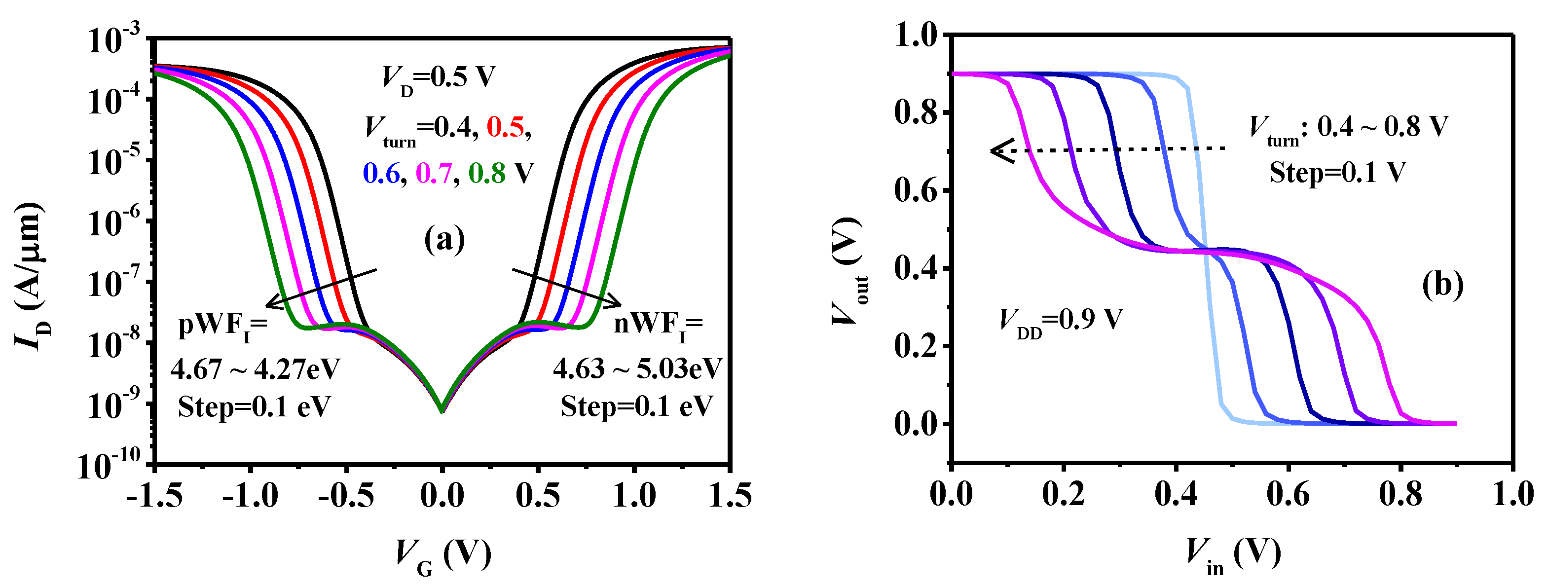
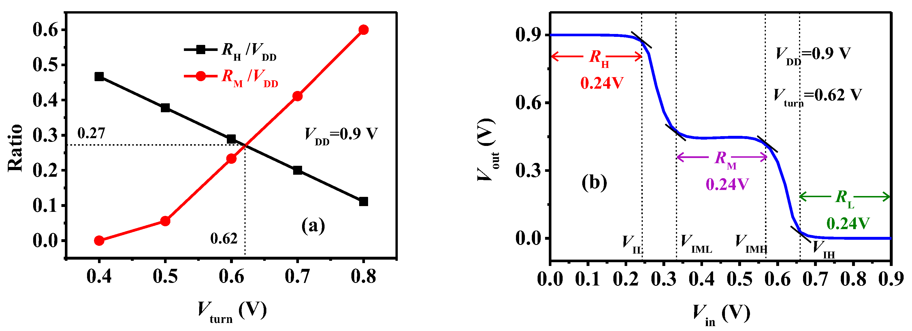
Obviously, we have the flexibility to adjust Vturn to achieve an equiprobable inverter for a specified VDD of 0.9 V. Considering that the Vturn is the critical gate voltage over which the drift-diffusion mechanism starts to dominate the device current, we can modulate the WFI to change the Vturn. Figure 9a depicts the symmetrical transfer curves of the TDFETs with different WFI. We can see that the absolute value of Vturn increases with the decreased WFI for the p-type TDFET and the increased WFI for the n-type device. As the absolute value of Vturn increases, the intermediate state of the transfer curve becomes flatter and more obvious. Thus, the input voltage range RM over which both the devices are in the intermediate state increases and the logic M gradually widens, as presented in Figure 9b, giving the variations in the VTC with Vturn at fixed VDD = 0.9 V. Figure 10a exhibits the varied RH/VDD and RM/VDD with Vturn, and we can see that, for VDD = 0.9 V, the ternary inverter becomes equiprobable at Vturn = 0.62 V. In this case, RH = RM ≈ 0.27 VDD. The corresponding VTC is plotted in Figure 10b. RM = RH = RL = 0.24 V indicates that the ternary inverter is equiprobable, and the subsequent simulations are based on this inverter.
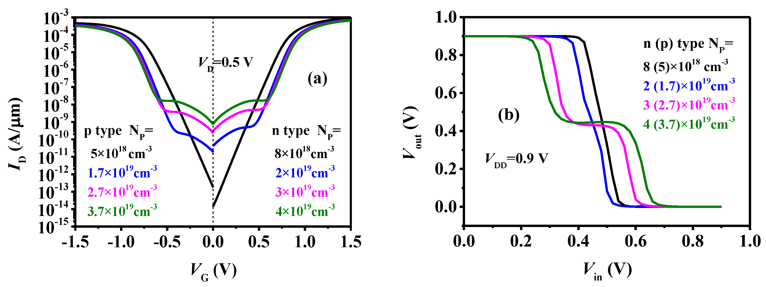
In a TDFET, the tunneling process happens in the pocket region. Thus, the pocket doping density NP and pocket length LP may show important effects. The symmetrical transfer curves of the n-type and p-type TDFETs with different NP are given in Figure 11a. It can be observed that, as the NP decreases, the tunneling-dominated current decreases, while the drift-diffusion-dominated current is hardly affected. This results in decreased Vturn and a weakened intermediate state between the on and off states, which further leads to gradually narrowing logic M on the VTC curve, as depicted in Figure 11b, which shows the varied VTC curves with NP. Until the NP decreases to 8 × 1018 cm−3 for the n-type device and 5 × 1018 cm−3 for the p-type device, the tunneling current, as well as the tri-state behavior, completely disappear, and the characteristics of the TDFET become almost identical to those of MOSFETs. In this case, the logic M on the VTC curve also completely disappears, and the ternary inverter becomes a conventional binary inverter.
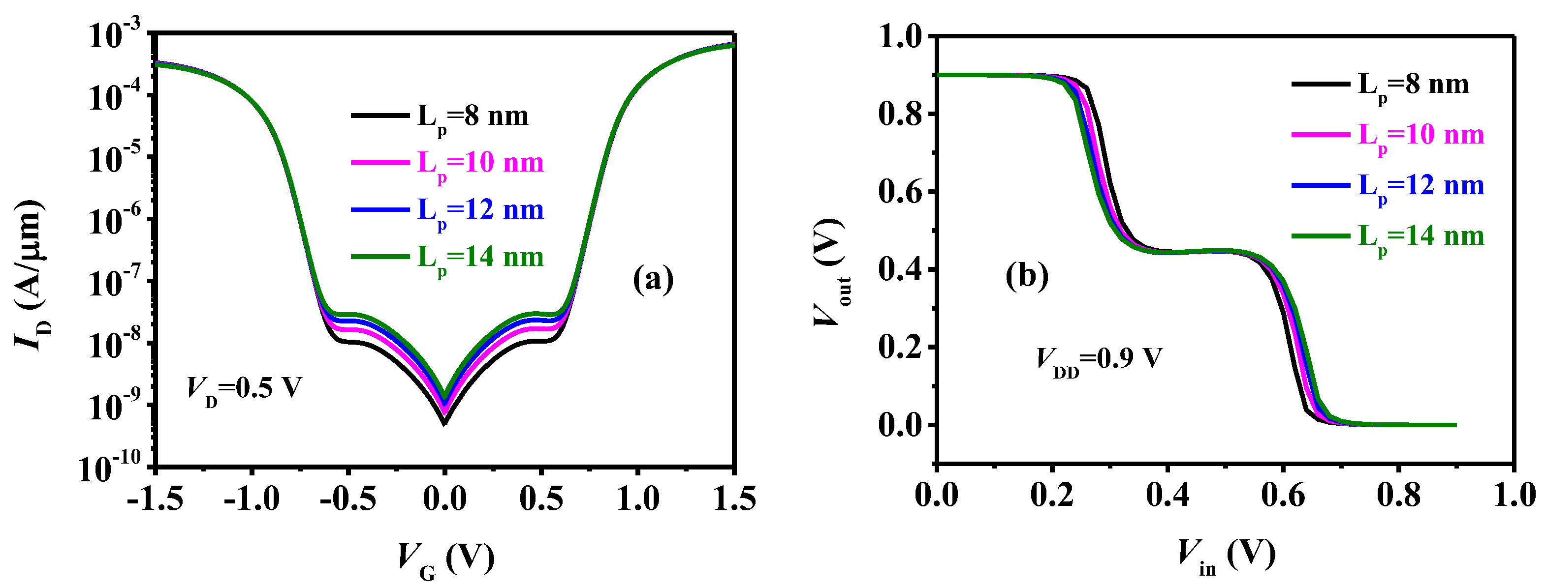
The influence of LP is illustrated in Figure 12. As LP increases, the effective tunneling area and the tunneling current gradually increase. However, the drift-diffusion current, primarily influenced by the barrier between the SN and channel-I regions, exhibits almost no variation. Consequently, this results in a slight increase in Vturn, as depicted in Figure 10a, and a subsequent slight widening of the logic M on the VTC, as shown in Figure 10b.
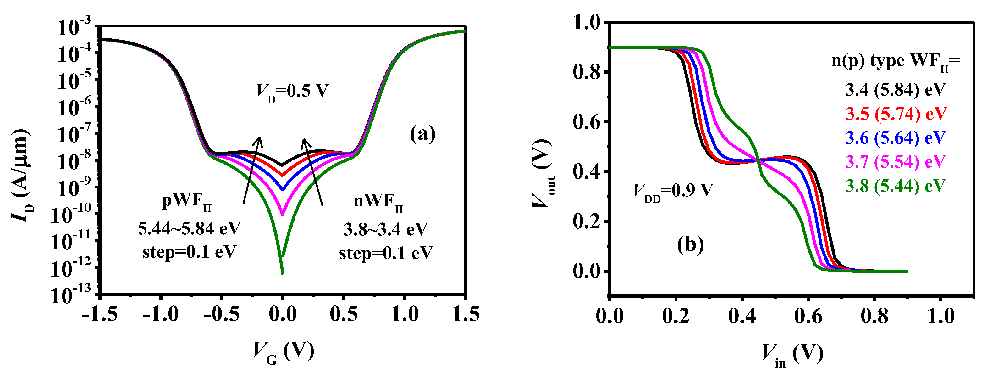
Figure 13 illustrates the impact of WFII. As the WFII increases for the p-type device and decreases for the n-type device, the tunneling current undergoes a gradual increase, resulting in a flatter intermediate state on the transfer curve, depicted in Figure 13a. Referencing the analysis in Figure 8, it becomes apparent that the flatter intermediate state contributes to a wider and flatter logic M, as shown in Figure 13b.
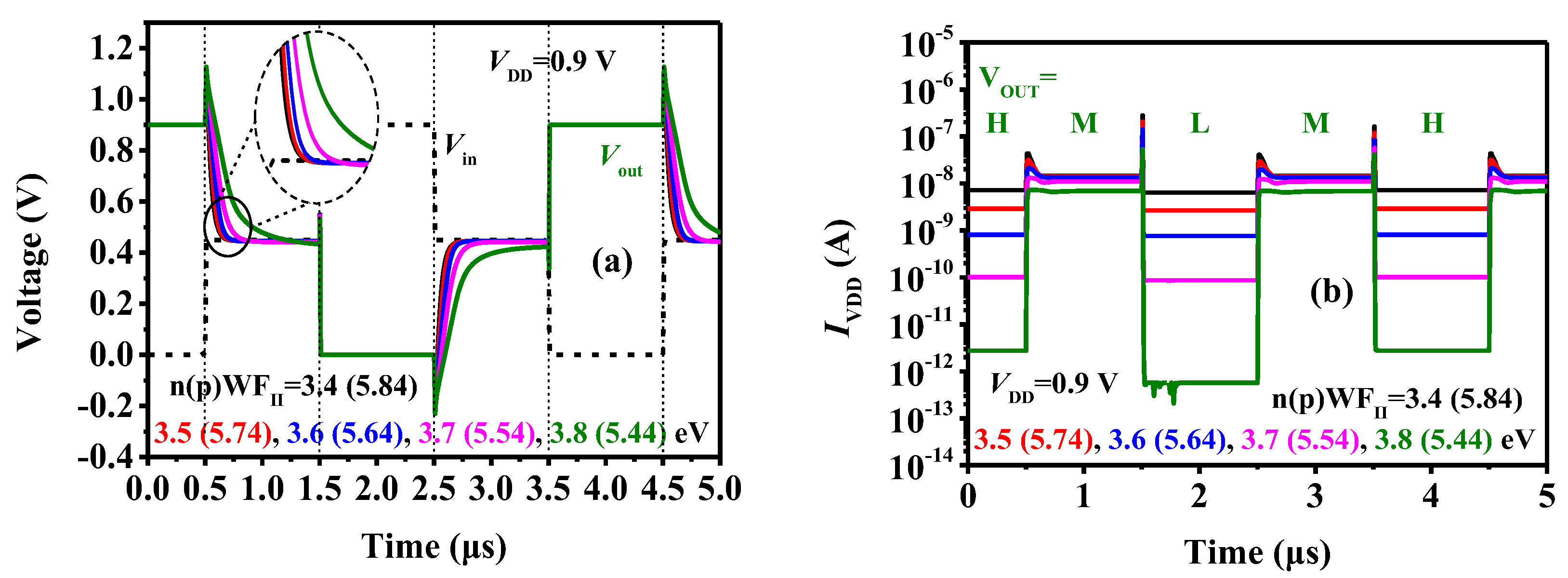
Figure 14a illustrates how WFII impacts the transient characteristics of the inverter. With changes in WFII, the tunneling current gradually decreases, leading to longer charging and discharging times for the capacitance. Consequently, the delay time for the inverter output to transition from level H to level M increases from 0.077 μs to 0.321 μs, causing a decrease in the inverter speed. Moreover, the variation in the intermediate state current affects the circuit power consumption. Figure 14b depicts the current variation from the power supply to the ground during the inverter output switching between different levels. It is evident that when the inverter outputs levels H and L, the power supply current is relatively small, whereas for level M, the power supply current is larger. This is attributed to the fact that at levels H and L, one of the n-type and p-type devices conducts while the other is turned off, resulting in no direct current path from the power supply to the ground. However, at level M, both n-type and p-type devices are in a partially conducting state, leading to the inverter power consumption being the sum of the n-type and p-type power consumption. Furthermore, as nWFII decreases and pWFII increases, both the intermediate state current and the off-state current of the device increase, resulting in a gradual increase in the inverter current. In conclusion, WFII significantly impacts the stability, speed, and power consumption of the inverter’s intermediate state. In practical design, inverters must balance stability, speed, and power consumption based on the circuit’s application scenarios.
4. Conclusions
In this paper, a novel TDEFT is proposed based on the band-to-band tunneling and drift-diffusion processes. Owing to the hybrid conduction mechanism, the TDFET shows tri-state behavior and is adopted to build a ternary inverter, which presents three distinct levels. The implemented ternary inverter, without involving any novel immature material, requires only two TDFET devices and is compatible with the CMOS platform. The operation principle of the ternary inverter is investigated, and the result is that that the VDD shows significant influence on the inverter performance. When the operating voltage VDD = 1.45 Vturn, the three states of the ternary inverter have approximately equal probability. Furthermore, the effects of the key device parameters, such as the pocket doping density, pocket length, and gate work function, are also discussed.
Author Contributions
Conceptualization, B.L.; Methodology, G.C., Z.L. and L.D.; Software, X.M. and G.C.; Validation, Y.C. and L.D.; Formal analysis, D.W., Y.C. and Z.L.; Investigation, X.M. and Y.C.; Resources, G.C.; Data curation, X.M.; Writing—original draft, X.M.; Writing—review & editing, B.L.; Supervision, Z.L. and L.D.; Project administration, B.L., Dawei Wang and Z.L.; Funding acquisition, B.L. and D.W. All authors have read and agreed to the published version of the manuscript.
Funding
This work was supported by National Natural Science Foundation of China under Grant 62004119, 62201332 and 62201333, Applied Basic Research Plan of Shanxi Province under Grant 20210302124028.
Data Availability Statement
The original contributions presented in the study are included in the article, further inquiries can be directed to the corresponding author.
Conflicts of Interest
The authors declare no conflict of interest.
References
- Jeong, J.W.; Choi, Y.-E.; Kim, W.-S.; Park, J.-H.; Kim, S.; Shin, S.; Lee, K.; Chang, J.; Kim, S.-J.; Kim, K.R. Tunnelling-based ternary metal–oxide–semiconductor technology. Nat. Electron. 2019, 2, 307–312. [Google Scholar] [CrossRef]
- Shin, S.; Jang, E.; Jeong, J.W.; Park, B.-G.; Kim, K.R. Compact design of low power standard ternary inverter based on OFF-state current mechanism using nano-CMOS technology. IEEE Trans. Electron Devices 2015, 62, 2396–2403. [Google Scholar] [CrossRef]
- Roy, K.; Mukhopadhyay, S.; Mahmoodi-Meimand, H. Leakage current mechanisms and leakage reduction techniques in deep-submicrometer CMOS circuits. Proc. IEEE 2003, 91, 305–327. [Google Scholar] [CrossRef]
- Jo, S.B.; Kang, J.; Cho, J.H. Recent advances on multivalued logic gates: A materials perspective. Adv. Sci. 2021, 8, 2004216. [Google Scholar] [CrossRef]
- Cao, W.; Banerjee, K. Is negative capacitance FET a steep-slope logic switch? Nat. Commun. 2020, 11, 196. [Google Scholar] [CrossRef] [PubMed]
- Zhou, J.; Han, G.; Li, J.; Liu, Y.; Peng, Y.; Zhang, J.; Sun, Q.-Q.; Zhang, D.W.; Hao, Y. Negative differential resistance in negative capacitance FETs. IEEE Electron Device Lett. 2018, 39, 622–625. [Google Scholar] [CrossRef]
- Alam, M.A.; Si, M.; Ye, P.D. A critical review of recent progress on negative capacitance field-effect transistors. Appl. Phys. Lett. 2019, 114, 090401. [Google Scholar] [CrossRef]
- Gan, K.-J.; Tsai, C.-S.; Chen, Y.-W.; Yeh, W.-K. Voltage-controlled multiple-valued logic design using negative differential resistance devices. Solid-State Electron. 2010, 54, 1637–1640. [Google Scholar] [CrossRef]
- Hu, V.P.H.; Lin, H.H.; Lin, Y.K.; Hu, C. Optimization of Negative-Capacitance Vertical-Tunnel FET (NCVT-FET). IEEE Trans. Electron Devices 2020, 67, 2593–2599. [Google Scholar] [CrossRef]
- Lu, B.; Cui, Y.; Guo, A.; Wang, D.; Lv, Z.; Zhou, J.; Miao, Y. Characteristics of InAs/GaSb Line-Tunneling FETs with Buried Drain Technique. IEEE Trans. Electron Devices 2021, 68, 1537–1541. [Google Scholar] [CrossRef]
- Kim, S.W.; Kim, J.H.; Liu, T.-J.K.; Choi, W.Y.; Park, B.-G. Demonstration of L-Shaped Tunnel Field-Effect Transistors. IEEE Trans. Electron Devices 2016, 63, 1774–1778. [Google Scholar] [CrossRef]
- Shin, S.S.; Kim, J.H.; Kim, S. L-shaped tunnel FET with stacked gates to suppress the corner effect. Jpn. J. Appl. Phys. 2019, 58, SDDE10. [Google Scholar] [CrossRef]
- Vanlalawpuia, K.; Bhowmick, B. Investigation of a Ge-Source Vertical TFET With Delta-Doped Layer. IEEE Trans. Electron Devices 2019, 66, 4439–4445. [Google Scholar] [CrossRef]
- Li, W.; Liu, H.; Wang, S.; Chen, S. Reduced Miller Capacitance in U-Shaped Channel Tunneling FET by Introducing Heterogeneous Gate Dielectric. IEEE Electron Device Lett. 2017, 38, 403–406. [Google Scholar] [CrossRef]
- Kim, H.W.; Kwon, D. Low-Power Vertical Tunnel Field-Effect Transistor Ternary Inverter. IEEE J. Electron Devices Soc. 2021, 9, 286–294. [Google Scholar] [CrossRef]
- Kim, H.W.; Kim, S.; Lee, K.; Lee, J.; Park, B.-G.; Kwon, D. Demonstration of Tunneling Field-Effect Transistor Ternary Inverter. IEEE Trans. Electron Devices 2020, 67, 4541–4544. [Google Scholar] [CrossRef]
- Gupta, A.; Saurabh, S. Implementing a Ternary Inverter Using Dual-Pocket Tunnel Field-Effect Transistors. IEEE Trans. Electron Devices 2021, 68, 5305–5310. [Google Scholar] [CrossRef]
- Nourbakhsh, A.; Zubair, A.; Dresselhaus, M.S.; Palacios, T. Transport Properties of a MoS2/WSe2 Heterojunction Transistor and Its Potential for Application. Nano Lett. 2016, 16, 1359–1366. [Google Scholar] [CrossRef]
- Huang, M.; Li, S.; Zhang, Z.; Xiong, X.; Li, X.; Wu, Y. Multifunctional high-performance van der Waals heterostructures. Nat. Nanotechnol. 2017, 12, 1148–1154. [Google Scholar] [CrossRef]
- Zhu, Y.; Lu, H.; Zhang, Y.; Sun, J.; Lyu, Z.; Lu, B. A Novel High-Performance Tunneling Field-Effect Transistor Ternary Inverter. In Proceedings of the IEEE 16th International Conference on Solid-State & Integrated Circuit Technology (ICSICT), Nangjing, China, 25–28 October 2022; pp. 1–3. [Google Scholar]
- Karmakar, S.; Chandy, J.A.; Jain, F.C. Design of Ternary Logic Combinational Circuits Based on Quantum Dot Gate FETs. IEEE Trans. Very Large Scale Integr. VLSI Syst. 2013, 21, 793–806. [Google Scholar] [CrossRef]
- Wu, C.Y.; Huang, H.Y. Design and application of pipelined dynamic CMOS ternary logic and simple ternary differential logic. IEEE J. Solid-State Circuits 1993, 28, 895–906. [Google Scholar] [CrossRef]
- Heung, A.; Mouftah, H.T. Depletion/enhancement CMOS for a lower power family of three-valued logic circuits. IEEE J. Solid-State Circuits 1985, 20, 609–616. [Google Scholar] [CrossRef]
- Mouftah, H.; Smith, K. Injected voltage low-power CMOS for 3-valued logic. IEE Proc. G Circuits Devices Syst. 1982, 6, 270–272. [Google Scholar] [CrossRef]
- Raychowdhury, A.; Roy, K. Carbon-nanotube-based voltage-mode multiple-valued logic design. IEEE Trans. Nanotechnol. 2005, 4, 168–179. [Google Scholar] [CrossRef]
- Shim, J.; Oh, S.; Kang, D.-H.; Jo, S.-H.; Ali, M.H.; Choi, W.-Y.; Heo, K.; Jeon, J.; Lee, S.; Kim, M.; et al. Phosphorene/rhenium disulfide heterojunction-based negative differential resistance device for multi-valued logic. Nat. Commun. 2016, 7, 13413. [Google Scholar] [CrossRef] [PubMed]
- Seo, S.; Cho, J.I.; Jung, K.S.; Andreev, M.; Lee, J.H.; Ahn, H.; Jung, S.; Lee, T.; Kim, B.; Lee, S.; et al. A Van Der Waals Reconfigurable Multi-Valued Logic Device and Circuit Based on Tunable Negative-Differential-Resistance Phenomenon. Adv. Mater. 2022, 34, 2202799. [Google Scholar] [CrossRef]
- Kim, Y.J.; Kim, S.-Y.; Noh, J.; Shim, C.H.; Jung, U.; Lee, S.K.; Chang, K.E.; Cho, C.; Lee, B.H. Demonstration of Complementary Ternary Graphene Field-Effect Transistors. Sci. Rep. 2016, 6, 39353. [Google Scholar] [CrossRef] [PubMed]
- Xiong, X.; Kang, J.; Hu, Q.; Gu, C.; Gao, T.; Li, X.; Wu, Y. Reconfigurable Logic-in-Memory and Multilingual Artificial Synapses Based on 2D Heterostructures. Adv. Funct. Mater. 2020, 30, 1909645. [Google Scholar] [CrossRef]
- Huang, M.; Wang, X.; Zhao, G.; Coquet, P.; Tay, B. Design and Implementation of Ternary Logic Integrated Circuits by Using Novel Two-Dimensional Materials. Appl. Sci. 2019, 9, 4212. [Google Scholar] [CrossRef]
- Kim, K.-H.; Park, H.-Y.; Shim, J.; Shin, G.; Andreev, M.; Koo, J.; Yoo, G.; Jung, K.; Heo, K.; Lee, Y.; et al. A multiple negative differential resistance heterojunction device and its circuit application to ternary static random access memory. Nanoscale Horiz. 2020, 5, 654–662. [Google Scholar] [CrossRef] [PubMed]
- Paul Inbaraj, C.R.; Mathew, R.J.; Ulaganathan, R.K.; Sankar, R.; Kataria, M.; Lin, H.Y.; Chen, Y.-T.; Hofmann, M.; Lee, C.-H.; Chen, Y.-F. A Bi-Anti-Ambipolar Field Effect Transistor. ACS Nano 2021, 15, 8686–8693. [Google Scholar] [CrossRef] [PubMed]
- Kobashi, K.; Hayakawa, R.; Chikyow, T.; Wakayama, Y. Multi-Valued Logic Circuits Based on Organic Anti-ambipolar Transistors. Nano Lett. 2018, 18, 4355–4359. [Google Scholar] [CrossRef] [PubMed]
- Yoo, H.; On, S.; Lee, S.B.; Cho, K.; Kim, J.J. Negative Transconductance Heterojunction Organic Transistors and their Application to Full-Swing Ternary Circuits. Adv. Mater. 2019, 31, 1808265. [Google Scholar] [CrossRef] [PubMed]
- Kao, K.H.; Verhulst, A.S.; Vandenberghe, W.G.; Soree, B.; Groeseneken, G.; Meyer, K.D. Direct and Indirect Band-to-Band Tunneling in Germanium-Based TFETs. IEEE Trans. Electron Devices 2012, 59, 292–301. [Google Scholar] [CrossRef]
- Biswas, A.; Dan, S.S.; Royer, C.L.; Grabinski, W.; Ionescu, A.M. TCAD simulation of SOI TFETs and calibration of non-local band-to-band tunneling model. Microelectron. Eng. 2012, 98, 334–337. [Google Scholar] [CrossRef]
Figure 1.
The structure of the proposed TDFET.

Figure 2.
The transfer characteristics of the TDFET.

Figure 3.
The energy band diagrams along the cutlines (a) AA0, (b) CC0, and (c) BB0 of the TDFET.

Figure 4.
The contour mapping of the current density and BTBT rate of the TDFET device at (a) VG = 0.3 V and (b) VG = 0.9 V.
Figure 4.
The contour mapping of the current density and BTBT rate of the TDFET device at (a) VG = 0.3 V and (b) VG = 0.9 V.

Figure 5.
(a) Symmetrical characteristics of the n-type and p-type TDFETs; (b) circuit diagram of ternary inverter.
Figure 5.
(a) Symmetrical characteristics of the n-type and p-type TDFETs; (b) circuit diagram of ternary inverter.

Figure 6.
The VTC of the ternary inverter based on the TDFETs.

Figure 7.
(a) The VTC of the ternary inverters and the (b) RH/VDD and RM/VDD varied with VDD.

Figure 8.
ID-Vin characteristics of the ternary inverters at VDD of (a) 0.6 V, (b) 0.87 V, and (c) 1.2 V.
Figure 8.
ID-Vin characteristics of the ternary inverters at VDD of (a) 0.6 V, (b) 0.87 V, and (c) 1.2 V.

Figure 9.
(a) Transfer characteristics of the TDFETs and (b) the VTCs for different WFI.

Figure 10.
(a) The RH/VDD and RM/VDD varied with Vturn and (b) the equiprobable VTC at VDD = 0.9 V.

Figure 11.
(a) The transfer curves of the TDFETs and (b) VTC of the ternary inverter with different NP.
Figure 11.
(a) The transfer curves of the TDFETs and (b) VTC of the ternary inverter with different NP.

Figure 12.
(a) The transfer curves of the TDFETs and (b) VTC of the ternary inverter with different LP.
Figure 12.
(a) The transfer curves of the TDFETs and (b) VTC of the ternary inverter with different LP.

Figure 13.
(a) The transfer curves of the TDFETs and (b) VTC of the ternary inverter with different WFII.
Figure 13.
(a) The transfer curves of the TDFETs and (b) VTC of the ternary inverter with different WFII.

Figure 14.
(a) Inverter’s transient characteristics and (b) current curves with different WFII.


Table 1.
The device parameters used in the simulation.
| Parameters | Symbols | Values |
|---|---|---|
| Source N Thickness | TSN | 10 nm |
| Source P Thickness | TSP | 10 nm |
| Source N Doping | NSN | 1 × 1019 cm−3 |
| Source P Doping | NSP | 1 × 1019 cm−3 |
| Channel I Length | LCI | 20 nm |
| Channel I Doping | NCI | 1 × 1016 cm−3 |
| Channel II Length | LCII | 30 nm |
| Channel II Doping | NCII | 1 × 1016 cm−3 |
| Pocket Length | LP | 10 nm |
| Pocket Doping | NP | 4 × 1019 cm−3 |
| Drain Doping | ND | 1 × 1019 cm−3 |
| Gate Oxide Thickness | TOX | 2 nm |
| Oxide Dielectric Constant | ε | 22 |
| Gate Work Function I | WFI | 4.83 eV |
| Gate Work Function II | WFII | 3.60 eV |
Disclaimer/Publisher’s Note: The statements, opinions and data contained in all publications are solely those of the individual author(s) and contributor(s) and not of MDPI and/or the editor(s). MDPI and/or the editor(s) disclaim responsibility for any injury to people or property resulting from any ideas, methods, instructions or products referred to in the content. |
© 2024 by the authors. Licensee MDPI, Basel, Switzerland. This article is an open access article distributed under the terms and conditions of the Creative Commons Attribution (CC BY) license (https://creativecommons.org/licenses/by/4.0/).
Share and Cite
MDPI and ACS Style
Lu, B.; Ma, X.; Wang, D.; Chai, G.; Chen, Y.; Li, Z.; Dong, L. A Ternary Inverter Based on Hybrid Conduction Mechanism of Band-to-Band Tunneling and Drift-Diffusion Process. Micromachines 2024, 15, 522. https://doi.org/10.3390/mi15040522
AMA Style
Lu B, Ma X, Wang D, Chai G, Chen Y, Li Z, Dong L. A Ternary Inverter Based on Hybrid Conduction Mechanism of Band-to-Band Tunneling and Drift-Diffusion Process. Micromachines. 2024; 15(4):522. https://doi.org/10.3390/mi15040522
Chicago/Turabian StyleLu, Bin, Xin Ma, Dawei Wang, Guoqiang Chai, Yulei Chen, Zhu Li, and Linpeng Dong. 2024. "A Ternary Inverter Based on Hybrid Conduction Mechanism of Band-to-Band Tunneling and Drift-Diffusion Process" Micromachines 15, no. 4: 522. https://doi.org/10.3390/mi15040522
Note that from the first issue of 2016, this journal uses article numbers instead of page numbers. See further details here.