
Digital Micromirror Device (DMD)-Based High-Cycle Torsional Fatigue Testing Micromachine for 1D Nanomaterials


Abstract
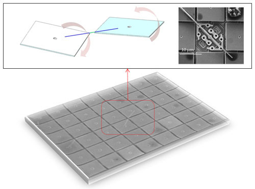
:
1. Introduction
2. Platform Development and Methodology
3. Platform Demonstration and Results
3.1. Demonstration of the Cyclic Loading with Different Loading Amplitudes
3.2. Demonstration of the Fatigue Failures of Nanowires under Cyclic Torsional Loading
3.3. Quantifying the Strain Distribution along the Nanowire under Torsion
4. Conclusions
Supplementary Materials
Acknowledgments
Author Contributions
Conflicts of Interest
References
- McAlpine, M.C.; Ahmad, H.; Wang, D. Highly ordered nanowire arrays on plastic substrates for ultrasensitive flexible chemical sensors. Nat. Mater. 2007, 6, 379–384. [Google Scholar] [PubMed]
- Nair, P.R.; Alam, M. Design considerations of silicon nanowire biosensors. IEEE Trans. Electron Devices 2007, 54, 3400–3408. [Google Scholar] [CrossRef]
- Fan, Z.; Ho, J.C.; Takahashi, T.; Yerushalmi, R.; Takei, K.; Ford, A.C.; Chueh, Y.L.; Javey, A. Toward the development of printable nanowire electronics and sensors. Adv. Mater. 2009, 21, 3730–3743. [Google Scholar] [CrossRef]
- Gudiksen, M.S.; Lauhon, L.J.; Wang, J.; Smith, D.C.; Lieber, C.M. Growth of nanowire superlattice structures for nanoscale photonics and electronics. Nature 2002, 415, 617–620. [Google Scholar] [CrossRef] [PubMed]
- Yao, J.; Yan, H.; Das, S.; Klemic, J.F.; Ellenbogen, J.C.; Lieber, C.M. Nanowire nanocomputer as a finite-state machine. Proc. Natl. Acad. Sci. USA 2014, 111, 2431–2435. [Google Scholar] [CrossRef] [PubMed]
- Uchic, M.D.; Dimiduk, D.M.; Florando, J.N.; Nix, W.D. Sample dimensions influence strength and crystal plasticity. Science 2004, 5686, 986–989. [Google Scholar] [CrossRef] [PubMed]
- Chang, P.C.; Chien, C.J.; Stichtenoth, D.; Ronning, C.; Lu, J.G. Finite size effect in ZnO nanowires. Appl. Phys. Lett. 2007, 90, 113101. [Google Scholar] [CrossRef]
- Wu, B.; Heidelberg, A.; Boland, J.J. Mechanical properties of ultrahigh-strength gold nanowires. Nat. Mater. 2005, 4, 525–529. [Google Scholar] [CrossRef] [PubMed]
- Zhu, T.; Li, J.; Ogata, S.; Yip, S. Mechanics of ultra-strength materials. MRS Bull. 2009, 34, 167–172. [Google Scholar] [CrossRef]
- Lu, Y.; Lou, J. Quantitative in-situ nanomechanical characterization of metallic nanowires. JOM 2011, 63, 35–42. [Google Scholar] [CrossRef]
- Gianola, D.S.; Eberl, C. Micro-and nanoscale tensile testing of materials. JOM 2009, 61, 24–35. [Google Scholar] [CrossRef]
- Boyce, B.; Huang, J.; Miller, D.; Kennedy, M. Deformation and failure of small-scale structures. JOM 2010, 4, 62–63. [Google Scholar] [CrossRef]
- Namazu, T.; Isono, Y. High-cycle fatigue test of nanoscale Si and SiO2 wires based on AFM technique. In Proceedings of the 16th IEEE Annual International Conference on Micro Electro Mechanical Systems (MEMS 2003), Kyoto, Japan, 19–23 January 2003; pp. 662–665.
- Gao, Z.; Ding, Y.; Lin, S.; Hao, Y.; Wang, Z.L. Dynamic fatigue studies of ZnO nanowires by in-situ transmission electron microscopy. Phys. Status Solidi RRL. 2009, 3, 260–262. [Google Scholar] [CrossRef]
- Li, P.; Liao, Q.; Yang, S.; Bai, X.; Huang, Y.; Yan, X.Q.; Zhang, Z.; Liu, S.; Lin, P.; Kang, Z.; et al. In situ transmission electron microscopy investigation on fatigue behavior of single ZnO wires under high-cycle strain. Nano Lett. 2014, 14, 480–485. [Google Scholar] [CrossRef] [PubMed]
- Ensslen, C.; Kraft, O.; Mönig, R.; Xu, J.; Zhang, G.P.; Schneider, R. Mechanical annealing of Cu–Si nanowires during high-cycle fatigue. MRS Commun. 2014, 4, 83–87. [Google Scholar] [CrossRef]
- Hosseinian, E.; Pierron, O.N. Quantitative in situ TEM tensile fatigue testing on nanocrystalline metallic ultrathin films. Nanoscale 2013, 5, 12532–12541. [Google Scholar] [CrossRef] [PubMed]
- Kumar, S.; Alam, M.T.; Haque, M.A. Fatigue Insensitivity of Nanoscale Freestanding Aluminum Films. J. Microelectromech. Syst. 2011, 20, 53–58. [Google Scholar] [CrossRef]
- Lu, Y.; Ganesan, Y.; Lou, J. A multi-step method for in situ mechanical characterization of 1-D nanostructures using a novel micromechanical device. Exp. Mech. 2010, 50, 47–54. [Google Scholar] [CrossRef]
- Haque, M.A.; Espinosa, H.D.; Lee, H.J. MEMS for in situ testing—Handling, actuation, loading, and displacement measurements. MRS Bull. 2010, 35, 375–381. [Google Scholar] [CrossRef]
- Pant, B.; Allen, B.L.; Zhu, T.; Gall, K.; Pierron, O.N. A versatile microelectromechanical system for nanomechanical testing. Appl. Phys. Lett. 2011, 98, 053506. [Google Scholar] [CrossRef]
- Saini, K.; Kumar, N. Torsional deformation behavior of cracked gold nano-wires. Acta Mech. 2014, 225, 687–700. [Google Scholar] [CrossRef]
- Jiang, S.; Zhang, H.; Zheng, Y.; Chen, Z. Atomistic study of the mechanical response of copper nanowires under torsion. J. Phys. D Appl. Phys. 2009, 42, 135408. [Google Scholar] [CrossRef]
- Gao, Y.; Wang, F.; Zhu, T.; Zhao, J. Investigation on the mechanical behaviors of copper nanowires under torsion. Comput. Mater. Sci. 2010, 49, 826–830. [Google Scholar] [CrossRef]
- Hornbeck, L.J. Digital light processing for high-brightness high-resolution applications. In Electronic Imaging'97; International Society for Optics and Photonics: Bellingham, WA, USA, 1997; pp. 27–40. [Google Scholar]
- Douglass, M.R. Lifetime estimates and unique failure mechanisms of the digital micromirror device (DMD). In Proceedings of the 36th Annual IEEE International Reliability Physics Symposium, Reno, NV, USA, 31 March–2 April 1998; pp. 9–16.
- Dudley, D.; Duncan, W.M.; Slaughter, J. Emerging digital micromirror device (DMD) applications. In Micromachining and Microfabrication; International Society for Optics and Photonics: Bellingham, WA, USA, 2003; pp. 14–25. [Google Scholar]


© 2016 by the authors. Licensee MDPI, Basel, Switzerland. This article is an open access article distributed under the terms and conditions of the Creative Commons by Attribution (CC-BY) license ( http://creativecommons.org/licenses/by/4.0/).
Share and Cite
Jiang, C.; Hu, D.; Lu, Y. Digital Micromirror Device (DMD)-Based High-Cycle Torsional Fatigue Testing Micromachine for 1D Nanomaterials. Micromachines 2016, 7, 49. https://doi.org/10.3390/mi7030049
Jiang C, Hu D, Lu Y. Digital Micromirror Device (DMD)-Based High-Cycle Torsional Fatigue Testing Micromachine for 1D Nanomaterials. Micromachines. 2016; 7(3):49. https://doi.org/10.3390/mi7030049
Chicago/Turabian StyleJiang, Chenchen, Dayong Hu, and Yang Lu. 2016. "Digital Micromirror Device (DMD)-Based High-Cycle Torsional Fatigue Testing Micromachine for 1D Nanomaterials" Micromachines 7, no. 3: 49. https://doi.org/10.3390/mi7030049