
Fabrication of Functional Plastic Parts Using Nanostructured Steel Mold Inserts

Abstract
:
1. Introduction
2. Materials and Methods
2.1. Steel Substrate Preparation
2.2. Surface Nanostructuring
2.3. Hot Embossing and Injection Molding
2.4. Surface Characterization
2.5. Wettability Measurements
2.6. Immunoassay
3. Results and Discussion
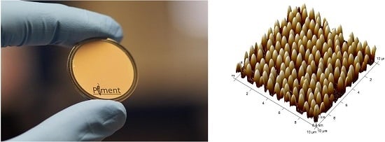
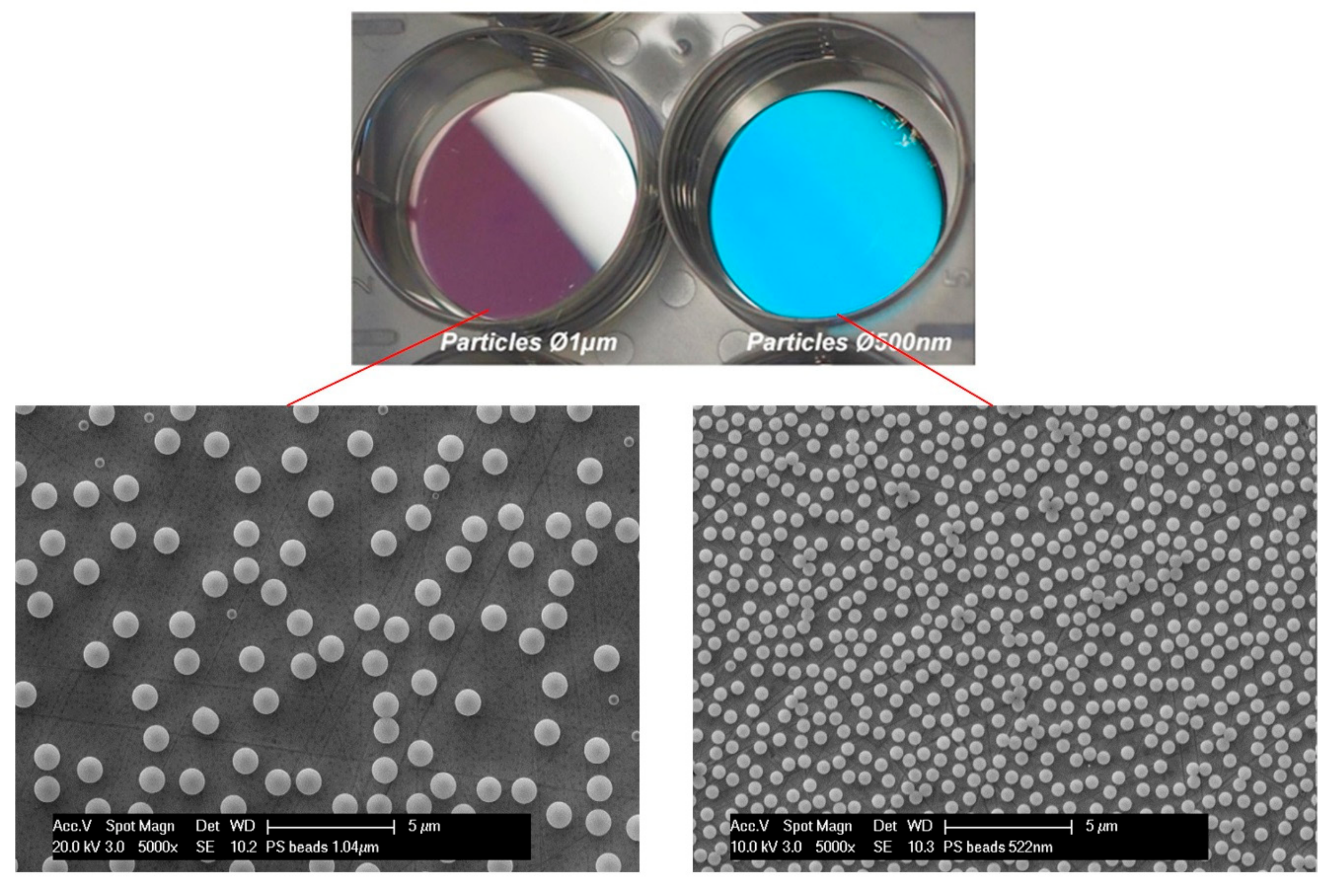
3.1. Surface Structuring of Flat Stainless Steel (2D Substrate)
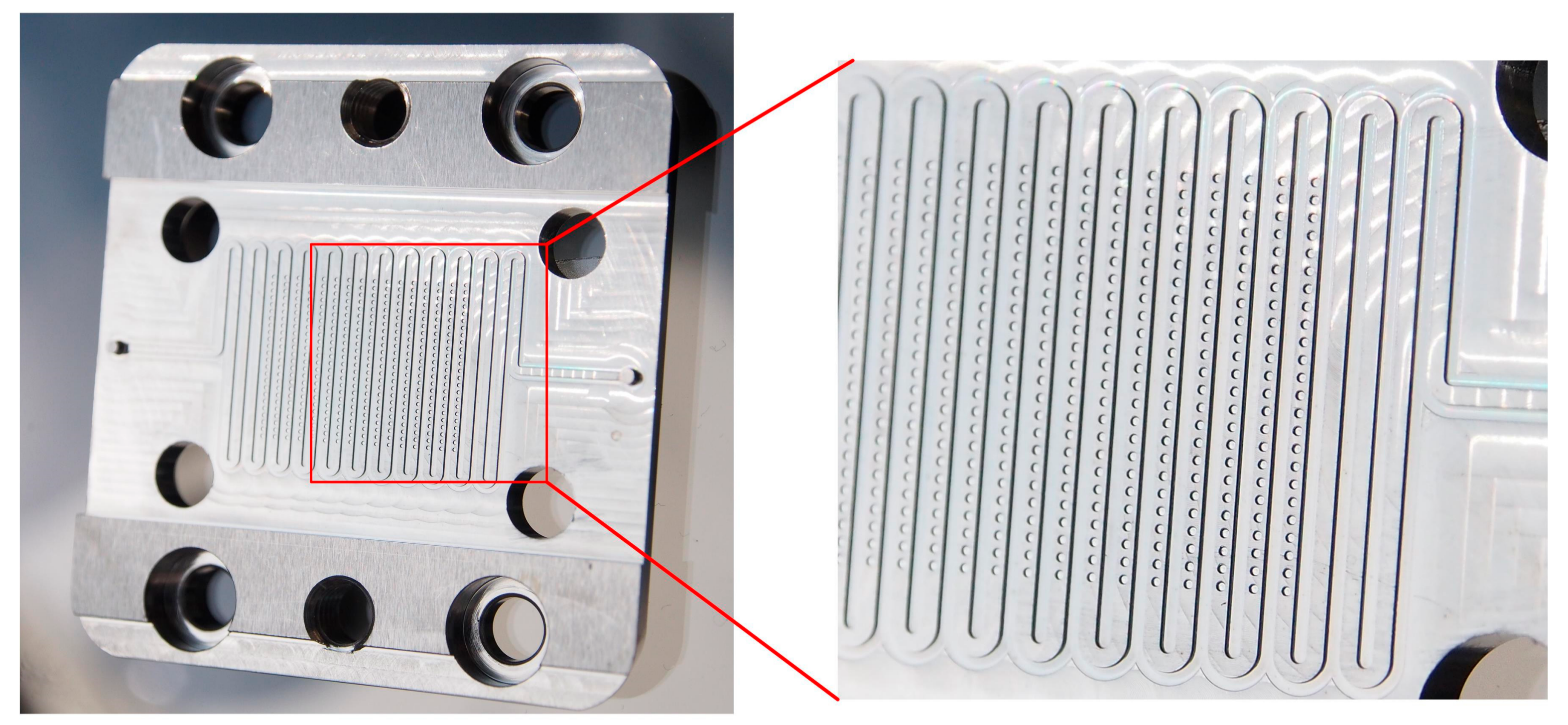
3.2. Surface Nanostructuring of the Microstructured Insert (3D Substrate)
3.3. Hot Embossing and Injection Molding of Plastic Parts
3.4. Characterization
3.4.1. Surface Characterization
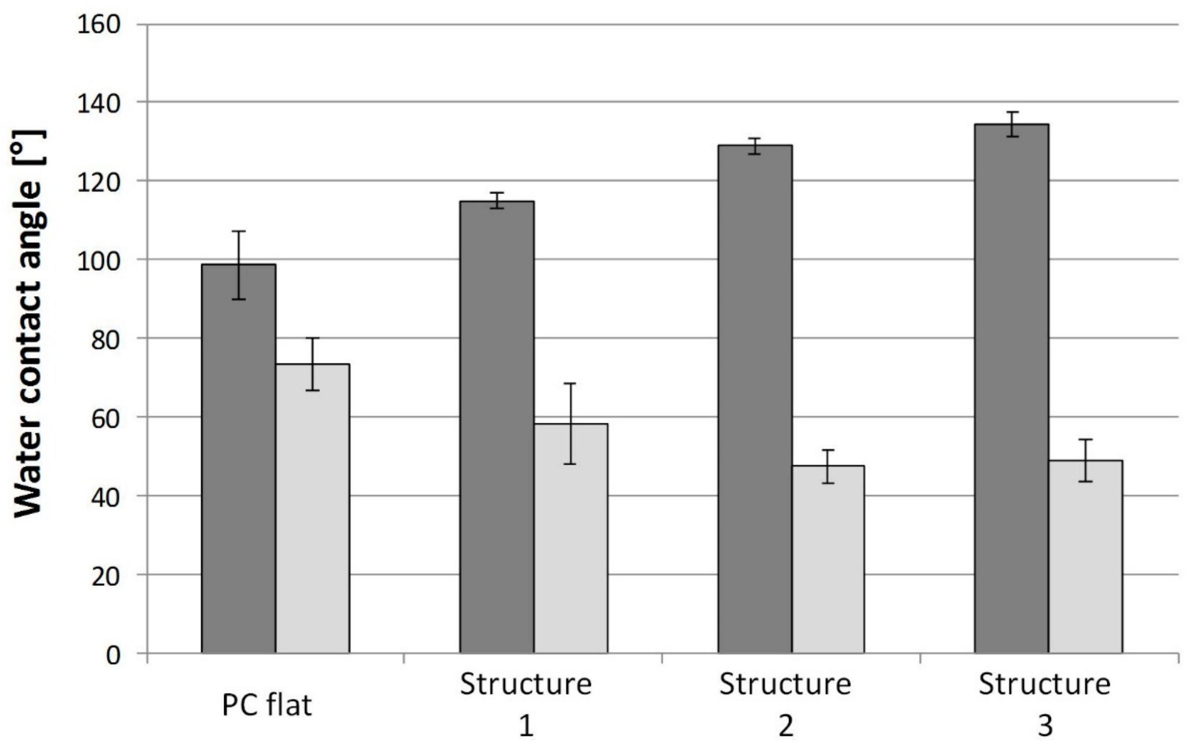
3.4.2. Wettability
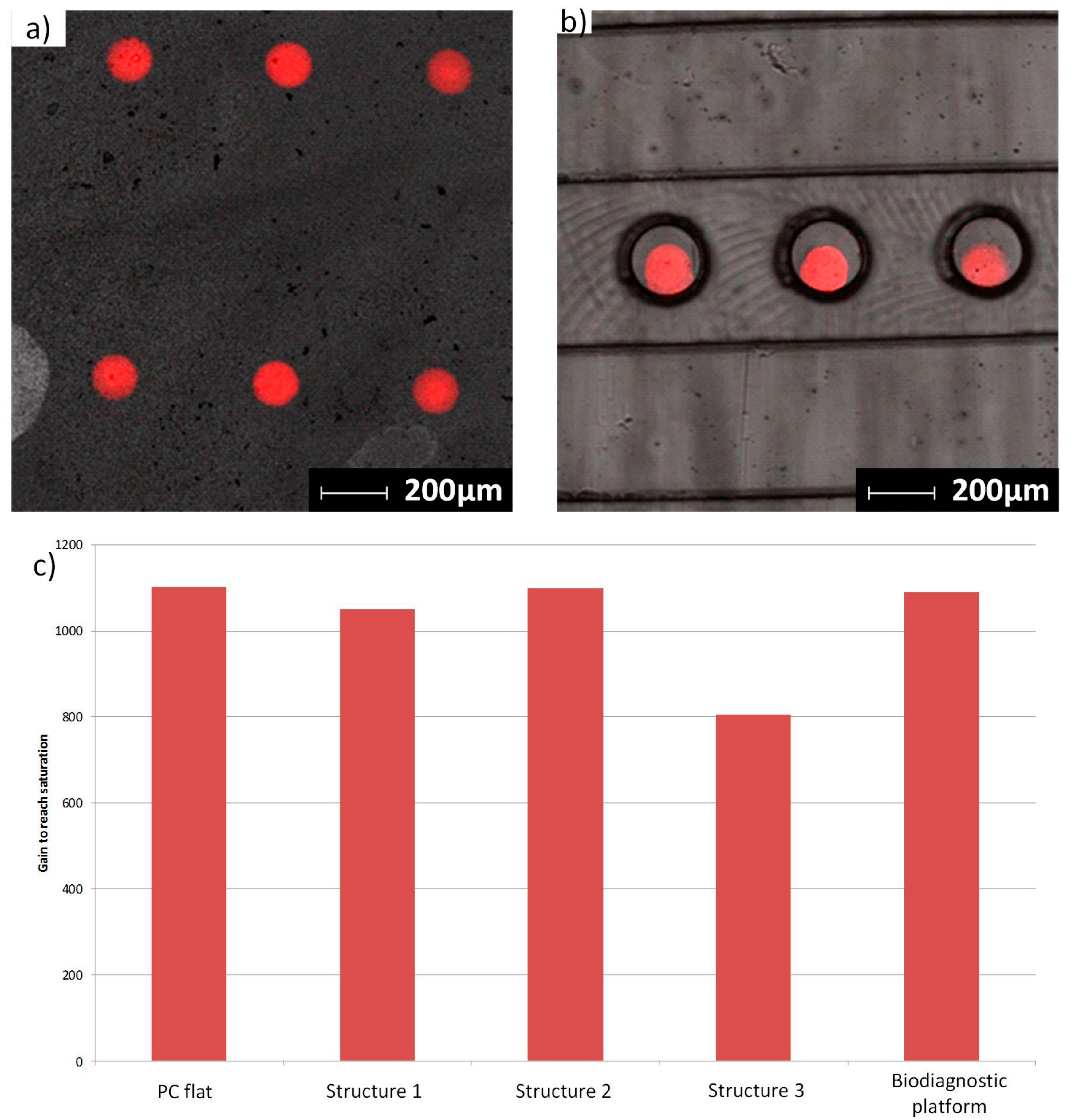
3.4.3. Immunoassay
4. Conclusions
Acknowledgments
Author Contributions
Conflicts of Interest
References
- Kim, S.; Jung, U.T.; Kim, S.K.; Lee, J.H.; Choi, H.S.; Kim, C.S.; Jeong, M.Y. Nanostructured Multifunctional Surface with Antireflective and Antimicrobial Characteristics. Appl. Mater. Interfaces 2015, 7, 326–331. [Google Scholar] [CrossRef] [PubMed]
- Weder, G.; Blondiaux, N.; Giazzon, M.; Matthey, N.; Klein, M.; Pugin, P.; Heinzelmann, H.; Liley, M. Use of Force Spectroscopy to Investigate the Adhesion of Living Adherent Cells. Langmuir 2010, 26, 8180–8186. [Google Scholar] [CrossRef] [PubMed]
- Roch, T.; Weihnacht, V.; Scheibe, H.J.; Roch, A.; Lasagni, A.F. Direct Laser Interference Patterning of tetrahedral amorphous carbon films for tribological applications. Diam. Relat. Mater. 2013, 33, 20–26. [Google Scholar] [CrossRef]
- Quéré, D. Wetting and roughness. Annu. Rev. Mater. Res. 2008, 38, 71–99. [Google Scholar] [CrossRef]
- Blondiaux, N.; Scolan, E.; Popa, A.M.; Gavillet, J.; Pugin, R. Fabrication of superhydrophobic surfaces with controlled topography and chemistry. Appl. Surf. Sci. 2009, 256, S46–S53. [Google Scholar] [CrossRef]
- Spori, D.; Drobek, T.; Zürcher, S.; Spencer, N.D. Cassie-State wetting investigated by means of holes to pillar density gradient. Langmuir 2010, 26, 9465–9473. [Google Scholar] [CrossRef] [PubMed]
- Martines, E.; Seunarine, K.; Morgan, H.; Gadegaard, N.; Wilkinson, C.D.W.; Riehle, M.O. Superhydrophobicity and superhydrophilicity of regular nanopatterns. Nano Lett. 2005, 5, 2097–2103. [Google Scholar] [CrossRef] [PubMed]
- Blondiaux, N.; Scolan, E.; Franc, G.; Pugin, R. Manufacturing of super-hydrophobic surfaces combining nanosphere lithography with replication techniques. Nanotechnology 2012, 1–6. [Google Scholar] [CrossRef]
- Krishnamoorthy, S. Nanostructured sensors for biomedical applications—A current perspective. Curr. Opin. Biotechnol. 2015, 34, 118–124. [Google Scholar] [CrossRef] [PubMed]
- Stewart, M.E.; Anderton, C.R.; Thompson, L.B.; Maria, J.; Gray, S.K.; Rogers, J.A.; Nuzzo, R.G. Nanostructured plasmonic sensors. Chem. Rev. 2008, 108, 494–521. [Google Scholar] [CrossRef] [PubMed]
- Ko, H.; Singamaneni, S.; Tsukruk, V.V. Nanostructured surfaces and assemblies as SERS media. Small 2008, 4, 1576–1599. [Google Scholar] [CrossRef] [PubMed]
- Kanipe, K.N.; Chidester, P.P.F.; Stucky, G.D.; Moskovits, M. Large format surface-enhanced Raman spectroscopy substrate optimized for enhancement and uniformity. ACS Nano 2016, 10, 7566–7571. [Google Scholar] [CrossRef] [PubMed]
- Ingham, C.J.; Maat, J.; De Vos, W.M. Where bio meets nano: The many uses for nanoporous aluminum oxide in biotechnology. Biotechnol. Adv. 2012, 30, 1089–1099. [Google Scholar] [CrossRef] [PubMed]
- Kim, J.S.; Chob, J.B.; Park, B.G.; Leed, W.; Lee, K.B.; Oh, M.K. Size-controllable quartz nanostructure for signal enhancement of DNA chip. Biosens. Bioelectron. 2011, 26, 2085–2089. [Google Scholar] [CrossRef] [PubMed]
- Kuwabara, K.; Ogino, M.; Ando, T.; Miyauchi, A. Enhancement of fluorescence intensity from an immunoassay chip using high-aspect-ratio nanopillars fabricated by nanoimprinting. Appl. Phys. Lett. 2008, 93, 3. [Google Scholar] [CrossRef]
- Masuzawa, T. State of the Art of Micromachining. Ann. CIRP 2000, 49, 473–488. [Google Scholar] [CrossRef]
- Bieda, M.; Schmädicke, C.; Roch, T.; Lasagni, A. Ultra-low friction on 100Cr6-steel surfaces after direct laser interference patterning. Adv. Eng. Mater. 2015, 17, 102–108. [Google Scholar] [CrossRef]
- Madou, M. Fundamentals of Microfabrication: The Science of Miniaturization; CRC Press: Boca Raton, FL, USA, 2002. [Google Scholar]
- Pease, R.F.; Chou, S.Y. Lithography and other patterning techniques for future electronics. Proc. IEEE 2008, 96, 248–270. [Google Scholar] [CrossRef]
- Ruiz, R.; Kang, H.; Detcheverry, F.A.; Dobisz, E.; Kercher, D.S.; Albrecht, T.R.; De Pablo, J.J.; Nealey, P.F. Density multiplication and improved lithography by directed block copolymer assembly. Science 2008, 321, 936–939. [Google Scholar] [CrossRef] [PubMed]
- Klein, M.J.K.; Montagne, F.; Blondiaux, N.; Vazquez-Mena, O.; Heinzelmann, H.; Pugin, R.; Brugger, J.; Savu, V. SiN membranes with submicrometer hole arrays patterned by wafer-scale nanosphere lithography. J. Vac. Sci. Technol. B 2011, 2, 021012. [Google Scholar] [CrossRef]
- Hao, L.; Meng, Y.; Chen, C. Experimental investigation on effects of surface texturing on lubrication of initial line contacts. Lubr. Sci. 2014, 26, 363–373. [Google Scholar] [CrossRef]
- Mason, J.A.; Adams, D.C.; Johnson, Z.; Smith, S.; Davis, A.W.; Wasserman, D. Selective thermal emission from patterned steel. Opt. Express 2010, 18, 25192. [Google Scholar] [CrossRef] [PubMed]
- Rao, P.N.; Kunzru, D. Fabrication of microchannels on stainless steel by wet chemical etching. J. Micromech. Microeng. 2007, 17, 99–106. [Google Scholar]
- Landolt, D.; Chauvy, P.F.; Zinger, O. Electrochemical micromachining, polishing and surface structuring of metals: Fundamental aspects and new developments. Electrochim. Acta 2003, 48, 3185–3201. [Google Scholar] [CrossRef]
- Zinger, O.; Chauvy, P.F.; Landolt, D. Development of titatnium electrochemical microstructuring towards implant applications. Eur. Cells Mater. 2001, 1, 24–25. [Google Scholar]
- Zinger, O.; Chauvy, P.F.; Landolt, D. Scale-resolved electrochemical surface structuring of titanium for biological applications. J. Electrochem. Soc. 2003, 150, B495–B503. [Google Scholar] [CrossRef]
- Shimizu, M.; Yamada, T.; Sasaki, K.; Takada, A.; Nomura, H.; Iguchi, F.; Yugami, H. Anisotropic multi-step etching for large-area fabrication of surface microstructures on stainless steel to control thermal radiation. Sci. Technol. Adv. Mater. 2015, 16, 025001–025006. [Google Scholar] [CrossRef] [PubMed]
- Al-Azawi1, A.; Smistrup, K.; Kristensen, A. Nanostructuring steel for injection molding tools. J. Micromech. Microeng. 2014, 24, 055023–055029. [Google Scholar] [CrossRef]
- Kurihara, K.; Saitou, Y.; Souma, N.; Makihara, S.; Kato, H.; Nakano, T. Fabrication of nano-structure anti-reflective lens using platinum nanoparticles in injection moulding. Mater. Res. Express 2015, 2, 015008. [Google Scholar] [CrossRef]
- Guillaumée, M.; Liley, M.; Pugin, R.; Stanley, R. Scattering of light by a single layer of randomly packed dielectric microspheres giving color effects in transmission. Opt. Express 2008, 16, 1440–1447. [Google Scholar] [CrossRef] [PubMed]
- Scopelliti, P.E.; Borgonovo, A.; Indrieri, M.; Indrieri, M.; Giorgetti, L.; Bongiorno, G.; Carbone, R.; Podesta, A.; Milani, P. The Effect of Surface Nanometre-Scale Morphology on Protein Adsorption. PLoS ONE 2010, 5, 11862. [Google Scholar] [CrossRef] [PubMed]
- Yasuda, M.; Akimoto, T. Highly Sensitive Fluorescence Detection of Avidin/Streptavidin with an Optical Interference Mirror Slide. Anal. Sci. 2012, 28, 947–952. [Google Scholar] [CrossRef] [PubMed]


| ID | RMS Roughness (nm) | Surface Area Difference (%) | Feature Density (part/cm2) | Average Feature Diameter (nm) | Average Feature Height (nm) |
|---|---|---|---|---|---|
| Structure 1 | 143 | 14.7 | 1.5e7 | 1249 | 516 |
| Structure 2 | 107 | 33.3 | 1.37e8 | 753 | 287 |
| Structure 3 | 121 | 37.3 | 1.34e8 | 914 | 360 |
© 2017 by the authors. Licensee MDPI, Basel, Switzerland. This article is an open access article distributed under the terms and conditions of the Creative Commons Attribution (CC BY) license (http://creativecommons.org/licenses/by/4.0/).
Share and Cite
Blondiaux, N.; Pugin, R.; Andreatta, G.; Tenchine, L.; Dessors, S.; Chauvy, P.-F.; Diserens, M.; Vuillermoz, P. Fabrication of Functional Plastic Parts Using Nanostructured Steel Mold Inserts. Micromachines 2017, 8, 179. https://doi.org/10.3390/mi8060179
Blondiaux N, Pugin R, Andreatta G, Tenchine L, Dessors S, Chauvy P-F, Diserens M, Vuillermoz P. Fabrication of Functional Plastic Parts Using Nanostructured Steel Mold Inserts. Micromachines. 2017; 8(6):179. https://doi.org/10.3390/mi8060179
Chicago/Turabian StyleBlondiaux, Nicolas, Raphaël Pugin, Gaëlle Andreatta, Lionel Tenchine, Stéphane Dessors, Pierre-François Chauvy, Matthieu Diserens, and Philippe Vuillermoz. 2017. "Fabrication of Functional Plastic Parts Using Nanostructured Steel Mold Inserts" Micromachines 8, no. 6: 179. https://doi.org/10.3390/mi8060179