3.1. Voltage and Current Characteristics of C2H2 Plasma Jet in Vacuum
Figure 3 shows the current and voltage plots and
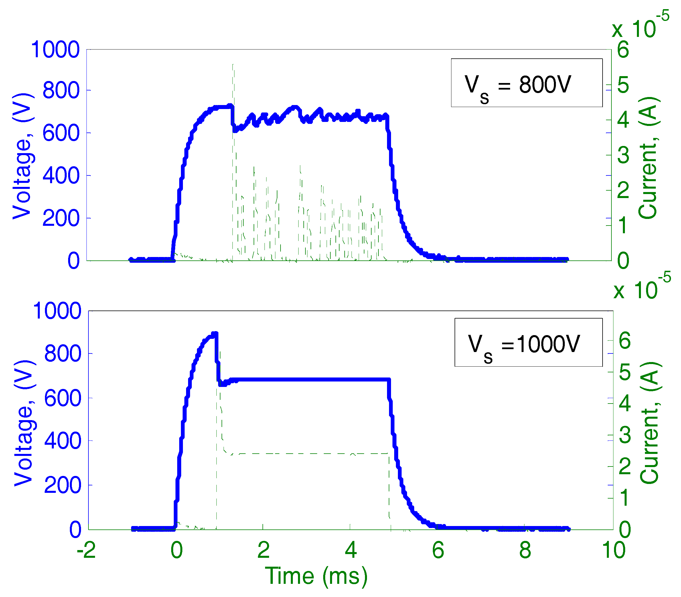
Figure 4 shows typical waveforms of voltage and current during an intentionally modulated pulse voltage at 6.6 sccm C
2H
2 flow rate (about 80 kPa inlet pressure). As shown in
Figure 4, the discharge was automatically pulsing even if the source voltage was continuously applied at 800 V while it was quite stable at 1000 V. The two different types of discharge modes—self-pulsing mode and continuous mode—are similar to those in previous reports [
10,
11,
12]. In our previous work, it had been confirmed that the continuous discharge mode was suitable for plasma processing such as micro sputter etching due to their stability [
13].
Figure 3 shows current and voltage characteristics with a variation of gap distance from 100 to 200 μm. Two discharge modes are separated by each threshold of minimum discharge current for sustaining continuous discharge (
Imin), which is depicted by short thin vertical lines. The threshold current depends on the gas type, pressure and gas flow rate, electrode gap distance, electrode material, and other conditions. In the experimental results, the thresholds were 15.5, 16, and 11 μA for the gap distance of 100, 150, and 200 μm, respectively. At a current above the threshold, the discharge voltage was almost constant as expected for normal glow discharge scheme. By increasing the source voltage while the discharge voltage was almost constant, the discharge current increased as the voltage drop of the ballast resistor increased. In
Figure 4, typical waveforms of current and voltage at 150 μm gap distance are shown. The required threshold current for continuous discharge was not supplied through the ballast resistor when the source voltage was 800 V while a sufficient current was supplied when the source voltage was increased to 1000 V.
The self-pulsing discharge is characterized by breakdown voltage (
VBR) and recovery voltage (
VRE). The recovery voltage is the minimum and the breakdown voltage is the maximum in the voltage waveform during self-pulsing discharge which are required for sustaining and igniting discharge, respectively [
13]. The voltage waveform oscillates between these two voltages.
The self-pulsing of discharge is induced in an RC circuit consisting of the ballast resistor and a stray capacitor of anode wiring. The detailed explanation of self-pulsing discharge was explained in literature [
12]. The current from the voltage source is limited by the large ballast resistor. The current limit depends on the resistance value and on the voltage drop as the difference between voltage source and required discharge voltage. When a discharge started at the breakdown voltage with insufficient current supply through the ballast resistor, only for a short duration, the gas discharge can be continued by the current from the stray capacitor. By discharging the stray capacitor, however, the anode voltage quickly dropped, resulting in automatic termination of gas discharge. In turn, after termination, the stray capacitor is charged again through the ballast resistor until the voltage reaches the breakdown voltage.
Due to deposition of film from C
2H
2 source gas on the Si wafer as cathode, the voltage and current characteristic drifted with discharge and deposition duration.
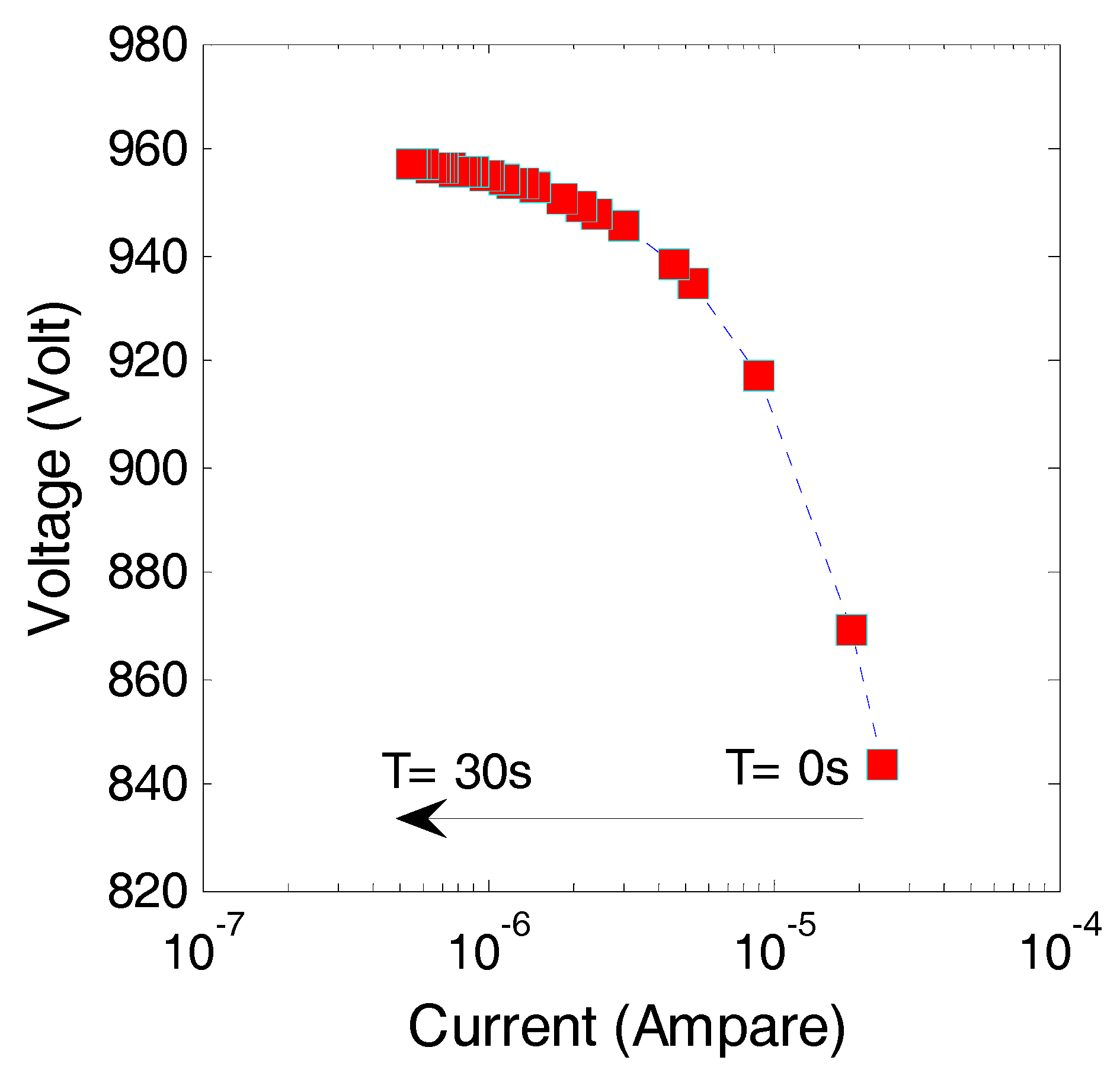
Figure 5 shows the DC (time averaged) current and voltage plots by sampling every 0.5 s for 30 s in total at the electrode gap distance of 150 μm and at a continuous source voltage of 1000 V. The C
2H
2 discharge was automatically terminated after a few tens of seconds from the ignition of discharge with a virgin Si wafer. At this experimental condition, C
2H
2 plasma started at 845 V with a current of 24 μA. The continuous discharge mode was sustained only for a few milliseconds after ignition and quickly turned to the self-pulsing discharge mode. With the discharge and deposition, the voltage increased and the current decreased. After 15 s of discharge, the voltage increased to 955 V while the current decreased to 1.5 μA.
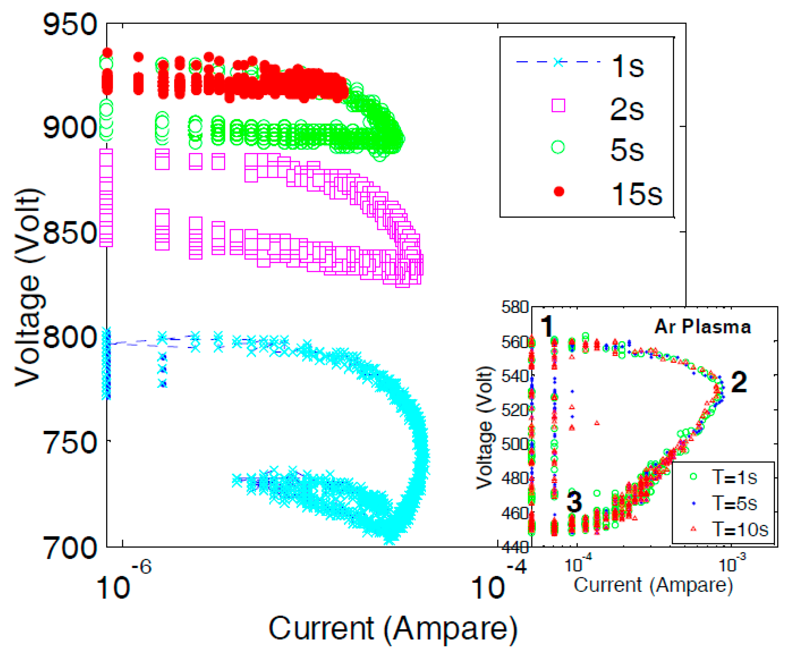
Figure 6 shows the plots of instantaneous current and voltage during self-pulsing discharge at different elapsed time, 1, 2, 5, and 15 s from ignition of C
2H
2 plasma at the electrode gap distance of 150 μm and the continuous source voltage of 1000 V.
The inset in
Figure 6 shows the plots of instantaneous current and voltage during self-pulsing discharge with Ar plasma jet at elapsed time 1, 2, and 5 s from ignition. The self-pulsing mode of Ar plasma jet could be separated into three phases per cycle [
9,
14]. During the self-pulsing, each pulse discharge started at the breakdown voltage and almost negligible current (mostly due to electric noise), as indicated “1” in the inset figure, the current increased to the peak, as indicated point “2”. During the discharge from point “1” to point “3”, the anode voltage dropped by discharging the stray capacitor to continue the instantaneous discharge. The discharge automatically terminates at the minimum sustain voltage (recovery voltage), as indicated point “3”, and the stray capacitor is charged until the next breakdown at point “1”. In the case of Ar discharge, the cycles of self-pulsing discharge repeated in the same way for a long duration. In the case of C
2H
2 plasma jet, the plots of self-pulsing cycle gradually shifted to the higher voltage side due to an increase in both breakdown voltage and sustain voltage.
It was confirmed that the deposited film was highly insulated due to charge up of the surface during SEM observation. The effect of the insulating cathode surface on the discharge property is a drawback of DC gas discharge [
15]. Moreover, local heating and arcing will result in degrading film properties and formation of micro particle on the surface [
16]. Insulating film deposition on the electrode strongly affected the gas discharge properties not only by blocking the current flow but also by substitution of surface properties [
17].
When the film thickness is still thin enough to permit a small amount of current flow in the film bulk, the deposited film simply performs as a series resistance. Due to the voltage drop that appeared in the film bulk, the apparent working voltage will increase. By increasing the operation duration, the film thickness will increase and the voltage drop will also increase. Due to increase of the voltage drop in the film as the series resistance, the voltage for the ballast resistor decreased instead at the constant source voltage and even at the constant gas discharge voltage. In the experiments, after a few milliseconds of operation, the discharge mode turned to the self-pulsing because the voltage for the ballast resistor decreased, resulting in a severe current limit.
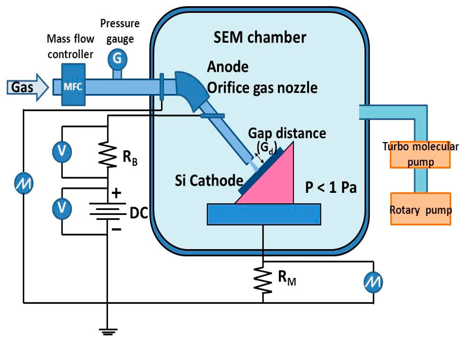
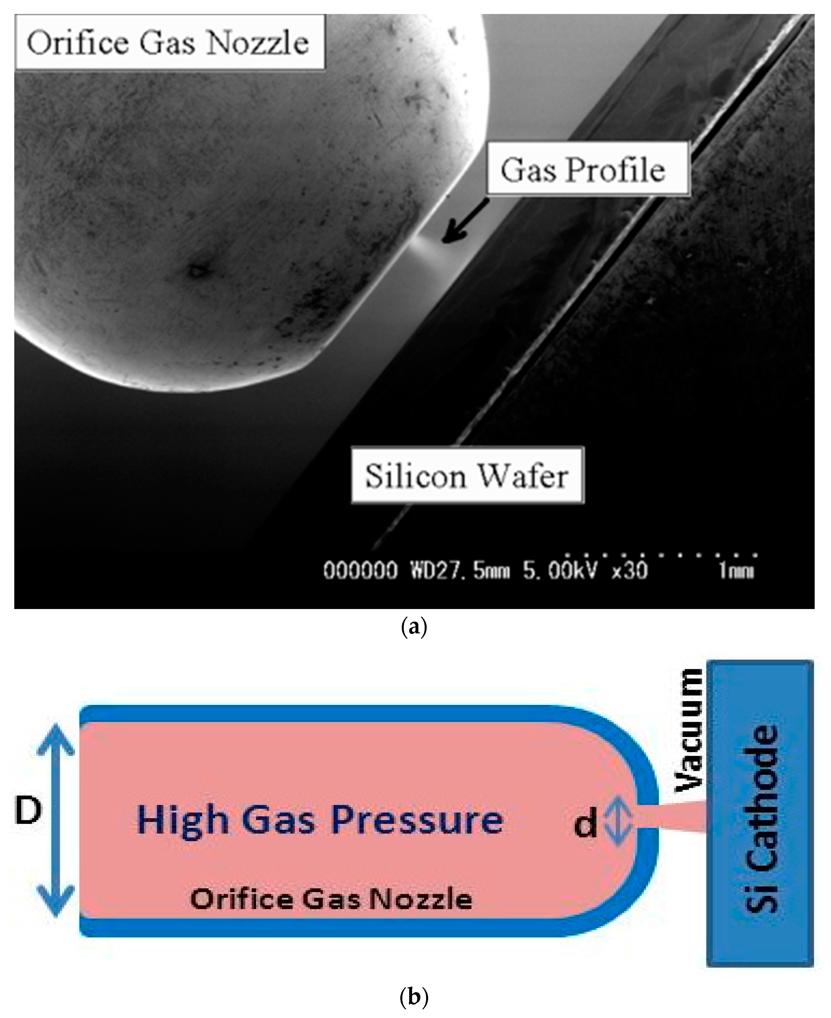
In the case of this micro plasma jet, it is also important to consider the local profile of film deposition. Due to the extreme gas profile, as shown in
Figure 2a, the gas discharge current pass and the excited plasma profile will be localized only in the high density gas jet at first. As mentioned in the next section, the film deposition is also limited in the local area irradiated to the high pressure gas spraying. When the high pressure gas spraying area is fully covered with insulating film, it cannot work as a cathode and gas discharge should be sustained in the surrounding area where the gas density dramatically decrease by rapid diffusion into the vacuum environment. Moreover, the pass length from the anode to the working cathode area becomes much longer than the configured gap length. Due to an increase of the actual discharge pass length and the dramatic decrease of gas pressure on the working cathode area, the breakdown voltage and sustain voltage increase substantially. A possible solution for sustaining discharge through the insulating film is using AC, RF, and pulse DC power [
7,
16,
17,
18].
3.2. Properties of Deposited Thin Films
On the Si wafer as cathode, an insulating film was deposited during operation of the C
2H
2 plasma jet. The reactions at the growing film surface occurred as a result of interactions between the silicon substrate and the ions, radicals, atoms, and gas molecules in the plasma [
19,
20,
21]. For analysis on film properties, films were deposited at the gap distance of 100 and 200 μm, C
2H
2 flow rate of 6.6 sccm, inlet gas pressure of 80 kPa, and source voltage of 1000 V.
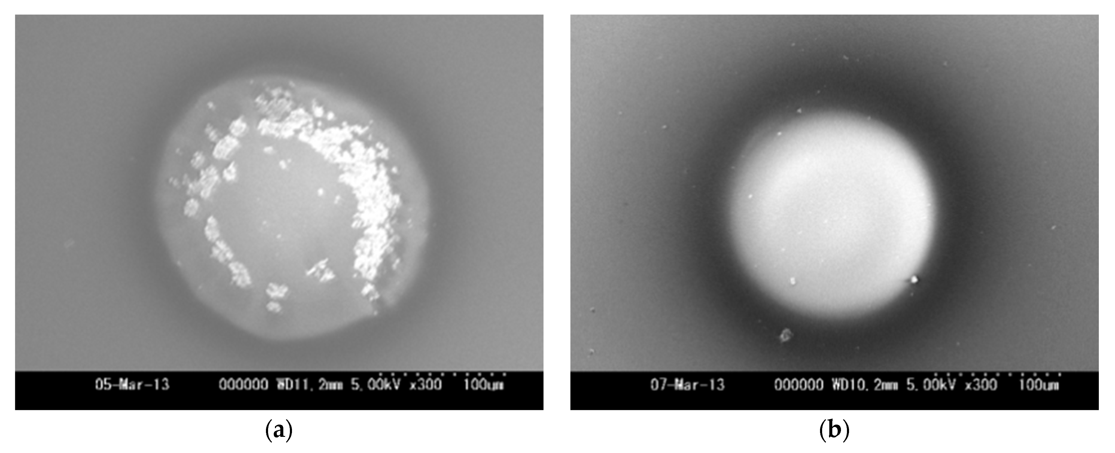
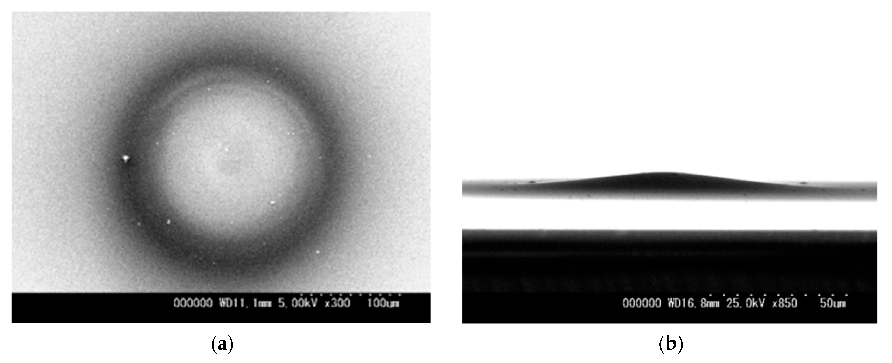
Figure 7a,b show the SEM images of Si wafers as cathode after 5 s operation at 100 and 200 μm in gap length with 38 and 19 μA of initial current, respectively. As shown in
Figure 7a, there were many clusters or flakes on the film in the case of the 100 μm gap length. In the case of the 200 μm gap length, the surface looked almost smooth. Though the detail structure of the flakes has not clarified yet, the local high electric field would induce focusing of current with resulting in breaking films and formation of micro particles [
16].
Figure 8a,b show SEM images of a deposited film on Si wafer from top view and side view, respectively, after 15 s operation at 200 μm gap length, 6.6 sccm C
2H
2 flow rate with 80 kPa inlet pressure, 1000 V source voltage and 19 μA initial discharge current.
Figure 9 shows an optical microscope image for the deposited film. The deposited film was not uniform but circularly-shaped with a diameter of 220 μm. As shown in
Figure 8b, the deposited film was fairly thick as directly recognized from the tilted angle observation. From the multiple concentric rings for optical interference in the film appeared in
Figure 9, the profile was a symmetric shallow mountain shape.
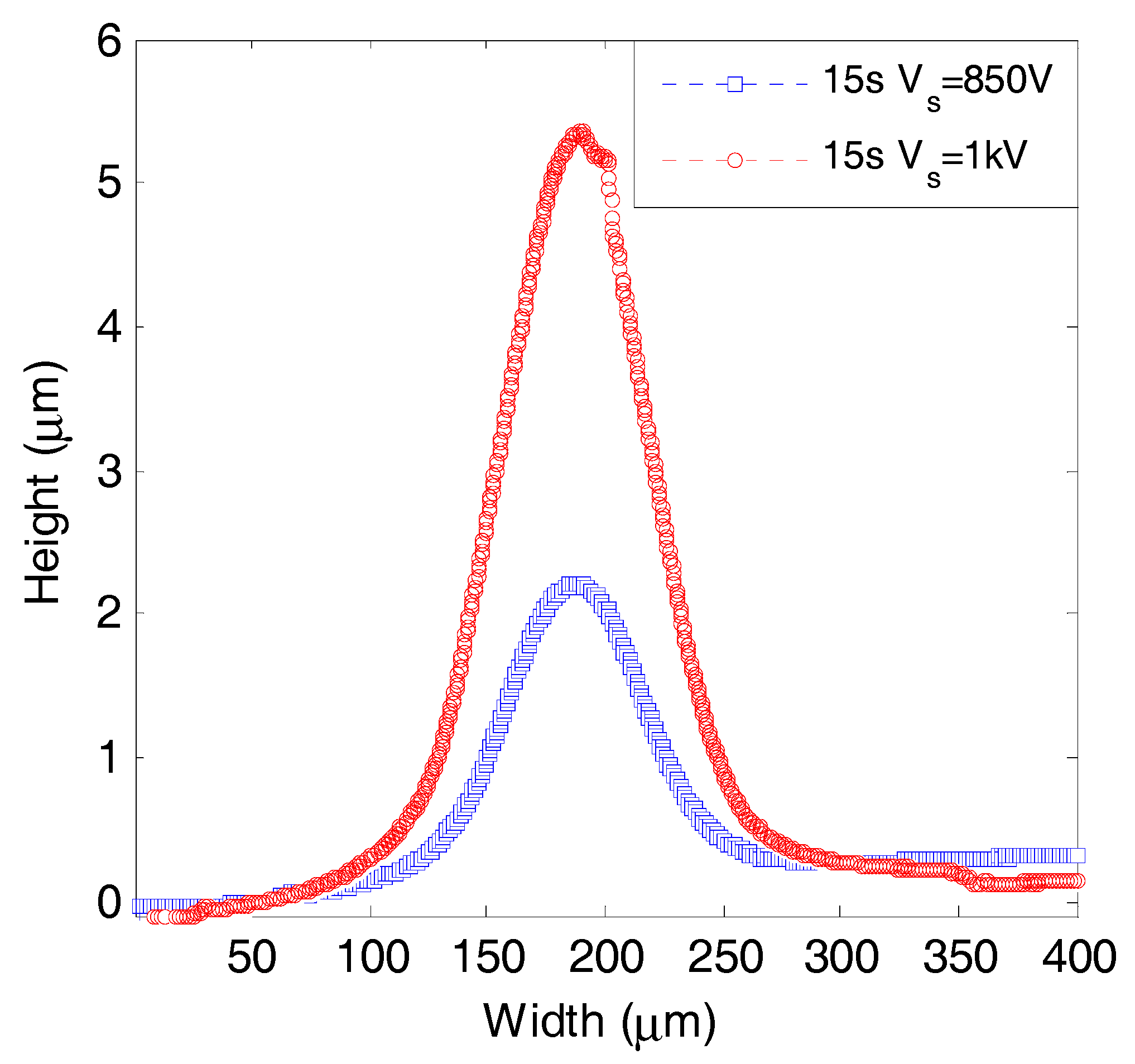
Figure 10 shows thickness profile of films on Si wafer deposited for 15 s at 200 μm gap length, 6.6 sccm C
2H
2 flow rate with 80 kPa inlet pressure, 850 or 1000 V source voltage with 13 or 19 μA initial current, respectively. The sizes of the deposited areas were evaluated as 175 and 220 μm for 850 and 1000 V, respectively. With increasing the source voltage, the deposition area was enlarged. As mentioned in the previous section, when the central area was fully covered with insulating film, the surrounding area of the Si wafer worked as a cathode. In the surrounding area, however, it required a higher voltage for discharge due to the longer pass and the dramatically decreased pressure. By applying a higher source voltage, the gas discharge can be sustained at farther distance from the center, resulting in a larger deposition area.
The deposition rates at the central position were evaluated as 0.15 and 0.33 μm/s for 850 and 1000 V source voltage, respectively. The deposition rates of this micro plasma jet were much higher than those by the conventional PECVD method by almost 10 times [
21]. From the discussion in the previous section, the plasma would be focused in the central area at the beginning of discharge due to higher gas pressure than the surrounding area. Due to progress in deposition at the central area, the plasma profile would move to the surrounding area. It can be speculated that the deposition rate is not constant at each position, but gradually changes with the progress of deposition.
It was confirmed that a symmetrical profile thick film was automatically achieved within a short duration by the presented micro gas jet configuration without any complex design [
22]. The smooth, symmetric, and fast film deposition will be advantageous for application to electronic devices.
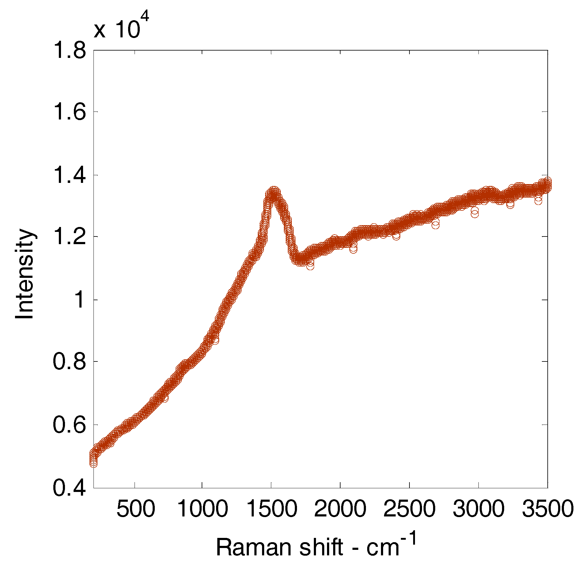
Figure 11 shows a typical Raman spectrum for a film deposited for 15 s at 200 μm gap, 6.6 sccm C
2H
2 flow rate, 80 kPa inlet pressure, and 1000 V source voltage. The Raman spectrum shows a peak of G band and D band, which originate from hydrogenated amorphous carbon film (a-C:H), at around 1521 cm
−1 and 1367 cm
−1, respectively. The ratio of the D and G band intensities (I
D/I
G ratio) indicated that a-C:H film was structurally similar to DLC films [
23]. At this experimental condition, the I
D/I
G ratio was approximately 0.8517, which was smaller than that of some conditions of a-C:H films grown by dip-coating, pulsed laser deposition, and PECVD methods of [
23,
24].
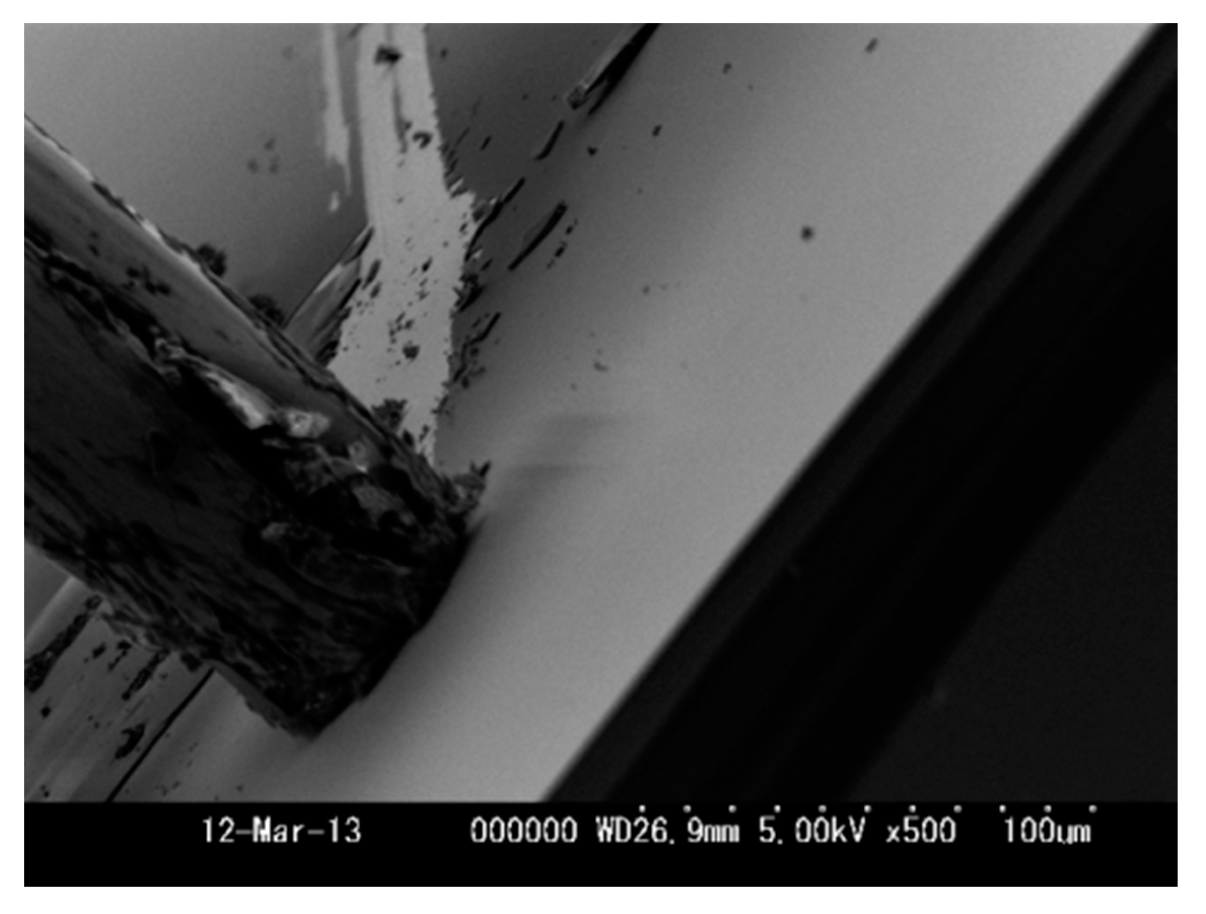
After that, the film hardness and adhesion to the Si wafer were simply examined by scratching with a tungsten (W) needle in SEM as shown in
Figure 12. The end of needle was a round column, 30 μm in diameter. With observation of the SEM image, the needle was pressed vertically on the film for indentation test and was scratched horizontally on the surface. By pressing on the film, the smooth surface was not damaged due to sufficient hardness for the compressive stress. By scratching on the surface, however, the film was peeled from the interface of the Si wafer. Since the deposition parameters—such as the operating pressure, C
2H
2 concentration, and depositing time—have strongly influenced on the quality of thin-film, how to improve the film quality by our proposed method will be studied in further work.


