Step-Double-Zone-JTE for SiC Devices with Increased Tolerance to JTE Dose and Surface Charges

Key Laboratory of RF Circuits and Systems, Ministry of Education, Hangzhou Dianzi University, Hangzhou 310018, China
*
Author to whom correspondence should be addressed.
Micromachines 2018, 9(12), 610; https://doi.org/10.3390/mi9120610
Submission received: 10 October 2018
/
Revised: 12 November 2018
/
Accepted: 20 November 2018
/
Published: 22 November 2018
(This article belongs to the Special Issue Wide Bandgap Semiconductor Based Micro/Nano Devices)
Abstract
:In this paper, an edge termination structure, referred to as step-double-zone junction termination extension (Step-DZ-JTE), is proposed. Step-DZ-JTE further improves the distribution of the electric field (EF) by its own step shape. Step-DZ-JTE and other termination structures are investigated for comparison using numerical simulations. Step-DZ-JTE greatly reduces the sensitivity of breakdown voltage (BV) and surface charges (SC). For a 30-μm thick epi-layer, the optimized Step-DZ-JTE shows 90% of the theoretical BV with a wide tolerance of 12.2 × 1012 cm−2 to the JTE dose and 85% of the theoretical BV with an improved tolerance of 3.7 × 1012 cm−2 to the positive SC are obtained. Furthermore, when combined with the field plate technique, the performance of the Step-DZ-JTE is further improved.
1. Introduction
Silicon carbide (SiC), a representative of the third generation of semiconductor materials, is a promising candidate for power devices due to its superior properties such as wide bandgap, high breakdown electric field, high thermal conductivity, and high drift saturation speed [1,2,3,4,5]. Hence, SiC devices are more suitable than silicon counterparts for high-voltage, high-frequency, and high-temperature applications. However, the potential performance (e.g., high blocking) of SiC materials is limited due to the presence of the effect of field crowding at the device edge.
To achieve high breakdown voltages (BV) for the planar junction close to its theoretical voltage, using a proper edge termination structures is essential. In the past few decades, a large number of edge termination structures have been investigated and applied in SiC power devices, including field plate (FP) [6,7], floating field rings (FFRs) [8,9,10], and junction termination extension (JTE) [11,12,13]. FP is easy to design and fabricate, but introduces electric field (EF) peaks at the end, which limits their application to high-voltage devices. FFRs are widely used in power devices because they can be formed at the same time as the P+ region in a PIN or junction barrier Schottky diode, while this reduces the number of processing steps, but FFRs are more demanding to design with specific ring requirements such as width, spacing, and number of rings. Among them, JTE is a prevalent and highly efficient edge termination structure for SiC power devices. The effective JTE can sustain high BV, but is strongly dependent on precise JTE dose control, which is a big challenge. The BV for conventional single-zone junction termination extension (SZ-JTE) is very sensitive to JTE dose. Feng [14] investigated PIN diodes in 4H-SiC with different terminal structures. The results showed that, for 90% of the theoretical BV, a conventional SZ-JTE obtained a narrow JTE dose tolerance of 1.0 × 1012 cm−2. Therefore, many modified forms of JTE have been proposed to improve the sensitivity, such as guard ring-assisted JTE (GA-JTE) [15,16,17], double-zone JTE (DZ-JTE) [18,19], multiple-zone JTE (MZ-JTE) [20,21], etched JTE [22,23], counter-doped JTE (CD-JTE) [24], and mesa combined with JTEs [25,26]. Feng [14] also reported that the JTE dose tolerance (4.8 × 1012 cm−2) in the conventional DZ-JTE was improved compared with the conventional SZ-JTE. Huang [24] proposed and investigated PIN diodes with CD-JTE and other conventional terminal structures. The simulation results in his paper showed the CD-JTE with a JTE dose tolerance of 11.0 × 1012 cm−2 was greatly improved compared with other structures.
In this paper, an edge termination structure called Step-DZ-JTE for 4H-SiC PIN diode is proposed and investigated. Combined with conventional DZ-JTE, the proposed structure changes the shape of DZ-JTE to a step type to adjust the distribution of the electric field. On the one hand, the Step-DZ-JTE does not add to the number of p-type implants. On the other hand, the simulation results show that a wide tolerance of 12.2 × 1012 cm−2 is obtained for the Step-DZ-JTE, which is greatly improved over the conventional DZ-JTE and slightly improved compared with the CD-JTE. Moreover, when combined with the FP technology, the performance of the Step-DZ-JTE is further improved, as verified by numerical simulations.
2. Materials and Methods
2.1. Device Structure
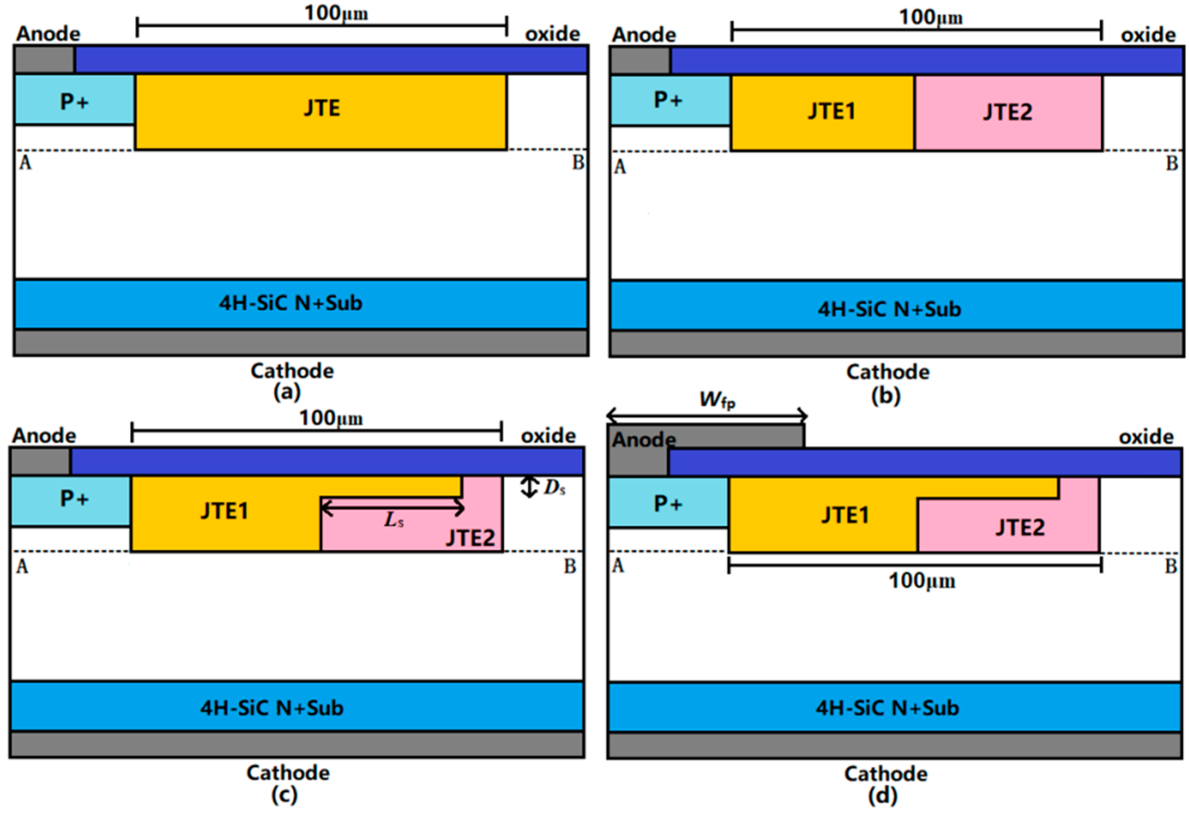
In this section, a 4H-SiC PIN diode with a 30-μm epi-layer doped at 3 × 1015 cm−3 can attain 4000 V from the ideal parallel junction [27]. All termination structures for PIN diodes were investigated using Silvaco TCAD 2-D device simulations (atlas 5.22.1.R, Silvaco Inc., Santa Clara, CA, USA). The breakdown condition was defined as the point at which the calculated impact ionization integral reaches unity [23]. The major models used in simulations include Schokley‒Read‒Hall (SRH), Auger recombination, impact ionization, and incomplete ionization. Cross-sectional views of PIN diodes with three termination structures are shown in Figure 1, including: (a) single-zone JTE (SZ-JTE); (b) double-zone JTE (DZ-JTE); (c) Step-DZ-JTE; (d) Step-DZ-JTE with FP. The feature of Step-DZ-JTE is a step structure, which improves EF distribution by adjusting the depth and length of the step JTE. In addition, Step-DZ-JTE with FP can reduce the amount of EF crowding near the main junction in a low JTE dose by adding an anode FP. In this figure “Ds”, “Ls”, “Wfp” are the depth and length of step JTE1, and the length of the anode FP, respectively. Among these structures, the length of termination region is fixed at 100 µm, where the simulated BV of the JTE starts to saturate. The values of the major optimized parameters of the proposed structure are summarized in Table 1.
2.2. Fabrication Procedure
Figure 2 shows a feasible fabrication procedure for building a step JTE in the Step-DZ-JTE. As shown in Figure 2a, an n- 4H-SiC epitaxial layer is first grown on an n+ 4H-SiC substrate. Then, SiO2 layer as the mask materials are thermally grown on the epitaxial layer and a photoresist is patterned on the mask to form a JTE2 window [28]. Next, multiple aluminum implantations are applied to form the JTE2 region. Then, a graphite cap layer is grown on the surface after removing the mask material to prevent the sublimation and roughening of the surface during the next annealing [28,29]. Next the implantations of the JTE2 are activated by high temperature annealing to activate acceptor impurities and form a box profile, as shown in Figure 2b. In order to form the step distribution of the JTE1, the step mask, as shown in Figure 2c is the key to the formation of the JTE and its shape can be form by the etching process. Similarly, the JTE1 region is formed using ion implantation through the mask and then activation annealing. Finally, the main P+ region is formed using ion implantation with high doses, as shown in Figure 2d. All annealing conditions are implemented at the temperature of 1650 °C under argon ambient with the graphite cap [30]. This process is easier to implement than etching, and it avoids the extra interface charges caused by filling the dielectric after etching.
3. Results
3.1. Simulation Optimization of the DZ-JTE
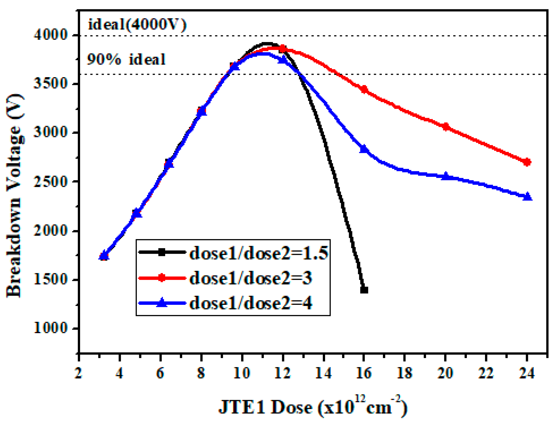
Based on the optimized conventional SZ-JTE, this section discusses the optimization of the DZ-JTE, which mainly involves the length and dose of the double JTE. Figure 3 shows the simulated BV versus the ratio of dose1 in JTE1 to dose2 in JTE2 for DZ-JTE. In the higher JTE1 dose range, the ratio of doses has a significant effect on the BV. The BV increases as the ratio increases, and then drops sharply. There is a reasonable ratio value of doses to avoid a sharp decrease in the BV. As can be seen from the figure, the optimized ratio value of dose1/dose2 is 3.
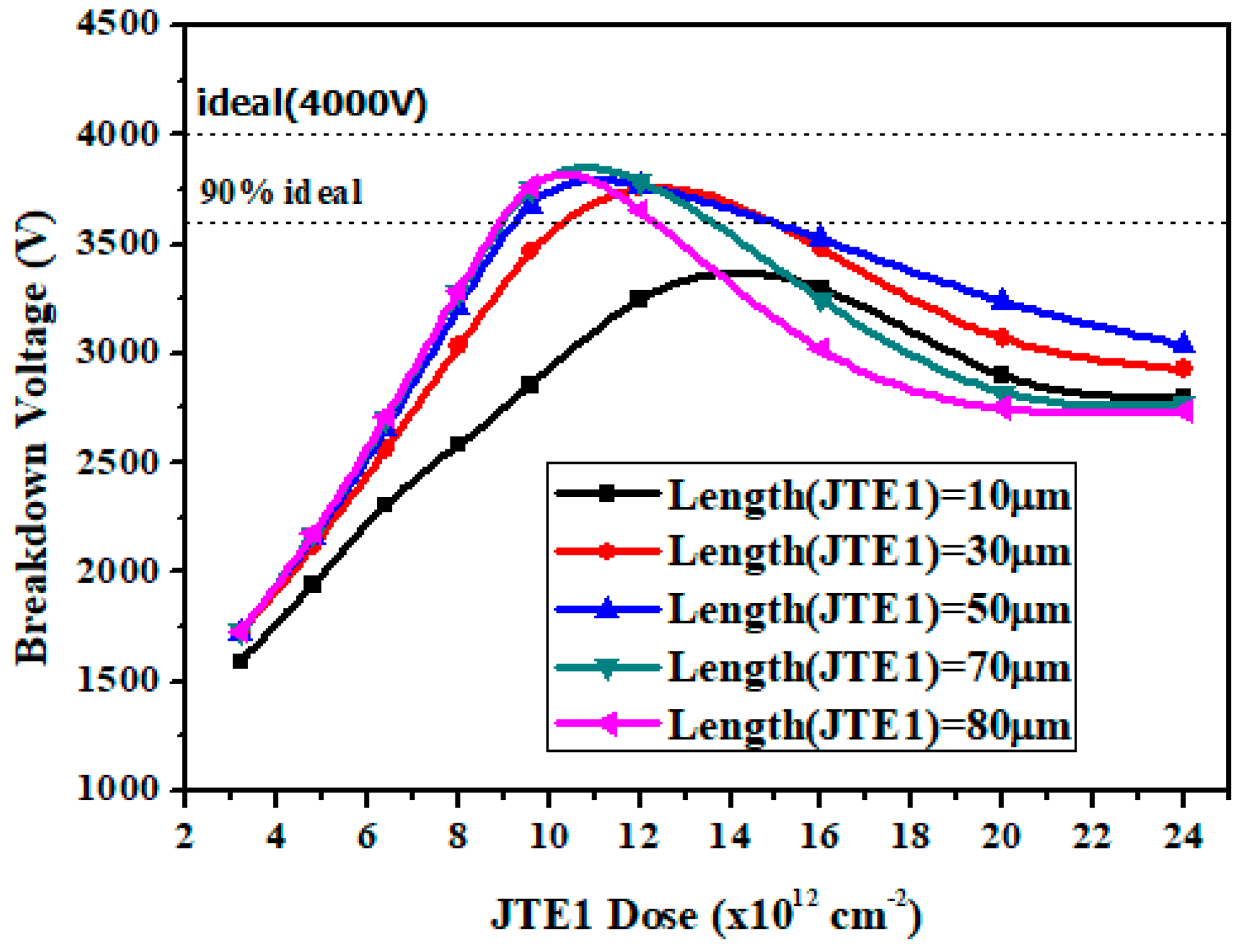
Based on the optimized ratio above, the simulated BV versus JTE1 length for DZ-JTE with different JTE1 dose is shown in Figure 4. We see that JTE1 length has little effect on BV in the lower of JTE1 dose range. This phenomenon is explained by the fact that too low a concentration makes no difference between JTE1 and JTE2. In other JTE1 doses, as JTE1 length increases, the curve gradually rises. When JTE1 length is 50 μm, the curve reaches its highest point. In addition, the curve drops rapidly as JTE1 length exceed 50 μm. This is because, when the JTE1 length is too long, the JTE2 length is shorter and the effect of JTE2 (alleviating the EF of JTE1) is reduced.
3.2. Simulation Optimization of the Step-DZ-JTE with FP
Based on the optimized DZ-JTE, this section optimizes the length and depth of the step JTE1 for the proposed Step-DZ-JTE. Figure 5 shows the simulated BV versus the depth (Ds) and the length (Ls) of step JTE1 for Step-DZ-JTE with FP. As can be seen from Figure 5a, the curve of the BV versus JTE1 dose rises first and then declines as the Ds increases in higher of JTE1 dose range (i.e., >12 × 1012 cm−2). This is because the EF is more concentrated at the end of the step JTE1 with the Ds increases, leading to premature breakdown. When the Ds is 0.3 μm, the Step-DZ-JTE with FP attains the maximum value of the BV, meaning the optimized value of Ds is 0.3 μm. Figure 5b shows the simulated BV versus the length (Ls) of step JTE1 for Step-DZ-JTE. When JTE1 dose is lower than 12 × 1012 cm−2, the Ls has no effect on the relationship between the BV and JTE dose. In the other range of JTE1 dose, the value of 45 μm is a critical value of the Ls. Regardless of whether the Ls is larger or small than the value, the curves of the BV versus JTE1 dose are lower than the curve corresponding to 45 μm. It can be seen from the figure that the longer the Ls is, the faster the curves fall. This phenomenon can be explained by the fact that the longer the Ls is, the higher the carrier concentration is in the step JTE1, resulting in EF crowding at the end of the step JTE1 in the reverse blocking state.
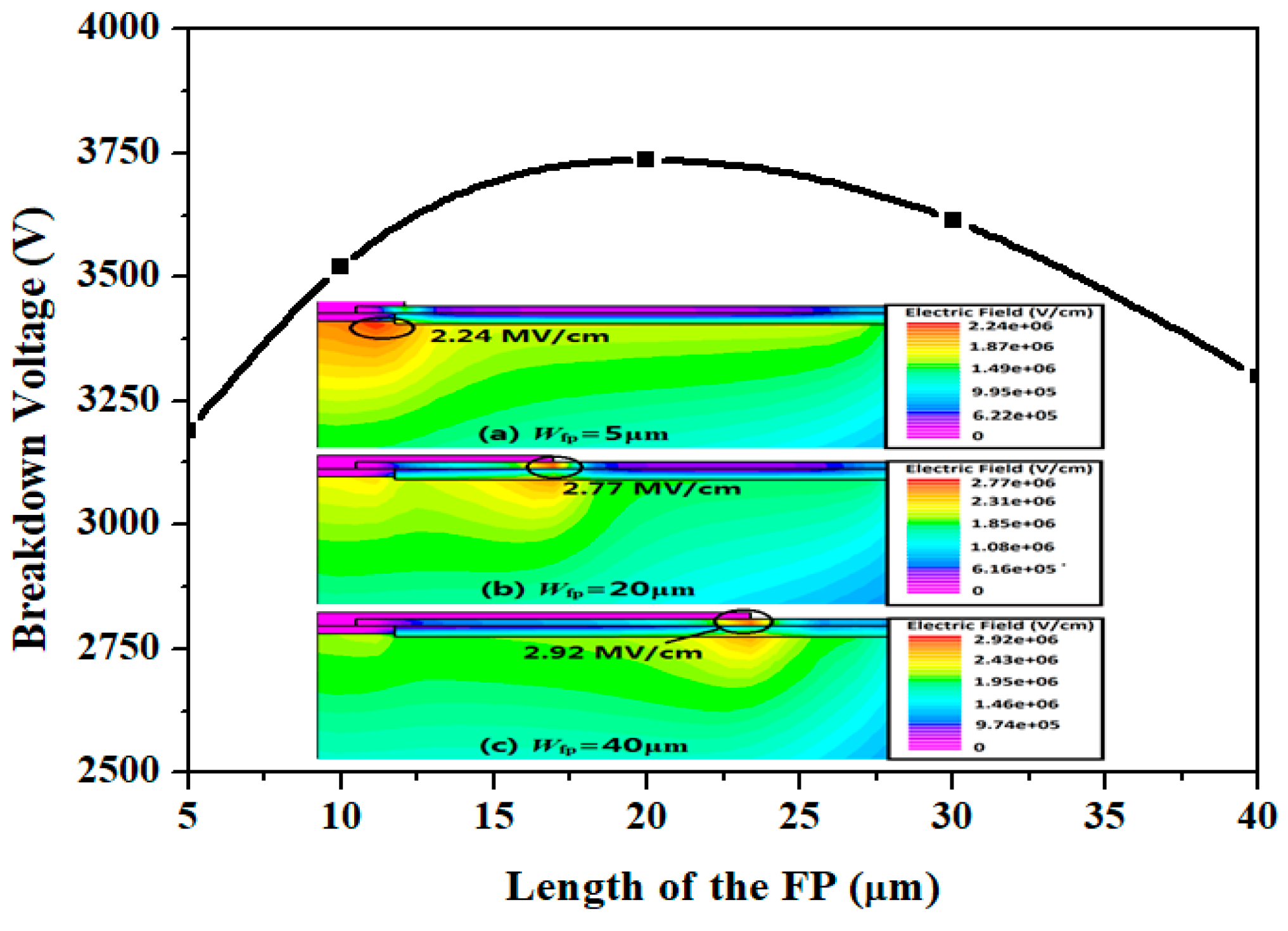
Figure 6 shows the effect of FP on the simulated BV for the Step-DZ-JTE with FP. The maximum BV is obtained when the FP length (Wfp) is 20 μm. The insets of Figure 6 show simulated EF distribution at breakdown with different Wfp. As shown in inset (a), the peak EF occurred near the main junction when the Wfp is less than 20 μm (e.g., 5 μm). As the Wfp increases, the EF crowding near the main can be effectively suppressed by the FP as shown in inset (b). The oxide field is 2.77 MV/cm, shown in inset (b), which is less than the oxide critical field (6 MV/cm in [31]). This means that there is no oxide degradation at breakdown. When the Wfp is more than the optimal length, the location of the peak EF shifts into the periphery of the FP, as shown in inset (c). As can be seen from inset (c), the oxide field (2.92 MV/cm) is also less than 6 MV/cm.
3.3. Compare Electric Field Distribution
The distribution of the electric field under the reverse blocking characteristic can reflect the problem of the conventional terminal structures and the proposed Step-DZ-JTE can be clearly compare with them. Figure 7 compares the simulated EF distribution along the cutline of AB (shown in Figure 1) and on surface of the JTE for SZ-JTE, DZ-JTE, and Step-DZ-JTE with FP at the reverse blocking voltage of 3500 V when JTE1 dose is 2 × 1013 cm−2. Regardless of the distribution of the EF along the bottom of the JTE (Figure 7a) or the distribution of the EF along the JTE surface (Figure 7b), the trend of their curves is generally the same. At this high JTE dose, the peak EF occurred at the end of JTE for the SZ-JTE, resulting in breakdown prematurely. The DZ-JTE can improve the EF at the terminal edge, but a new peak EF appears at the end of the JTE1. Under the effect of step JTE, the Step-DZ-JTE with FP further suppresses the EF crowding at the end of the JTE1. However, the effect of the FP for the Step-DZ-JTE with FP is very small. This is because that concentration of the acceptor carrier is too large at this high JTE dose, so that the effect of the FP absorbing part of the EF is not obvious.
4. Discussion
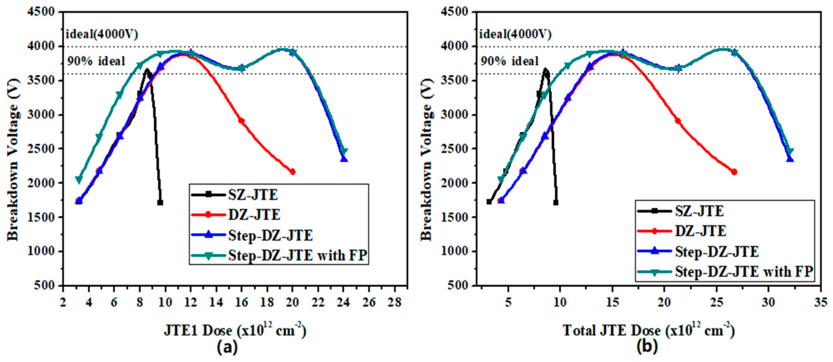
In order to evaluate the performance of the Step-DZ-JTE, it is compared with other termination structures while examining the effects of JTE1 dose and surface charges (SC). First, we discuss the effect JTE dose has on the simulated BV. Figure 8 shows the BV as a function of the JTE1 dose and total JTE dose. As can be seen from Figure 8a, the SZ-JTE shows a very narrow JTE dose tolerance of 0.4 × 1012 cm−2 at 90% of the ideal BV. For the SZ-JTE, the percentage of positive and negative variation allowed to deviate from the optimized dose are +2.2% and −2.2% (positive means tolerance to allow for exceeding the optimized JTE dose; negative means tolerance to allow for less than the optimized JTE dose). By adopting two zones with different doses, the DZ-JTE shows a significant improvement of 4.1 × 1012 cm−2 at 90% of the ideal BV, of which the percentage of positive and negative variation are +17.5% and −17.0% The Step-DZ-JTE, proposed in this paper, is superior to the two termination structures mentioned above. The Step-DZ-JTE has a BV with reduced sensitivity to JTE1 dose and exhibits a wider JTE1 dose tolerance of 12.2 × 1012 cm−2 at 90% of the ideal BV of which the percentage variations are +75% and +18.4%. In the Step-DZ-JTE with FP, the curve coincides with the Step-DZ-JTE at the higher JTE dose. However, at a low JTE1 dose, the Step-DZ-JTE with FP performs better than the Step-DZ-JTE. This is because FP can relieve the EF in the main junction at low JTE1 dose. Thus, the Step-DZ-JTE creates a wide range of JTE1 dose at 90% of the ideal BV with 13.8 × 1012 cm−2, of which the percentage variations are +75% and −35%. In addition, the total JTE dose can be calculated based on the previously optimized ratio value of dose1/dose2. The relationship between the BV and total dose is shown in Figure 8b. Total JTE dose tolerance for 90% of the ideal BV with four terminal structures are listed in Table 2.
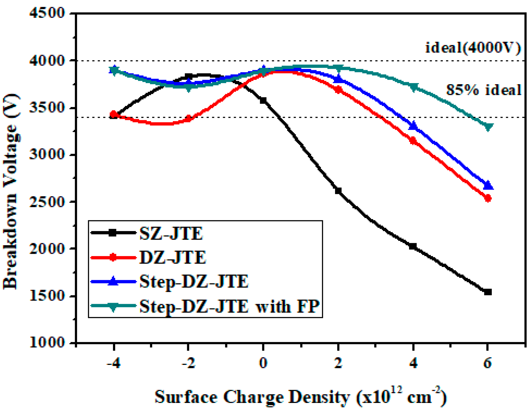
On the other hand, the effect of SC on the BV is investigated since SC will affect the charge distribution and, thus, the EF distribution. In particular, positive SC has a large influence because the positive charges cancel the depleted acceptors in the JTE region. As a result, as shown in Figure 9, the SZ-JTE exhibits a very small tolerance to positive SC and obtains a positive charge density of 0.5 × 1012 cm−2 at 85% of the ideal BV. The DZ-JTE and Step-DZ-JTE show a BV with reduced sensitivity to SC and they obtain a positive charge density of 3.2 × 1012 cm−2 and 3.7 × 1012 cm−2 at 85% of the ideal BV, respectively. However, after adding the FP, the Step-DZ-JTE with FP shows the widest positive charge density of 5.5 × 1012 cm−2. Table 2 summarizes the basic performance of the four different termination structures. Compared with DZ-JTE, the number of p-type ion implantations for the proposed Step-DZ-JTE did not increase, and the performance of the Step-DZ-JTE is greatly improved. Combined with FP technology, the Step-DZ-JTE with FP further reduces the sensitivity of BV to JTE doses and surface charges.
5. Conclusions
A Step-DZ-JTE edge termination scheme is proposed in this paper and the device simulation results show that it has superior terminal performance. A comparison of the simulation results for the SZ-JTE and DZ-JTE shows that the Step-DZ-JTE greatly reduces the sensitivity of the JTE dose and SC. For a 30-µm epi-layer, the Step-DZ-JTE can exhibits a wider JTE dose tolerance of 12.2 × 1012 cm−2 at 90% of the ideal BV and a positive charge density of 3.2 × 1012 cm−2 at 85% of the ideal BV. The Step-DZ-JTE with FP is introduced on the basis of a Step-DZ-JTE by adding an anode FP. The Step-DZ-JTE with FP further improves the effects of JTE dose and SC. Moreover, the Step-DZ-JTE with FP does not require an additional fabrication process. These performance improvements show that the Step-DZ-JTE with FP is a promising edge termination technique for SiC devices.
Author Contributions
Investigation—Y.H., W.W., J.T. and Y.S.; Conceptualization—Y.W.; Software—X.K.
Funding
This work was supported by the National Natural Science Foundation of China (No. 61774052) and the Excellent Youth Foundation of Zhejiang Province of China (No. LR17F040001).
Conflicts of Interest
The authors declare no conflict of interest.
References
- Shenai, K.; Scott, R.S.; Baliga, B.J. Optimum semiconductors for high-power electronics. IEEE Trans. Electron. Devices 1989, 36, 1811–1823. [Google Scholar] [CrossRef]
- Elasser, A.; Chow, T.P. Silicon carbide benefits and advantages for power electronics circuits and systems. Proc. IEEE 2002, 90, 969–986. [Google Scholar] [CrossRef] [Green Version]
- Kimoto, T. Ultrahigh-voltage SiC devices for future power infrastructure. In Proceedings of the 2013 Proceedings of the European Solid-State Device Research Conference, Bucharest, Romania, 16–20 September 2013; pp. 22–29. [Google Scholar] [CrossRef]
- Casady, J.B.; Johnson, R.W. Status of silicon carbide (SiC) as a wide-bandgap semiconductor for high-temperature applications: A review. Solid-State Electron. 1996, 39, 1409–1422. [Google Scholar] [CrossRef]
- Buttay, C.; Raynaud, C.; Morel, H.; Civrac, G.; Locatelli, M.L.; Morel, F. Thermal stability of silicon carbide power diodes. IEEE Trans. Electron. Devices 2012, 59, 761–769. [Google Scholar] [CrossRef]
- Shankar, B.; Gupta, S.K.; Taube, W.R.; Akhtar, J. High-k dielectrics based field plate edge termination engineering in 4H-SiC Schottky diode. Int. J. Electron. 2016, 103, 2064–2074. [Google Scholar] [CrossRef]
- Tarplee, M.C.; Madangarli, V.P.; Zhang, Q.; Sudarshan, T.S. Design rules for field plate edge termination in SiC Schottky diodes. IEEE Trans. Electron. Devices 2001, 48, 2659–2664. [Google Scholar] [CrossRef]
- Brunt, E.V.; Cheng, L.; O’Loughlin, M.; Capell, C. 22 kV, 1 cm2, 4H-SiC n-IGBTs with improved conductivity modulation. In Proceedings of the International Symposium on Power Semiconductor Devices & Ic’s, Waikoloa, HI, USA, 15–19 June 2014; pp. 358–361. [Google Scholar] [CrossRef]
- Villamor-Baliarda, A.; Vanmeerbeek, P.; Roig, J.; Moens, P. Electric field unbalance for robust floating ring termination. Microelectron. Reliab. 2011, 51, 1959–1963. [Google Scholar] [CrossRef]
- Sung, W.; Baliga, B.J. A Near Ideal Edge Termination Technique for 4500V 4H-SiC Devices: The Hybrid Junction Termination Extension (Hybrid-JTE). IEEE Electron. Device Lett. 2016, 37, 1609–1612. [Google Scholar] [CrossRef]
- Mahajan, A.; Skromme, B.J. Design and optimization of junction termination extension (JTE) for 4H SiC high voltage Schottky diodes. Solid State Electron. 2005, 49, 945–955. [Google Scholar] [CrossRef]
- Okayama, T.; Arthur, S.D.; Rao, R.R.; Kishore, K.; Rao, M.V. Stability and 2-D Simulation Studies of Avalanche Breakdown in 4H-SiC DMOSFETS with JTE. IEEE Trans. Electron Devices. 2008, 55, 489–494. [Google Scholar] [CrossRef]
- Zhang, F.; Xing-Hua, F.U. Simulation study on 4H-SiC Schottky diode with JTE structure. In Proceedings of the 2014 16th European Conference on Power Electronics and Applications, Lappeenranta, Finland, 26–28 August 2012. [Google Scholar]
- Feng, G.; Suda, J.; Kimoto, T. Space-Modulated Junction Termination Extension for Ultrahigh-Voltage p-i-n Diodes in 4H-SiC. IEEE Trans. Electron. Devices 2012, 59, 414–418. [Google Scholar] [CrossRef]
- Deng, X.; Li, L.; Wu, J.; Li, C.; Chen, W. A Multiple-Ring-Modulated JTE Technique for 4H-SiC Power Device with Improved JTE-Dose Window. IEEE Trans. Electron. Devices 2017, 64, 5042–5047. [Google Scholar] [CrossRef]
- Perez, R.; Tournier, D.; Perez-Tomas, A.; Godignon, P.; Mestres, N. Planar edge termination design and technology considerations for 1.7-kV 4H-SiC PiN diodes. IEEE Trans. Electron. Devices 2005, 52, 2309–2316. [Google Scholar] [CrossRef]
- Perez, R.; Mestres, N.; Tournier, D. A highly effective edge termination design for SiC planar high power devices. Mater. Sci. Forum 2014, 457–460, 1253–1256. [Google Scholar] [CrossRef]
- Zhang, F.; Li, X. Research on high-voltage 4H-SiC P-i-N diode with planar edge junction termination techniques. Chin. Phys. B 2011, 20, 366–371. [Google Scholar] [CrossRef]
- Huang, R.; Tao, Y.; Wang, L.; Chen, G.; Bai, S. Development of g10kv 4H-SiC SBD junction extension termination. In Proceedings of the International Conference on Advanced Electronic Science and Technology, Shenzhen, China, 19–21 August 2016. [Google Scholar] [CrossRef]
- Sheridan, D.C.; Niu, G.; Cressler, J.D. Design of single and multiple zone junction termination extension structures for SiC power devices. Solid-State Electron. 2001, 45, 1659–1664. [Google Scholar] [CrossRef]
- Sung, W.; Brunt, E.V.; Baliga, B.J.; Huang, A.Q. A new edge termination technique for high-voltage devices in 4H-SiC–multiple-floating-zone junction termination extension. IEEE Electron. Device Lett. 2011, 32, 880–882. [Google Scholar] [CrossRef]
- Ghandi, R.; Buono, B.; Domeij, M.; Zetterling, C.M. High-Voltage 4H-SiC PiN Diodes with Etched Junction Termination Extension. IEEE Electron. Device Lett. 2009, 30, 1170–1172. [Google Scholar] [CrossRef]
- Pâques, G.; Dheilly, N.; Planson, D.; Scharnholz, S. Graded Etched Junction Termination for SiC Thyristors. Mater. Sci. Forum 2011, 679–680, 457–460. [Google Scholar] [CrossRef]
- Huang, C.F.; Hsu, H.C.; Chu, K.W.; Lee, L.H.; Tsai, M.J. Counter-Doped JTE, an Edge Termination for HV SiC Devices with Increased Tolerance to the Surface Charge. IEEE Trans. Electron. Devices 2015, 62, 354–358. [Google Scholar] [CrossRef]
- Kaji, N.; Niwa, H.; Suda, J.; Kimoto, T. Ultrahigh-Voltage SiC p-i-n Diodes with Improved Forward Characteristics. IEEE Trans. Electron. Devices 2015, 62, 374–381. [Google Scholar] [CrossRef]
- Deng, X.; Chen, X.; Li, C.; Shen, H.; Zhang, J. Numerical and experimental study of the mesa configuration in high-voltage 4H–SiC PiN rectifiers. Chin. Phys. B 2016, 25, 087201. [Google Scholar] [CrossRef]
- Baliga, B.J. Fundamentals of Power Semiconductor Devices; Springer: New York, NY, USA, 2008; Chapter 3; pp. 91–155. [Google Scholar] [CrossRef]
- Kim, S.C.; Bahng, W.; Kang, I.H. Fabrication characteristics of 1.2 kV SiC JBS diode. In Proceedings of the International Conference on Microelectronics, Nis, Serbia & Montenegro, 11–14 May 2008; pp. 181–184. [Google Scholar]
- Hiyoshi, T.; Hori, T.; Suda, J. Simulation and Experimental Study on the Junction Termination Structure for High-Voltage 4H-SiC PiN Diodes. IEEE Trans. Electron. Devices 2008, 55, 1841–1846. [Google Scholar] [CrossRef] [Green Version]
- Wang, C.; Yuan, H.; Song, Q. Fabrication of 3.1 kV/10 A 4H-SiC Junction Barrier Schottky Diodes. In Proceedings of the 2015 IEEE 11th International Conference on ASIC (ASICON), Chengdu, China, 3–6 November 2015; pp. 1–3. [Google Scholar]
- Lee, C.Y.; Yen, C.T.; Chu, K.W.; Chen, Y.S. A novel 4H-SiC Trench MOS Barrier Schottky rectifier fabricated by a two-mask process. In Proceedings of the International Symposium on Power Semiconductor Devices and ICS, Kanazawa, Japan, 26–30 May 2013; pp. 171–174. [Google Scholar] [CrossRef]
Figure 1.
Schematic structures of (a) single-zone junction termination extension (SZ-JTE); (b) double-zone JTE (DZ-JTE); (c) Step-DZ-JTE; (d) Step-DZ-JTE with field plate (FP). The n- epi-layer is 30-µm thick and 2 × 1015 cm−3 doped.
Figure 1.
Schematic structures of (a) single-zone junction termination extension (SZ-JTE); (b) double-zone JTE (DZ-JTE); (c) Step-DZ-JTE; (d) Step-DZ-JTE with field plate (FP). The n- epi-layer is 30-µm thick and 2 × 1015 cm−3 doped.

Figure 2.
Fabrication procedure of making step JTE in the Step-DZ-JTE. (a) Base layers. (b) JTE2 region formed by ion implantation. (c) JTE1 region fromed by ion implantation with the specific mask. (d) Main junction P+ formation.
Figure 2.
Fabrication procedure of making step JTE in the Step-DZ-JTE. (a) Base layers. (b) JTE2 region formed by ion implantation. (c) JTE1 region fromed by ion implantation with the specific mask. (d) Main junction P+ formation.
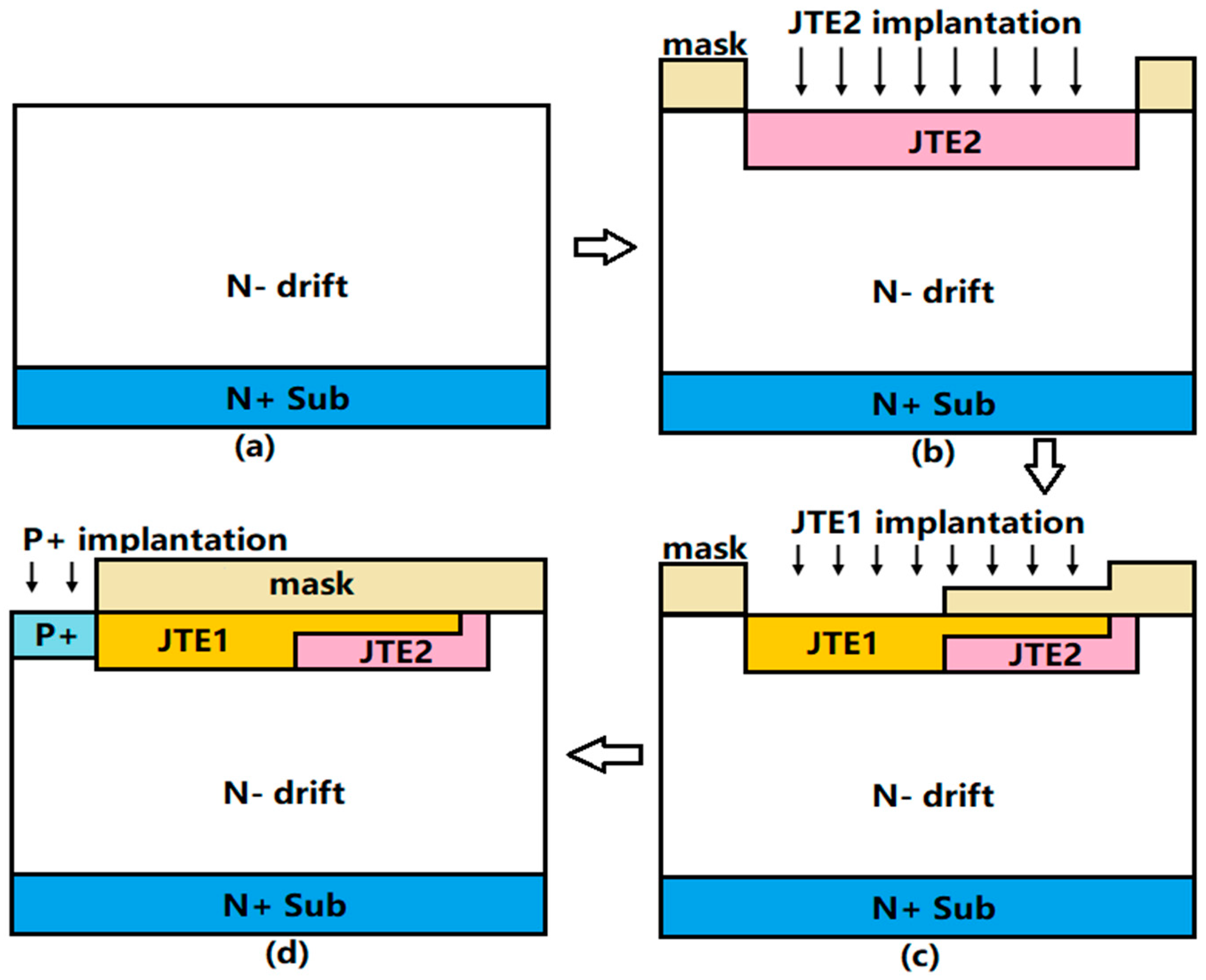
Figure 3.
Simulated breakdown voltage (BV) versus ratio of the doses with different doses for the DZ-JTE optimization.
Figure 3.
Simulated breakdown voltage (BV) versus ratio of the doses with different doses for the DZ-JTE optimization.

Figure 4.
Simulated BV versus JTE1 length with different doses for the DZ-JTE optimization.

Figure 5.
Simulated BV versus (a) the depth (Ds) and (b) the length (Ls) of the Step JTE for Step-DZ-JTE optimization.
Figure 5.
Simulated BV versus (a) the depth (Ds) and (b) the length (Ls) of the Step JTE for Step-DZ-JTE optimization.
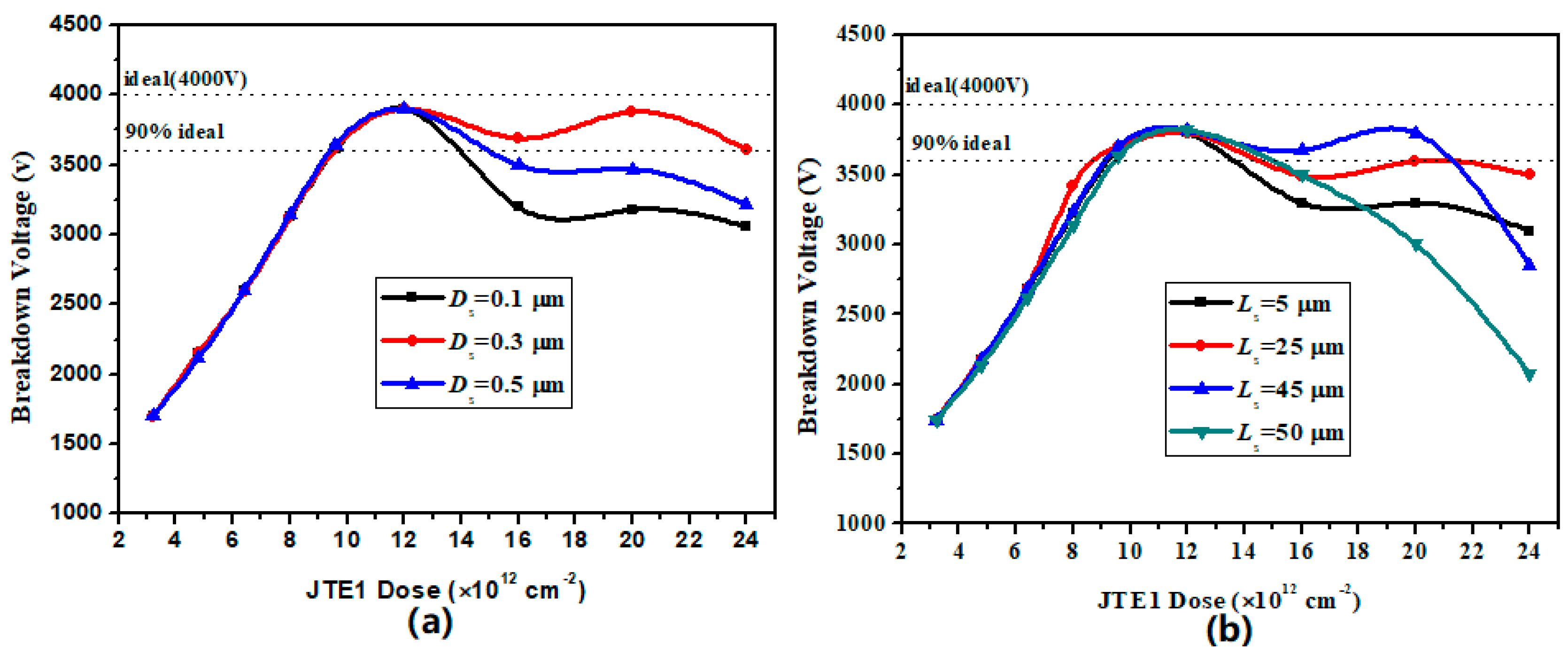
Figure 6.
Simulated BV versus FP length (Wfp) for the Step-DZ-JTE with FP optimization.

Figure 7.
Simulated electric field distribution at OFF-state breakdown (a) along the cutline of AB and (b) on the surface for SZ-JTE, DZ-JTE, Step-DZ-JTE with FP (dose1/dose2 = 3, and JTE1 dose = 2 × 1013 cm−2).
Figure 7.
Simulated electric field distribution at OFF-state breakdown (a) along the cutline of AB and (b) on the surface for SZ-JTE, DZ-JTE, Step-DZ-JTE with FP (dose1/dose2 = 3, and JTE1 dose = 2 × 1013 cm−2).
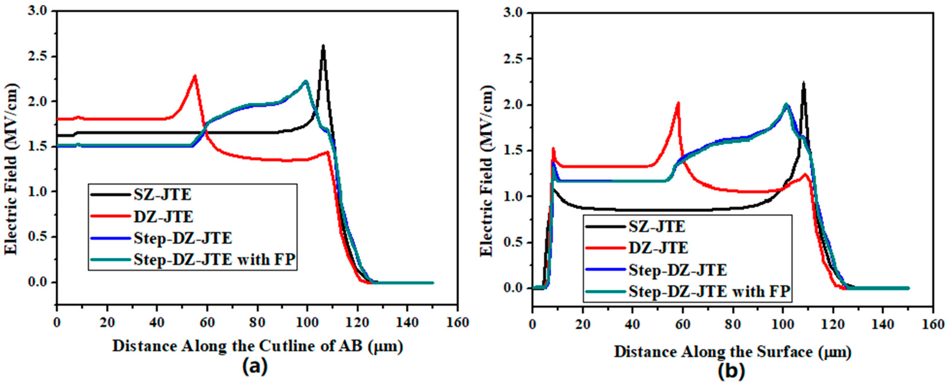
Figure 8.
Simulated BV versus (a) JTE1 dose and (b) total JTE dose for SZ-JTE, DZ-JTE, Step-DZ-JTE without FP, and Step-DZ-JTE with FP.
Figure 8.
Simulated BV versus (a) JTE1 dose and (b) total JTE dose for SZ-JTE, DZ-JTE, Step-DZ-JTE without FP, and Step-DZ-JTE with FP.

Figure 9.
Simulated BV versus surface charges for SZ-JTE, DZ-JTE, Step-DZ-JTE without FP, and Step-DZ-JTE with FP.
Figure 9.
Simulated BV versus surface charges for SZ-JTE, DZ-JTE, Step-DZ-JTE without FP, and Step-DZ-JTE with FP.

Table 1.
Major optimized parameters of the proposed structure.
| Parameter | Value |
|---|---|
| P+ anode junction depth | 0.6 μm |
| Junction termination extension (JTE) junction depth | 0.8 μm |
| Depth of the step JTE (Ds) | 0.3 μm |
| Length of the step JTE (Ls) | 45 μm |
| Length of the anode FP (Wfp) | 20 μm |
| Thickness of drift | 30 μm |
| n- drift dopant concentration (ND) | 3.0 × 1015 cm−3 |
| p+ anode dopant concentration (NA) | 1.0 × 1019 cm−3 |
Table 2.
Basic properties of different JTEs.
| Structures | SZ-JTE | DZ-JTE | Step-DZ-JTE | Step-DZ-JTE with FP |
|---|---|---|---|---|
| JTE total length (μm) | 100 | 100 | 100 | 100 |
| Number of p-type implant | 1 | 2 | 2 | 2 |
| JTE1 dose tolerance for 90% BV (× 1012 cm−2) | 0.4 | 4.1 | 12.2 | 13.8 |
| Total JTE dose tolerance for 90% BV ((× 1012 cm−2) | 0.4 | 5.6 | 16.3 | 18.4 |
| The percentage of positive and negative variation | (+2.2%, −2.2%) | (+17.5%, −17.0%) | (+75%, −18.4%) | (+75%, −35%) |
| Max. positive SC density for 85% BV (× 1012 cm−2) | 0.5 | 3.2 | 3.7 | 5.5 |
© 2018 by the authors. Licensee MDPI, Basel, Switzerland. This article is an open access article distributed under the terms and conditions of the Creative Commons Attribution (CC BY) license (http://creativecommons.org/licenses/by/4.0/).
Share and Cite
MDPI and ACS Style
Huang, Y.; Wang, Y.; Kuang, X.; Wang, W.; Tang, J.; Sun, Y. Step-Double-Zone-JTE for SiC Devices with Increased Tolerance to JTE Dose and Surface Charges. Micromachines 2018, 9, 610. https://doi.org/10.3390/mi9120610
AMA Style
Huang Y, Wang Y, Kuang X, Wang W, Tang J, Sun Y. Step-Double-Zone-JTE for SiC Devices with Increased Tolerance to JTE Dose and Surface Charges. Micromachines. 2018; 9(12):610. https://doi.org/10.3390/mi9120610
Chicago/Turabian StyleHuang, Yifei, Ying Wang, Xiaofei Kuang, Wenju Wang, Jianxiang Tang, and Youlei Sun. 2018. "Step-Double-Zone-JTE for SiC Devices with Increased Tolerance to JTE Dose and Surface Charges" Micromachines 9, no. 12: 610. https://doi.org/10.3390/mi9120610
Note that from the first issue of 2016, this journal uses article numbers instead of page numbers. See further details here.