Three-Dimensional Fractal Geometry for Gas Permeation in Microchannels

 , ,
, ,
Abstract
:1. Introduction
2. Materials and Methods
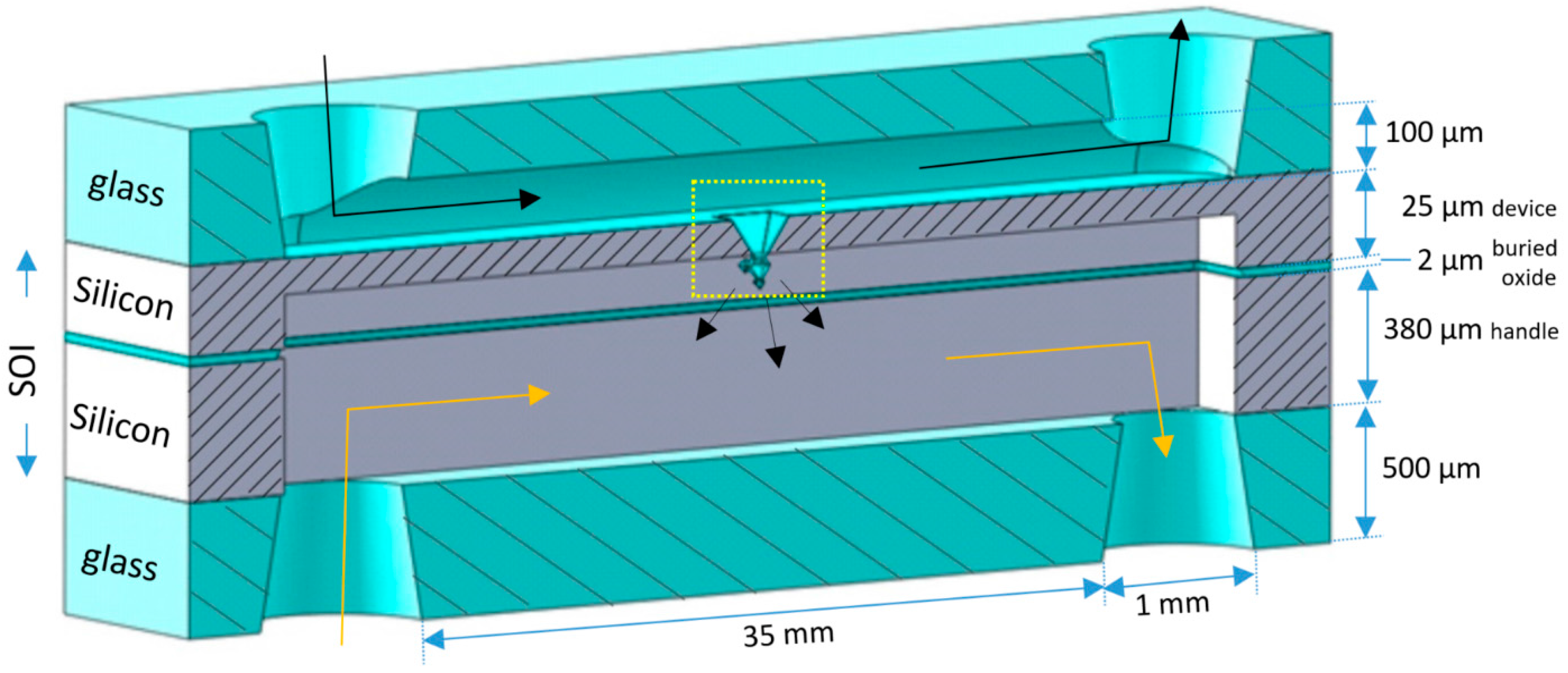
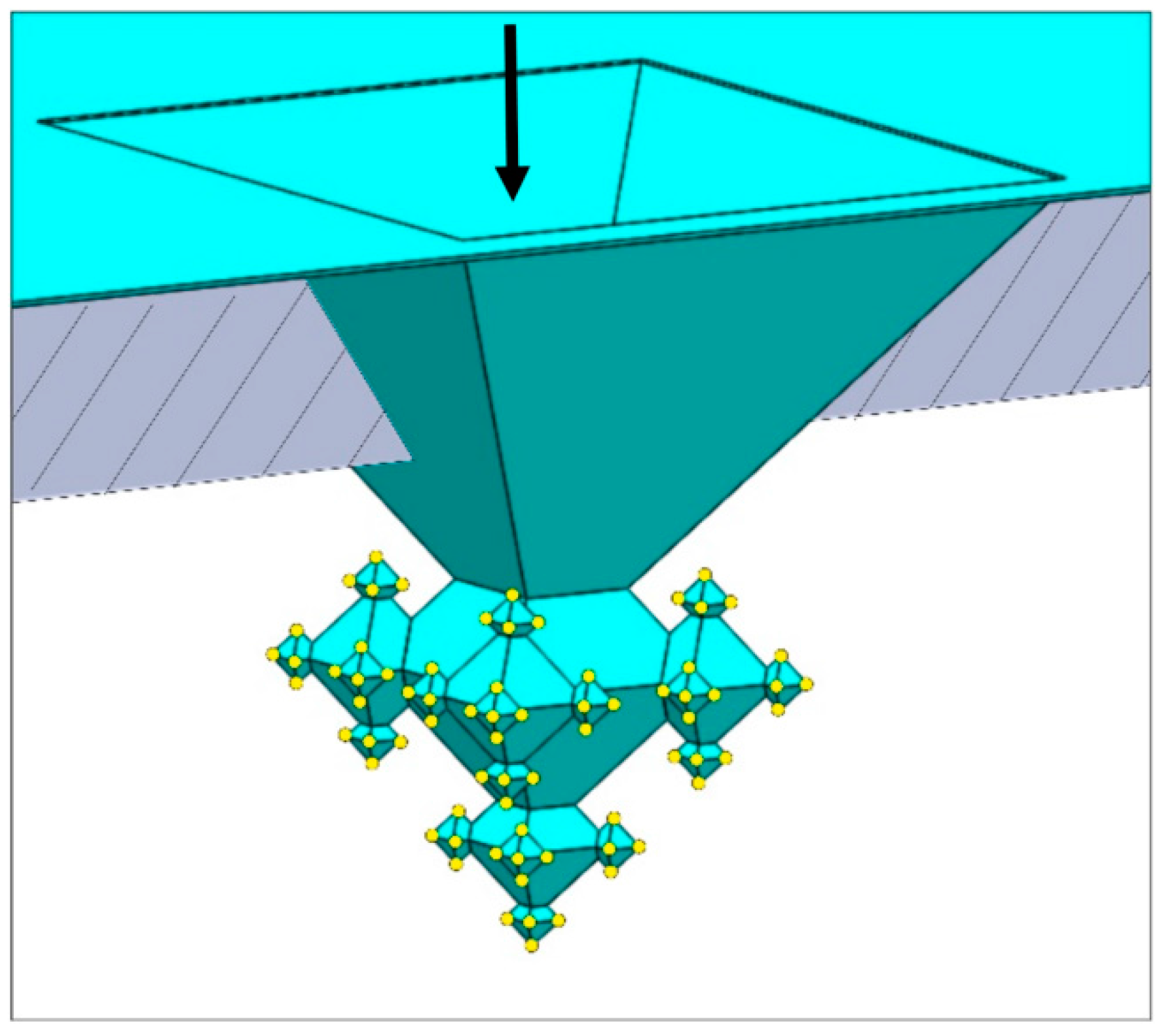
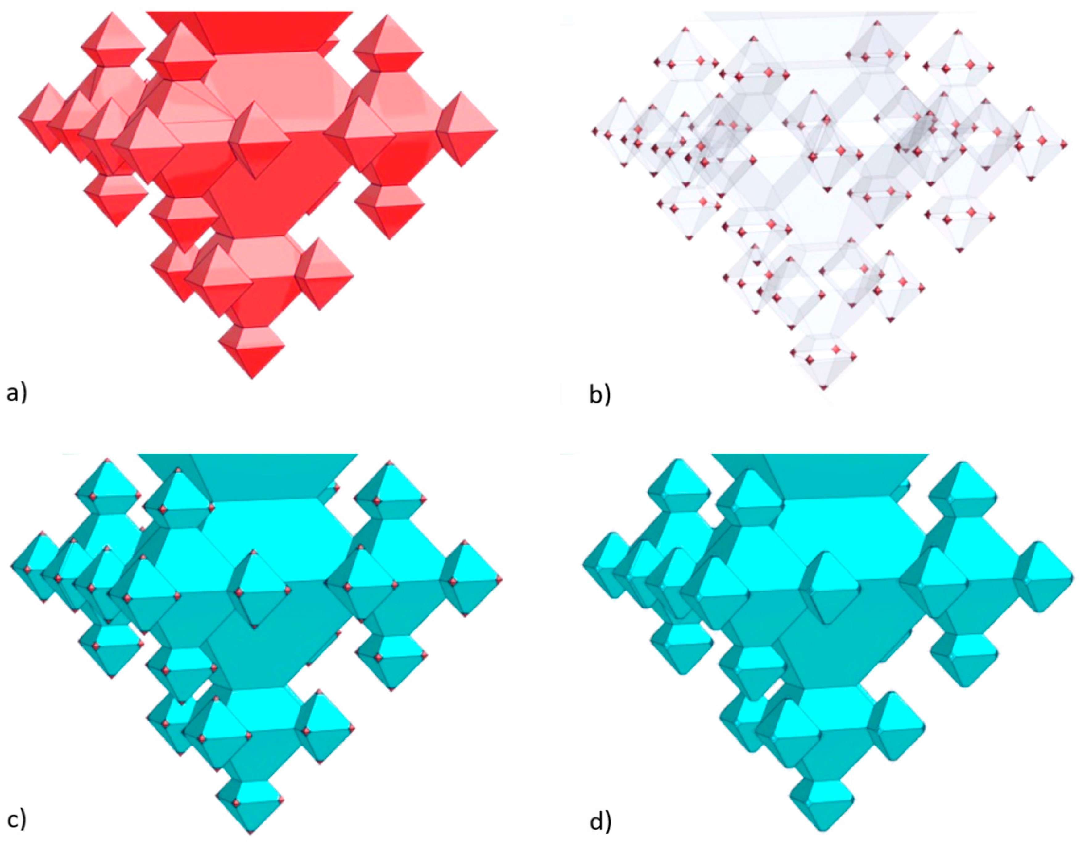
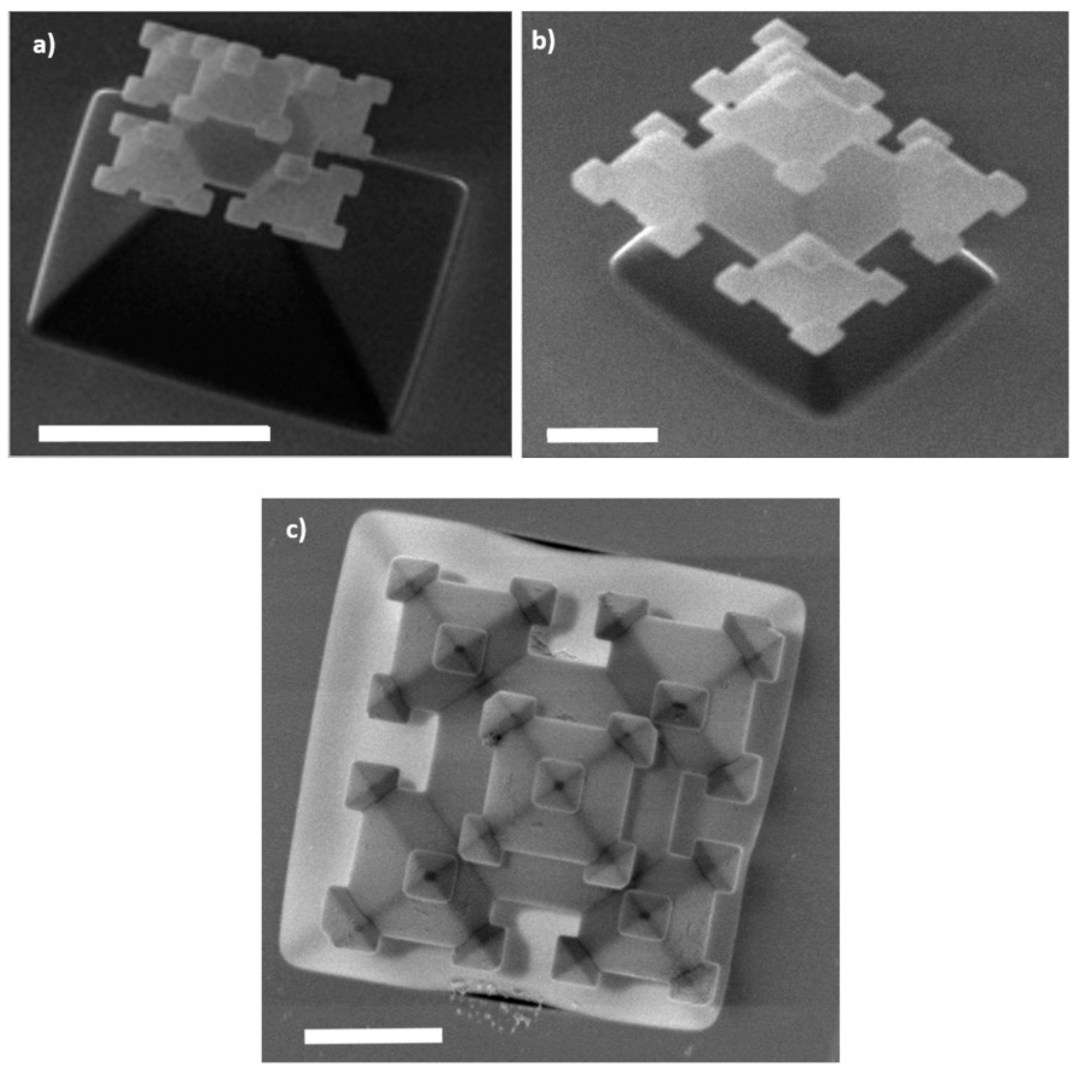
2.1. Integration of Fractals in Microchannels
- In the first step a ca. 163-nm thick SiO2 layer is deposited (dry oxidation, 95 min at 1100 °C), which is isotropically etched in 1% HF for 20.5 min upon which only in the corners of the inverted pyramids the underlying silicon are accessible (i.e., the (100) and (111) Si planes remain covered with SiO2 after this etch time). Then, 1st-generation octahedral structures are etched in silicon with tetramethylammonium hydroxide (TMAH; 25 wt %, 70 °C, 126 min). After TMAH etching the SiO2 layer is removed with 50% HF (18 s), followed by ozone/steam cleaning of the substrate.
- In the second step, again, dry oxidation is used (95 min at 1100 °C), yielding a layer thickness of ca. 159 nm. Similar to the first step, this SiO2 film is isotropically thinned down in 1% HF (19.5 min), followed by anisotropic etching of silicon to create the 2nd-generation octahedral features (TMAH; 25 wt %, 70 °C, 65 min). Immersion of the SOI substrate in 50% HF (18 s) is carried out to remove the SiO2 mask, followed by ozone/steam cleaning to prepare the substrate for the next process step.
- The third step also starts with dry oxidation (95 min at 1100 °C), giving a layer of ca. 160 nm, that is isotropically etched in 1% HF (20 min). The patterned film serves as selective mask during TMAH etching of silicon (25 wt %, 70 °C, 37 min) during which the 3rd-generation octahedrals are formed. Afterwards, the SiO2 film is stripped (50% HF, 15 s) and ozone/steam cleaning is performed.
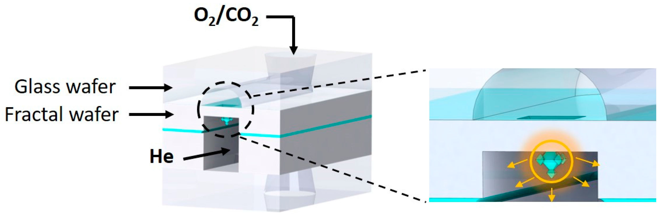
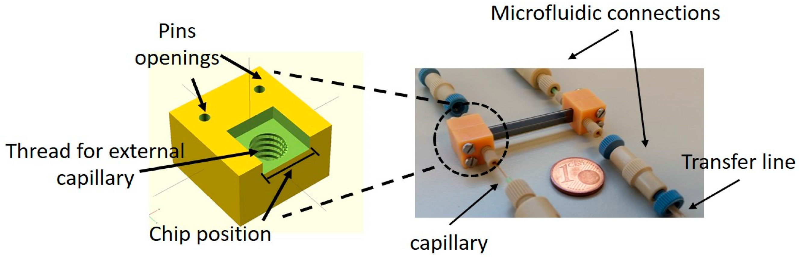
2.2. Chip Design and Assembly
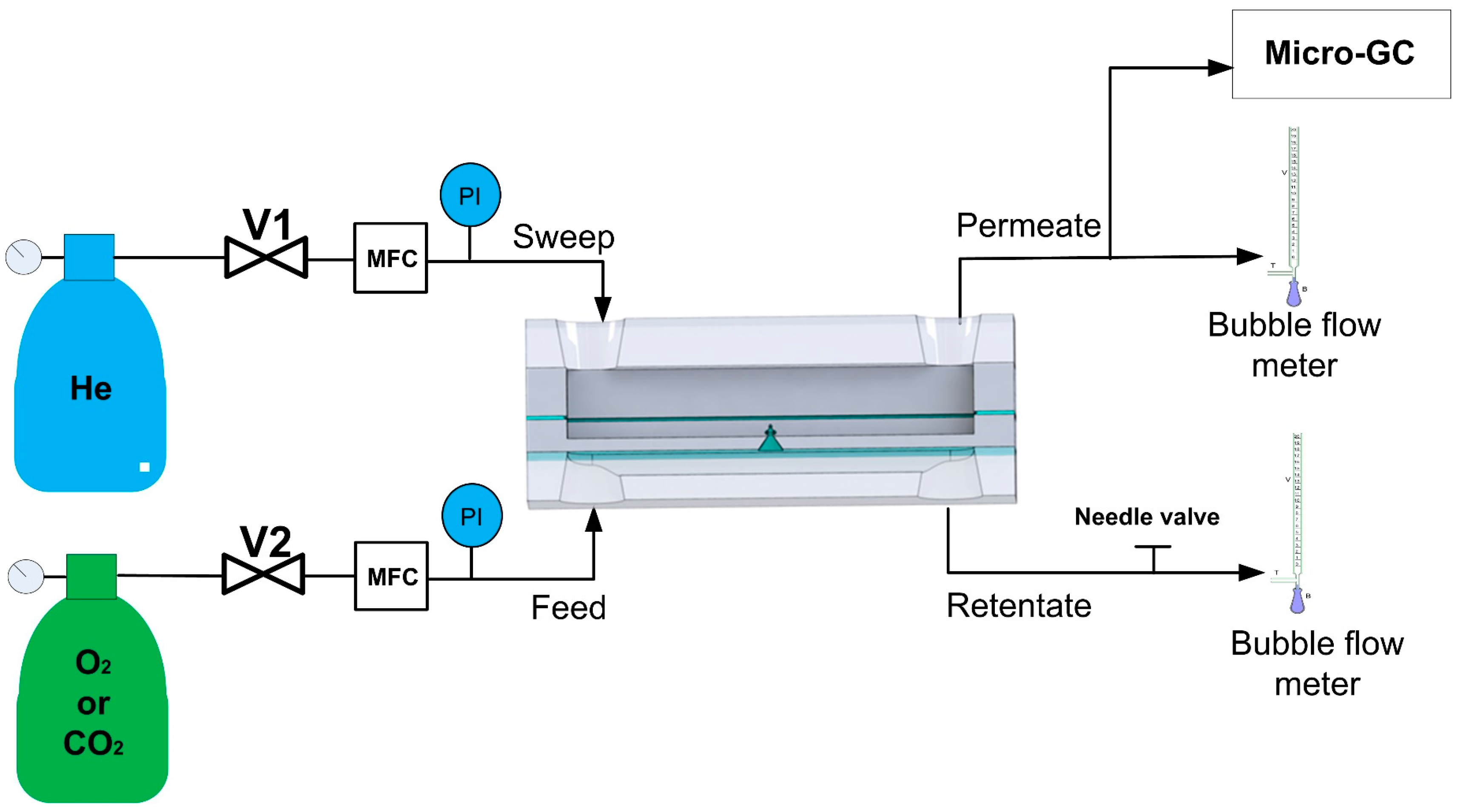
2.3. Gas Permeation Measurements
3. Results and Discussion
4. Conclusions
Acknowledgments
Author Contributions
Conflicts of Interest
References
- Chen, X.; Shen, J. Review of membranes in microfluidics. J. Chem. Technol. Biotechnol. 2017, 92, 271–282. [Google Scholar] [CrossRef]
- De Jong, J.; Lammertink, R.G.H.; Wessling, M. Membranes and microfluidics: A review. Lab Chip Miniat. Chem. Biol. 2006, 6, 1125–1139. [Google Scholar] [CrossRef] [PubMed]
- Ren, X.; Lu, H.; Zhou, J.G.; Chong, P.L.-G.; Yuan, W.; Noh, M. Porous Polydimethylsiloxane as a Gas-Liquid Interface for Microfluidic Applications. J. Microelectromech. Syst. 2017, 26, 120–126. [Google Scholar] [CrossRef]
- Houston, K.S.; Weinkauf, D.H.; Stewart, F.F. Gas transport characteristics of plasma treated poly(dimethylsiloxane) and polyphosphazene membrane materials. J. Membr. Sci. 2002, 205, 103–112. [Google Scholar] [CrossRef]
- Burouni, N.; Berenschot, E.; Elwenspoek, M.; Sarajlic, E.; Leussink, P.; Jansen, H.; Tas, N. Wafer-scale fabrication of nanoapertures using corner lithography. Nanotechnology 2013, 24. [Google Scholar] [CrossRef] [PubMed]
- Berenschot, E.J.W.; Jansen, H.V.; Tas, N.R. Fabrication of 3D fractal structures using nanoscale anisotropic etching of single crystalline silicon. J. Micromech. Microeng. 2013, 23. [Google Scholar] [CrossRef]
- Berenschot, J.W.; Tiggelaar, R.M.; Geerlings, J.; Gardeniers, J.G.E.; Tas, N.R.; Malankowska, M.; Pina, M.P.; Mallada, R. 3D-fractal engineering based on oxide-only corner lithography. in Symposium on Design, Test, Integration and Packaging of MEMS/MOEMS. In Proceedings of the DTIP 2016, 2016 Symposium on Design, Test, Integration and Packaging of MEMS/MOEMS (DTIP), Budapest, Hungary, 30 May–2 June 2016. [Google Scholar]
- Costantini, F.; Benetti, E.M.; Tiggelaar, R.M.; Gardeniers, H.J.; Reinhoudt, D.N.; Huskens, J.; Vancso, G.J.; Verboom, W. A brush-gel/metal-nanoparticle hybrid film as an efficient supported catalyst in glass microreactors. Chem. A Eur. J. 2010, 16, 12406–12411. [Google Scholar] [CrossRef] [PubMed]
- Wensink, H.; Jansen, H.V.; Berenschot, J.W.; Elwenspoek, M.C. Mask materials for powder blasting. J. Micromech. Microeng. 2000, 10, 175–180. [Google Scholar] [CrossRef]
- Veenstra, T.T.; Berenschot, J.W.; Gardeniers, J.G.E.; Sanders, R.G.P.; Elwenspoek, M.C.; van den Berg, A. Use of Selective Anodic Bonding to Create Micropump Chambers with Virtually No Dead Volume. J. Electrochem. Soc. 2001, 148, G68–G72. [Google Scholar] [CrossRef]
- Iczkowski, R.P.; Margrave, J.L.; Robinson, S.M. Effusion of gases through conical orifices. J. Phys. Chem. 1963, 62, 229–233. [Google Scholar] [CrossRef]
- Unnikrishnan, S.; Jansen, H.V.; Falke, F.H.; Tas, N.R.; Van Wolferen, H.A.; De Boer, M.J.; Sanders, R.G.; Elwenspoek, M.C. Transition flow through an ultra-thin nanosieve. Nanotechnology 2009, 20, 305304. [Google Scholar] [CrossRef] [PubMed]
- Keizer, K.; Uhlhorn, R.J.R.; van vuren, R.J.; Burggraaf, A.J. Gas separation mechanisms in microporous modified γ-Al2O3 membranes. J. Membr. Sci. 1988, 39, 285–300. [Google Scholar] [CrossRef]
- Gómez-Goñi, J.; Lobo, P.J. Comparison between Monte Carlo and analytical calculation of the conductance of cylindrical and conical tubes. J. Vac. Sci. Technol. A Vac. Surf. Films 2003, 21, 1452–1457. [Google Scholar] [CrossRef]
- Zhang, X.; Lai, E.S.M.; Martin-Aranda, R.; Yeung, K.L. An investigation of Knoevenagel condensation reaction in microreactors using a new zeolite catalyst. Appl. Catal. A Gen. 2004, 261, 109–118. [Google Scholar] [CrossRef]


| Chip 1 | Chip 2 | |
|---|---|---|
| Channel width (μm) | 500 | 300 |
| Number open fractal structures | 244 | 308 |
| Si membrane area, A (m2) | 1.75 × 10⁻⁵ | 1.05 × 10⁻⁵ |
| Porosity, ε | 1.37 × 10⁻⁵ | 2.88 × 10⁻⁵ |
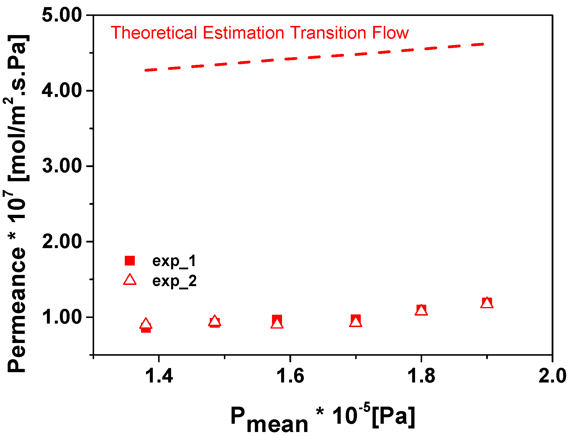
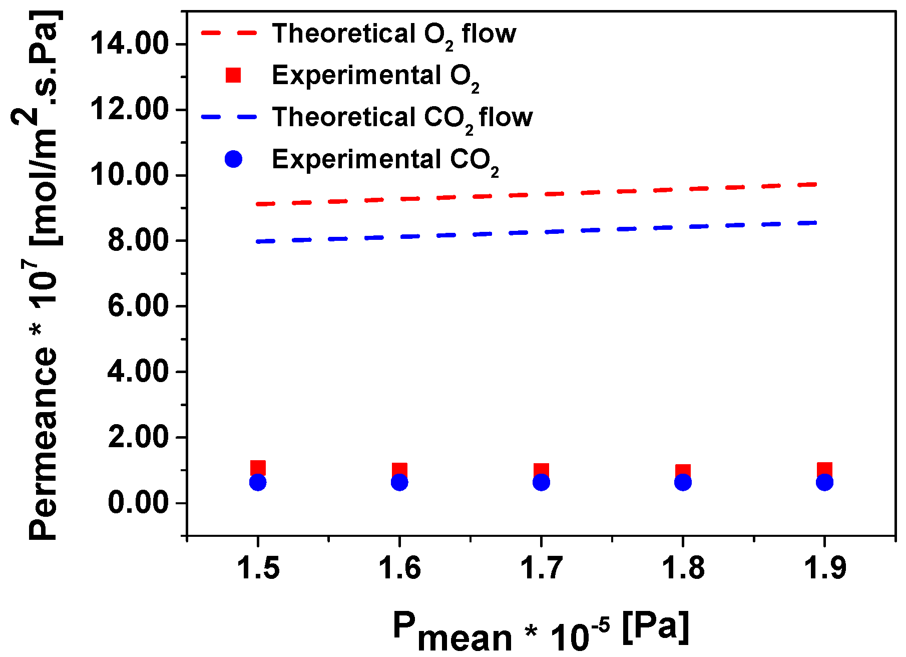
| Pmean·10−5 [Pa] | PO2 [mol/m2·s·Pa] | Equivalent PDMS Thickness [μm] | PCO2 [mol/m2·s·Pa] | Equivalent PDMS Thickness [μm] | |
|---|---|---|---|---|---|
| Chip 1 | Chip 2 | O2 | Chip 2 | CO2 | |
| 1.38 | 8.79 × 10⁻⁸ | 1.02 × 10⁻⁷ | 1.12 | 6.48 × 10⁻⁸ | 4.1 |
| 1.48 | 9.31 × 10⁻⁸ | 1.06 × 10⁻⁷ | 1.07 | 6.31 × 10⁻⁸ | 4.2 |
| 1.58 | 9.34 × 10⁻⁸ | 9.88 × 10⁻⁸ | 1.09 | 6.10 × 10⁻⁸ | 4.3 |
| 1.7 | 9.48 × 10⁻⁸ | 9.85 × 10⁻⁸ | 1.08 | 6.46 × 10⁻⁸ | 4.1 |
| 1.8 | 1.08 × 10⁻⁷ | 9.46 × 10⁻⁸ | 1.00 | 6.26 × 10⁻⁸ | 4.2 |
| 1.9 | 1.18 × 10⁻⁷ | 1.01 × 10⁻⁷ | 0.93 | 5.96 × 10⁻⁸ | 4.4 |
© 2018 by the authors. Licensee MDPI, Basel, Switzerland. This article is an open access article distributed under the terms and conditions of the Creative Commons Attribution (CC BY) license (http://creativecommons.org/licenses/by/4.0/).
Share and Cite
Malankowska, M.; Schlautmann, S.; Berenschot, E.J.W.; Tiggelaar, R.M.; Pina, M.P.; Mallada, R.; Tas, N.R.; Gardeniers, H. Three-Dimensional Fractal Geometry for Gas Permeation in Microchannels. Micromachines 2018, 9, 45. https://doi.org/10.3390/mi9020045
Malankowska M, Schlautmann S, Berenschot EJW, Tiggelaar RM, Pina MP, Mallada R, Tas NR, Gardeniers H. Three-Dimensional Fractal Geometry for Gas Permeation in Microchannels. Micromachines. 2018; 9(2):45. https://doi.org/10.3390/mi9020045
Chicago/Turabian StyleMalankowska, Magdalena, Stefan Schlautmann, Erwin J. W. Berenschot, Roald M. Tiggelaar, Maria Pilar Pina, Reyes Mallada, Niels R. Tas, and Han Gardeniers. 2018. "Three-Dimensional Fractal Geometry for Gas Permeation in Microchannels" Micromachines 9, no. 2: 45. https://doi.org/10.3390/mi9020045