3D Printing, Ink Casting and Micromachined Lamination (3D PICLμM): A Makerspace Approach to the Fabrication of Biological Microdevices

Abstract
:1. Introduction
2. Materials and Methods
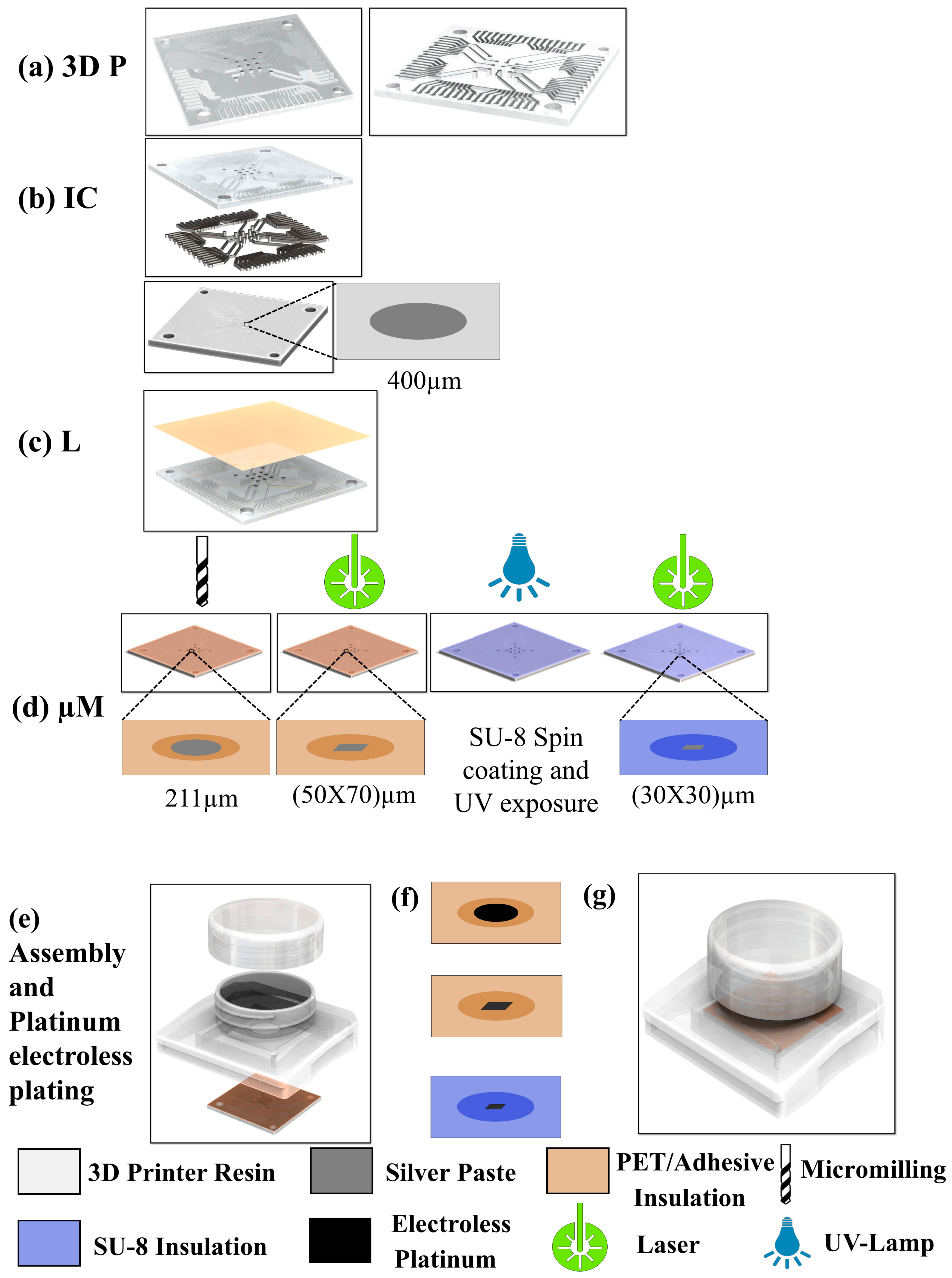
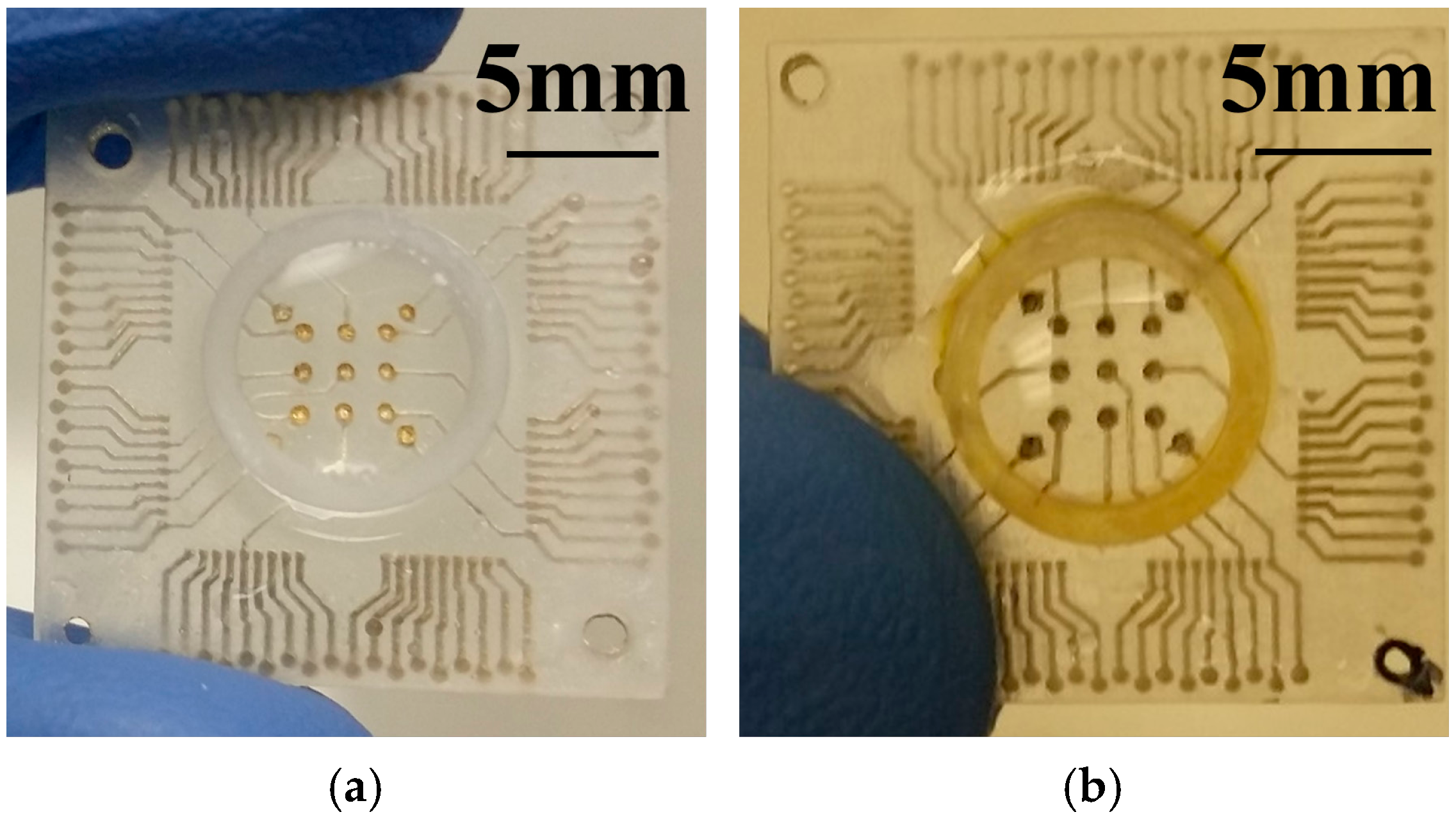
2.1. Microelectrode Arrays
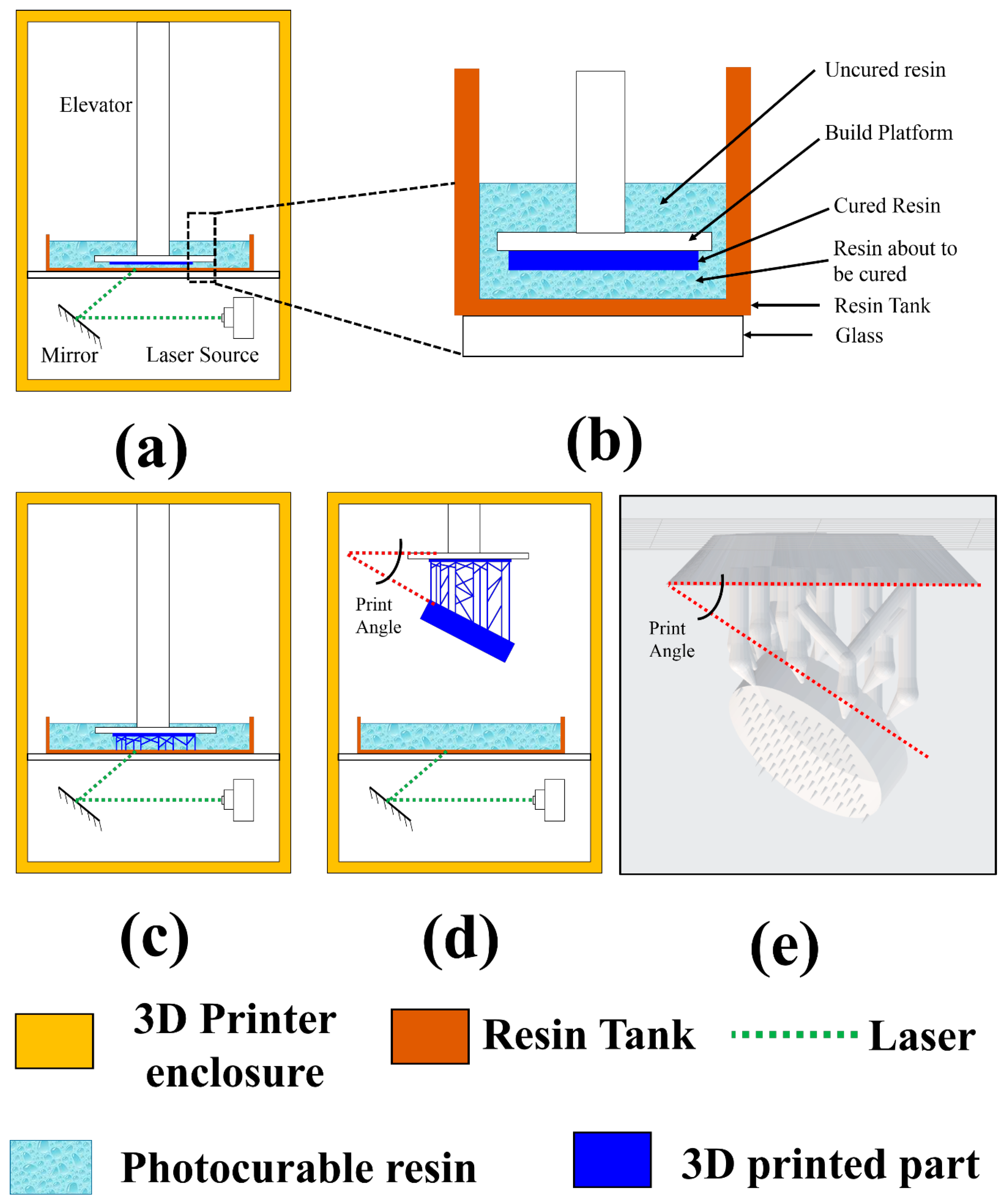
2.1.1. Design and 3D Printing
2.1.2. Ink Casting
2.1.3. Lamination
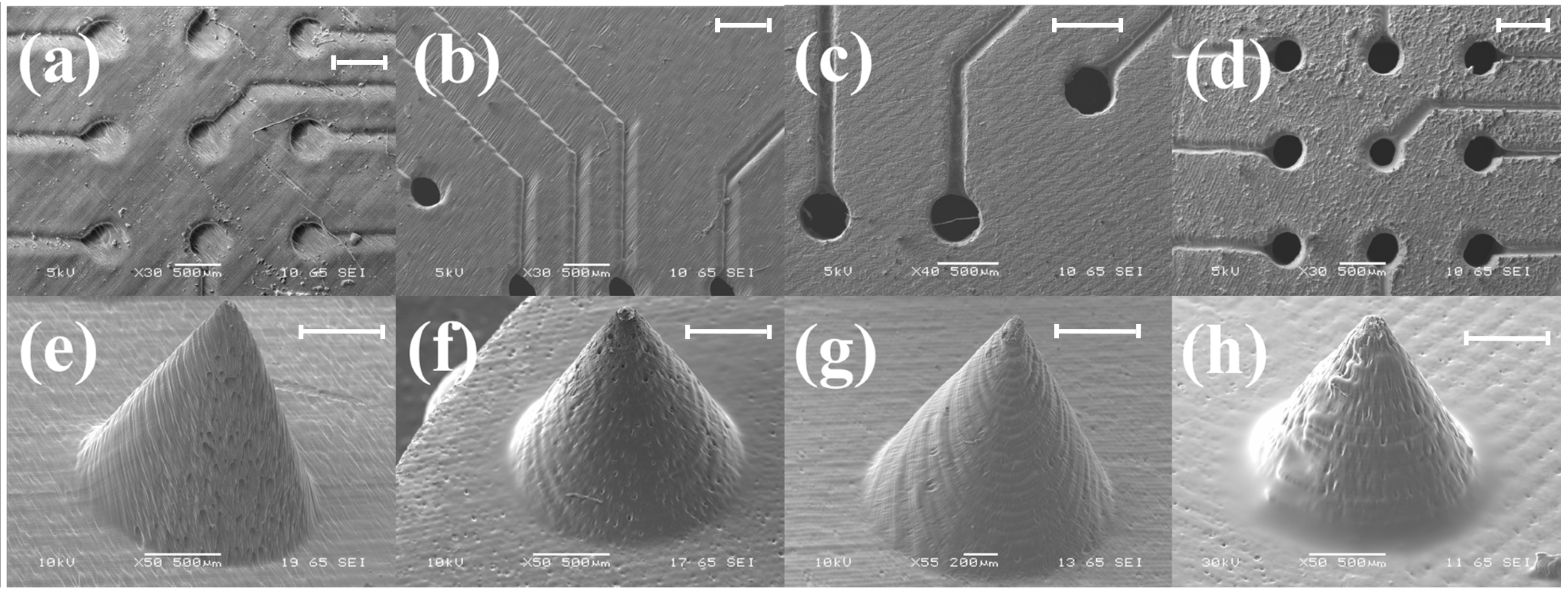
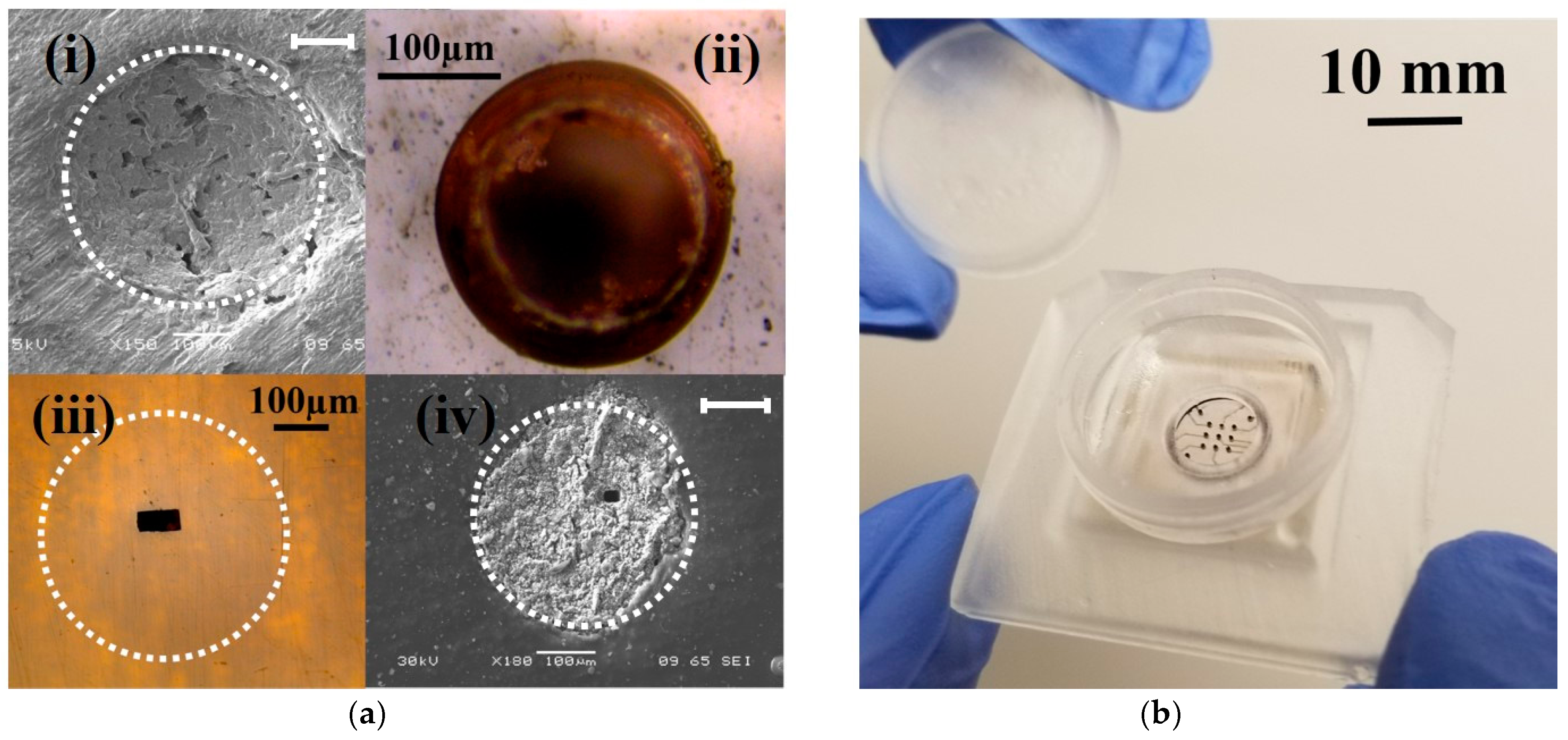
2.1.4. Subtractive Processes for Definition of MEA Recording Sites
- (a)
- Micromilling: For the fabrication of the microelectrode recording sites, an approximately 211 μm thick drill bit (T-Tech, Peachtree Corners, GA, USA) was spun at 55,000 rpm in a T-Tech J5 Quick Circuit Prototyping Systems. The total drilling time was 39 s considering a drilling speed of 180 holes/min and 13 drilling sites in a single MEA. This lamination/micromilling technique for definition of the recording sites is significantly shorter than a standard lithographic technique.
- (b)
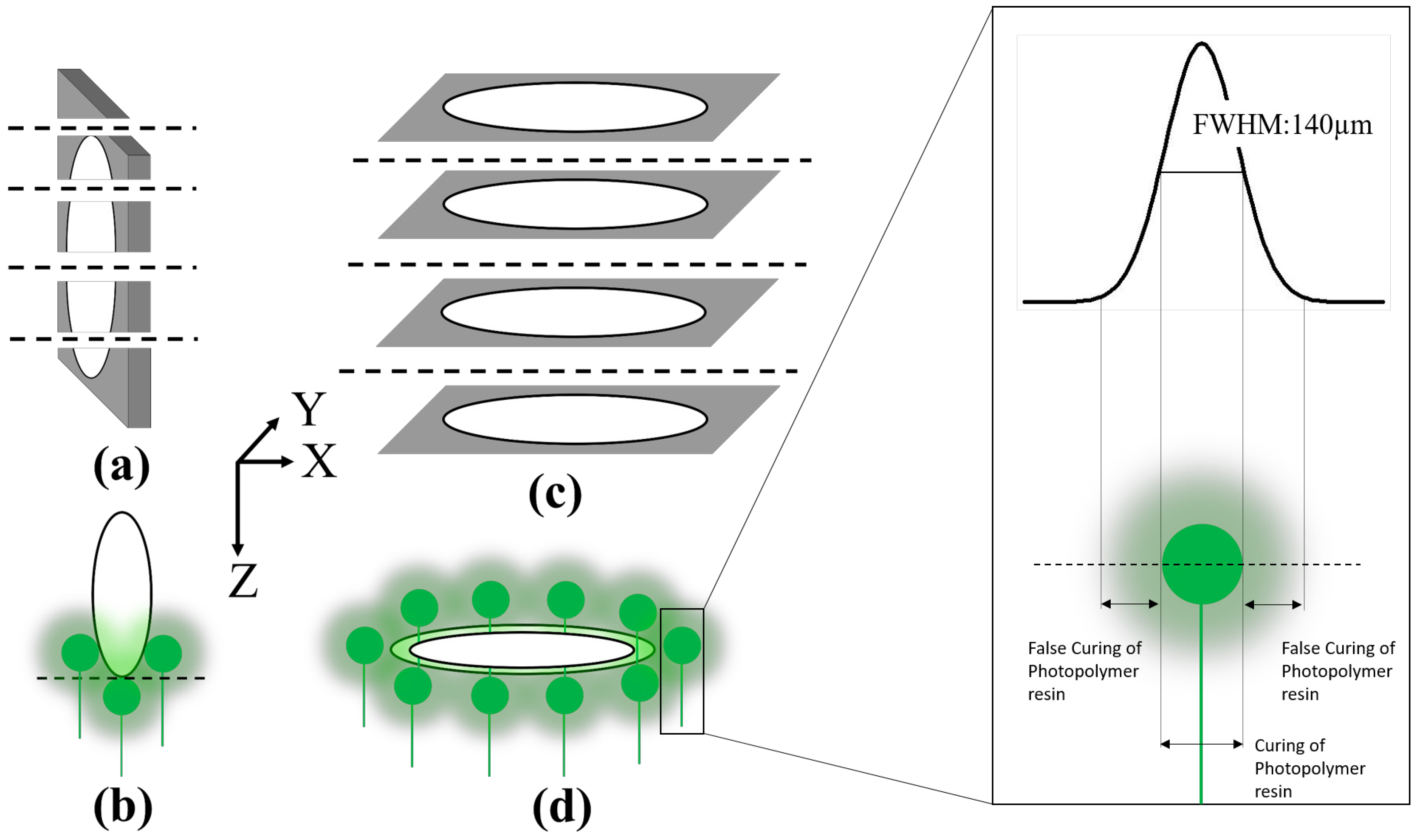
- Laser Micromachining: For the fabrication of the microelectrode recording sites, defined on the laminated adhesive using the laser, a green laser (532 nm) with a spot size of (70 μm × 50 μm) was fired at an energy level of 50 mJ at a repetition rate of 50 Hz using a QuickLaze 50ST2 (Eolite Lasers, Portland, OR, USA). The laser spot was aligned atop the lamination areas on the microelectrodes prior to the deployment of the laser. For the definition of the recording sites in the SU-8 layer, the green laser was fired with a spot size of (30 μm × 30 μm) with 25 mJ energy at a repetition rate of 50 Hz.
2.1.5. Packaging
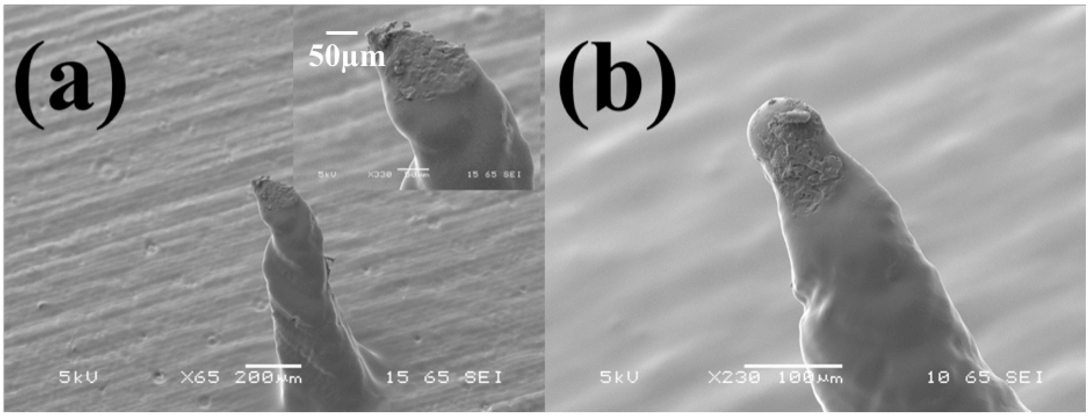
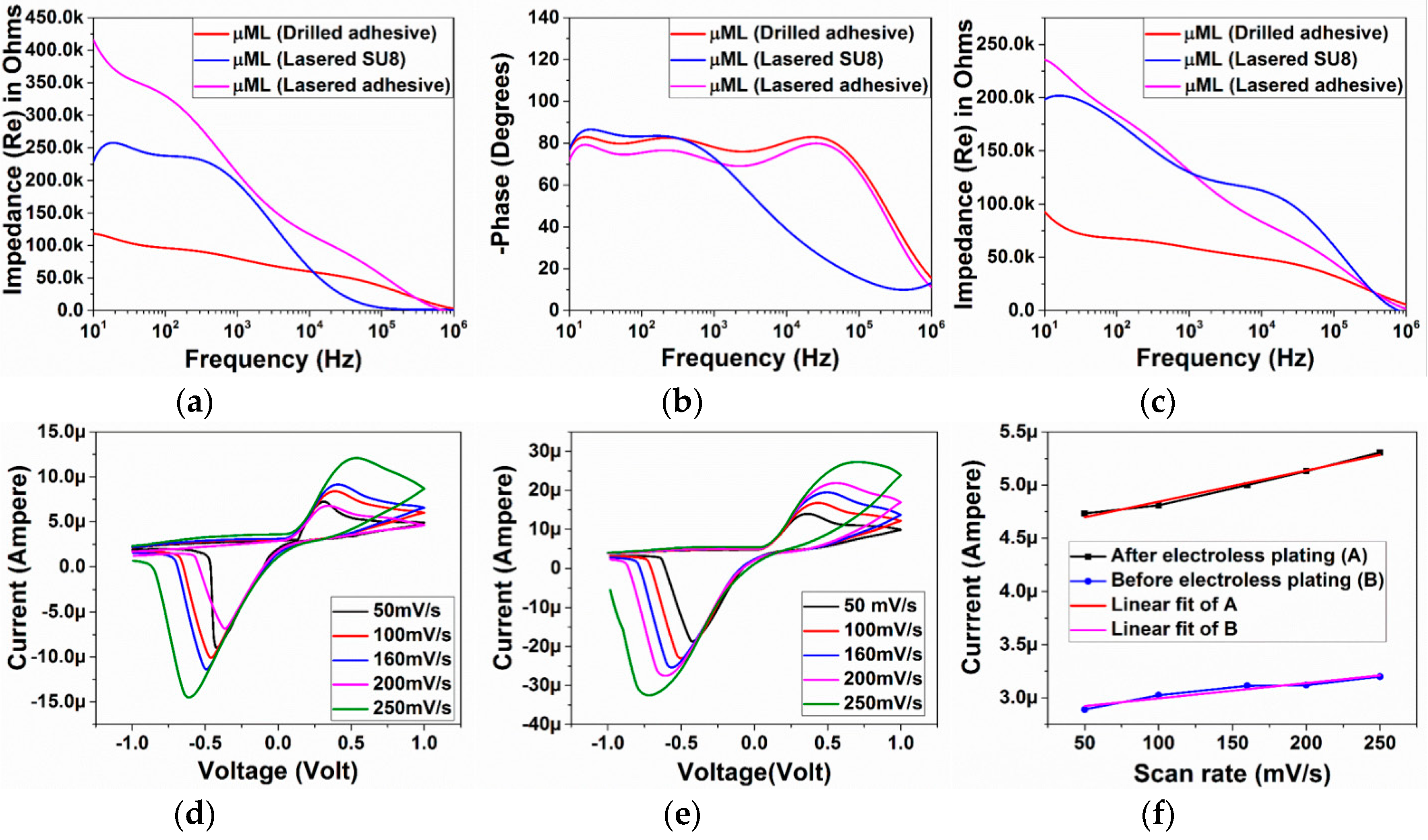
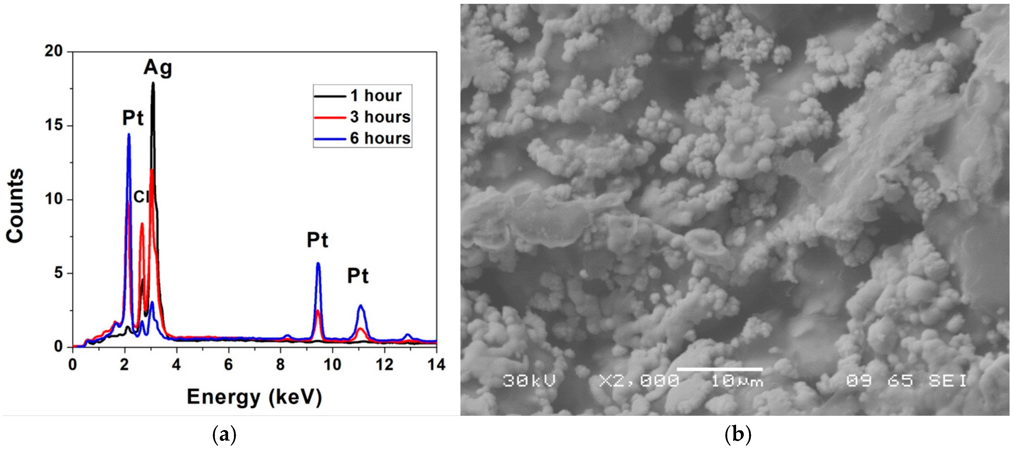
2.1.6. Electroless Plating
2.1.7. Electrical and Electrochemical Measurements
2.1.8. Imaging
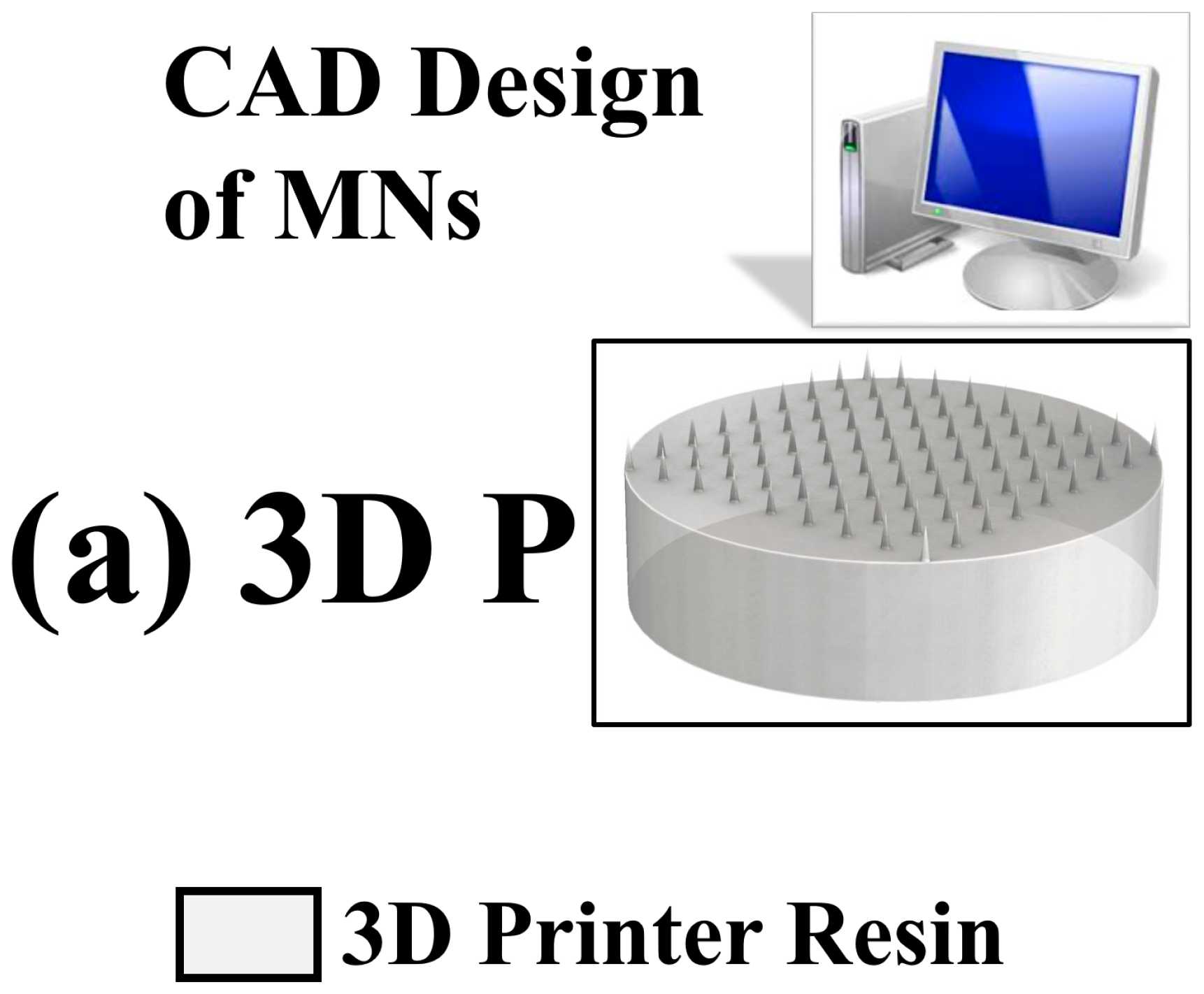
2.2. Microneedles
2.2.1. Design and 3D Printing
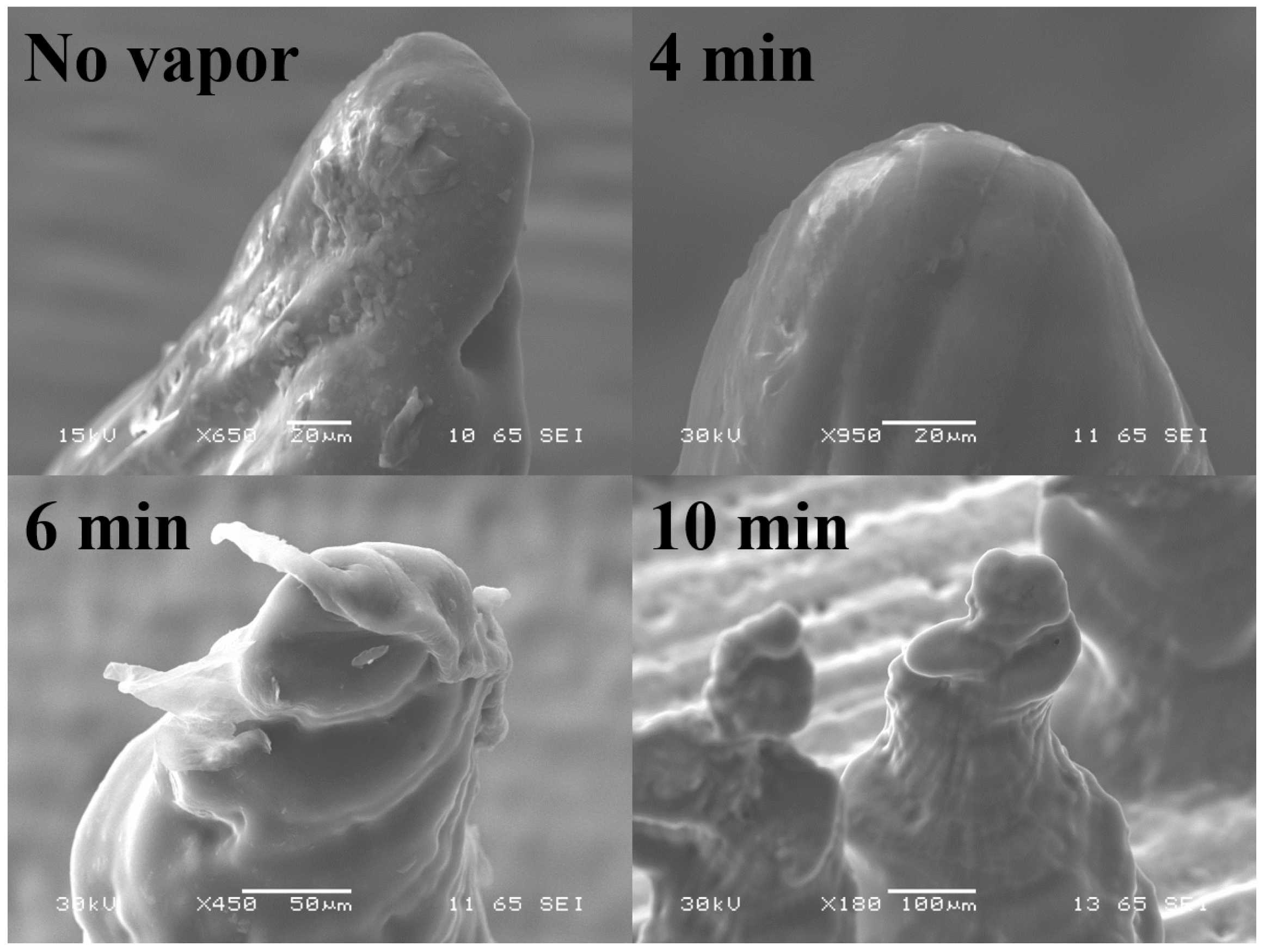
2.2.2. Acetone Vapor Polishing
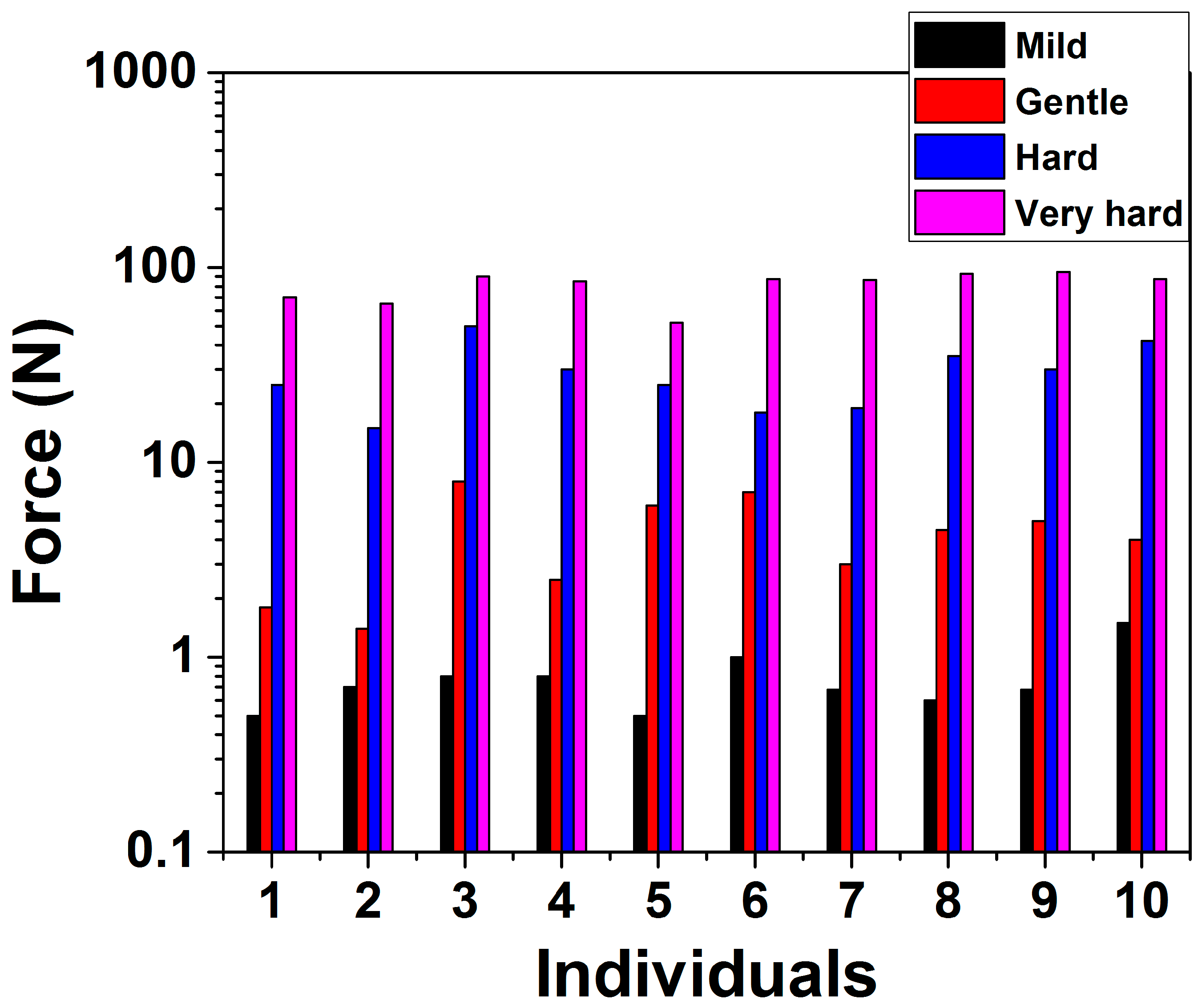
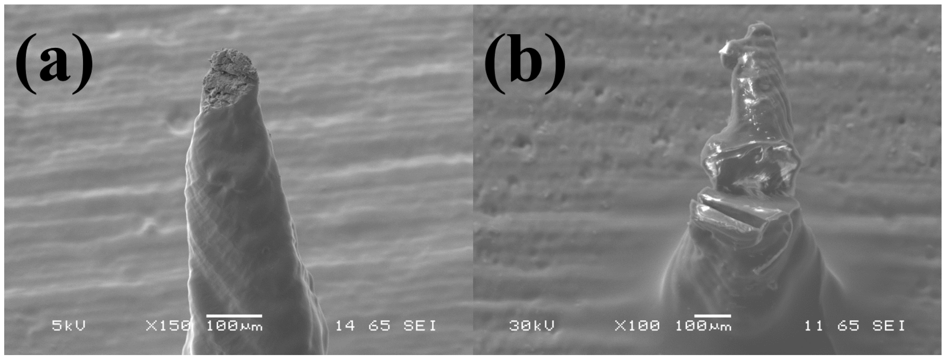
2.2.3. Measurements
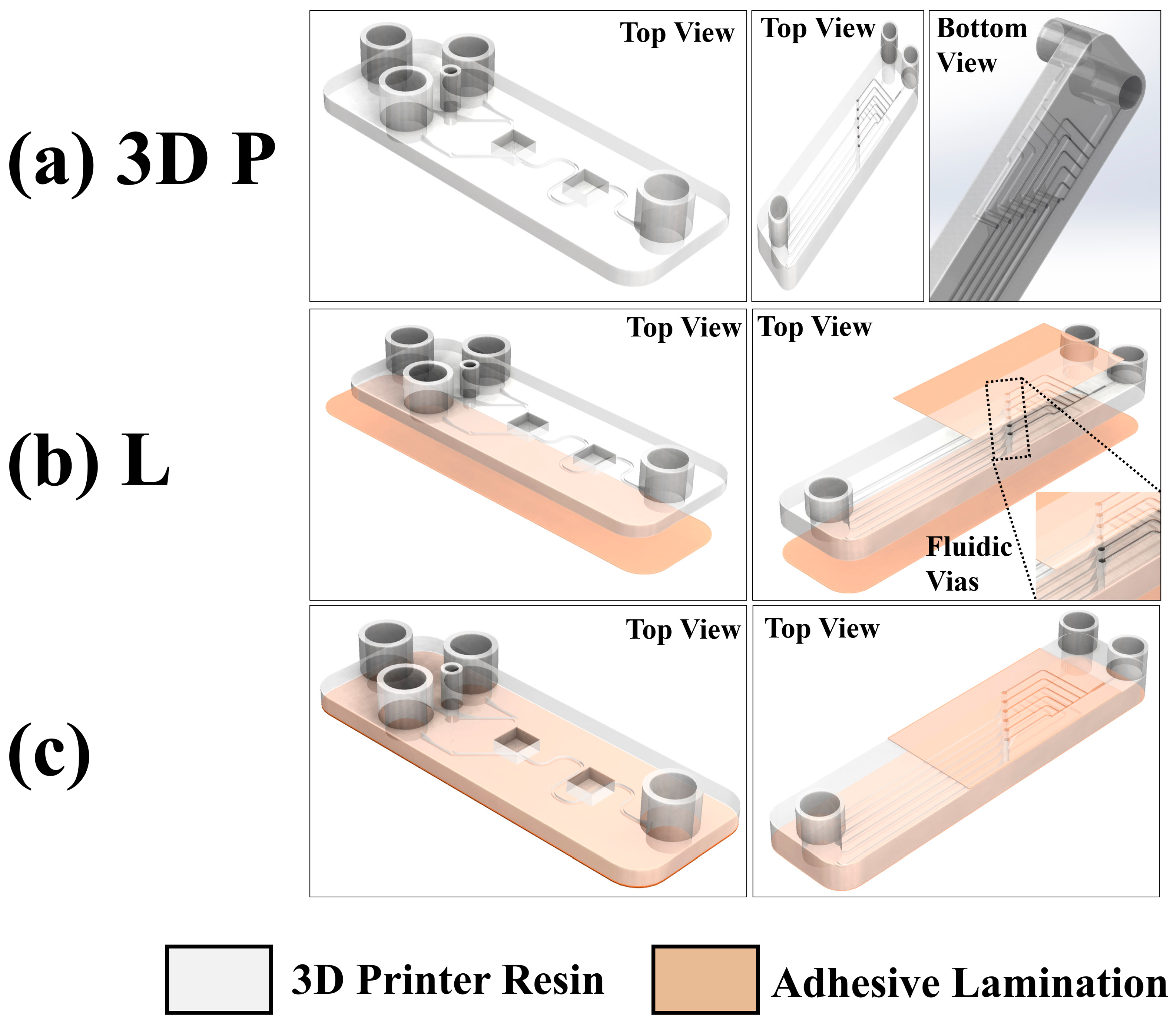
2.3. Microfluidics (MFs)
2.3.1. Design and 3D Printing
2.3.2. Lamination
2.3.3. Measurements
2.3.4. Imaging
3. Results and Discussions
3.1. 3D Print Optimization
3.1.1. Effect of Print Angle
3.1.2. Effect of Solvent Polishing
3.1.3. Effect of Temperature Curing
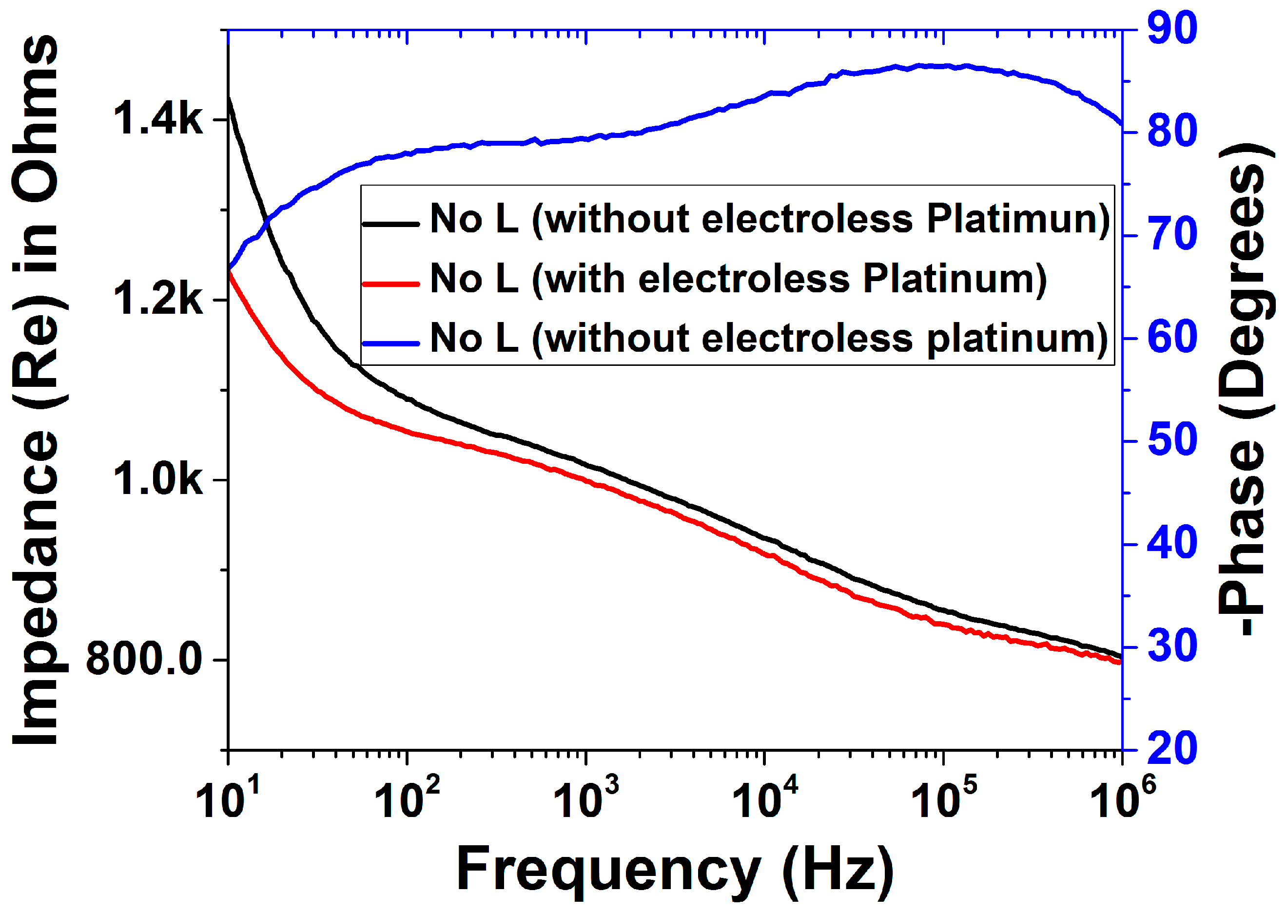
3.2. MicroElectrode Arrays
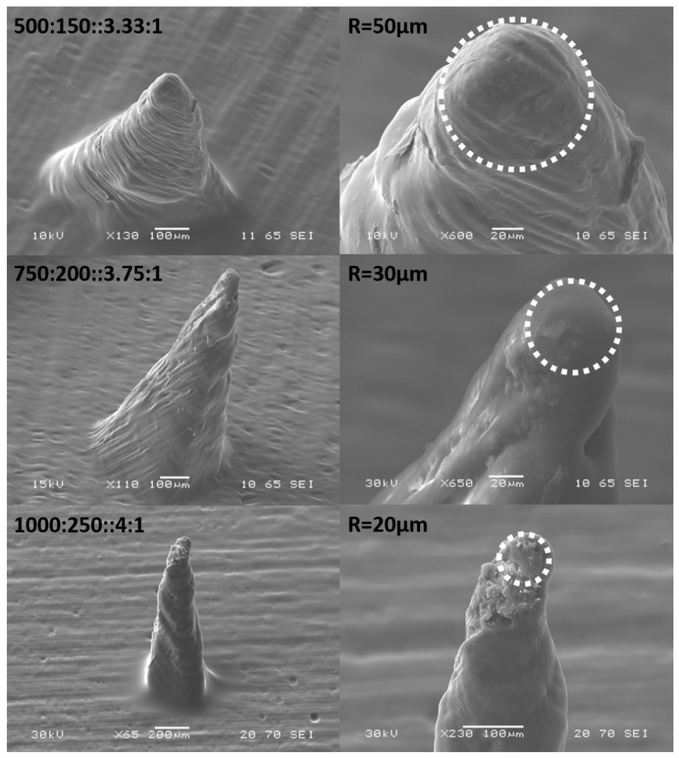
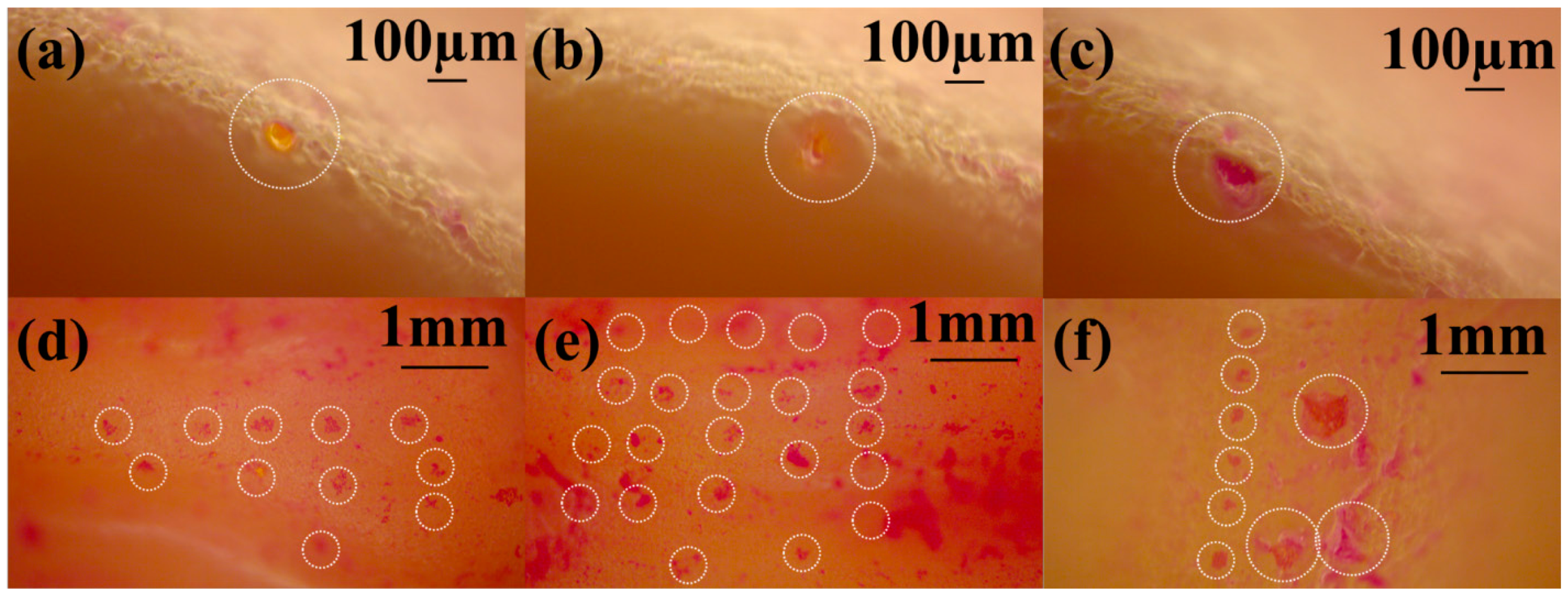
3.3. Microneedles
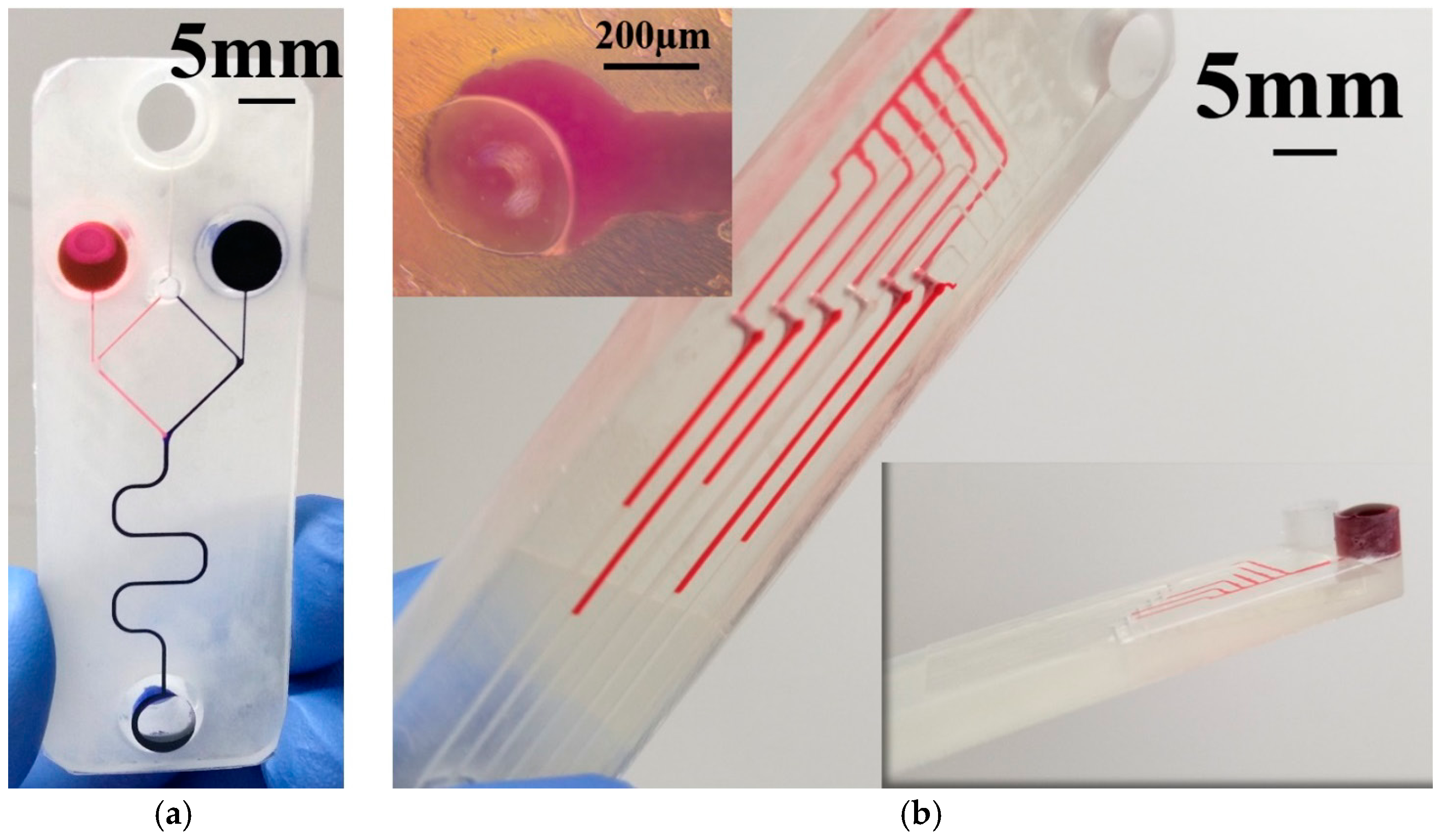
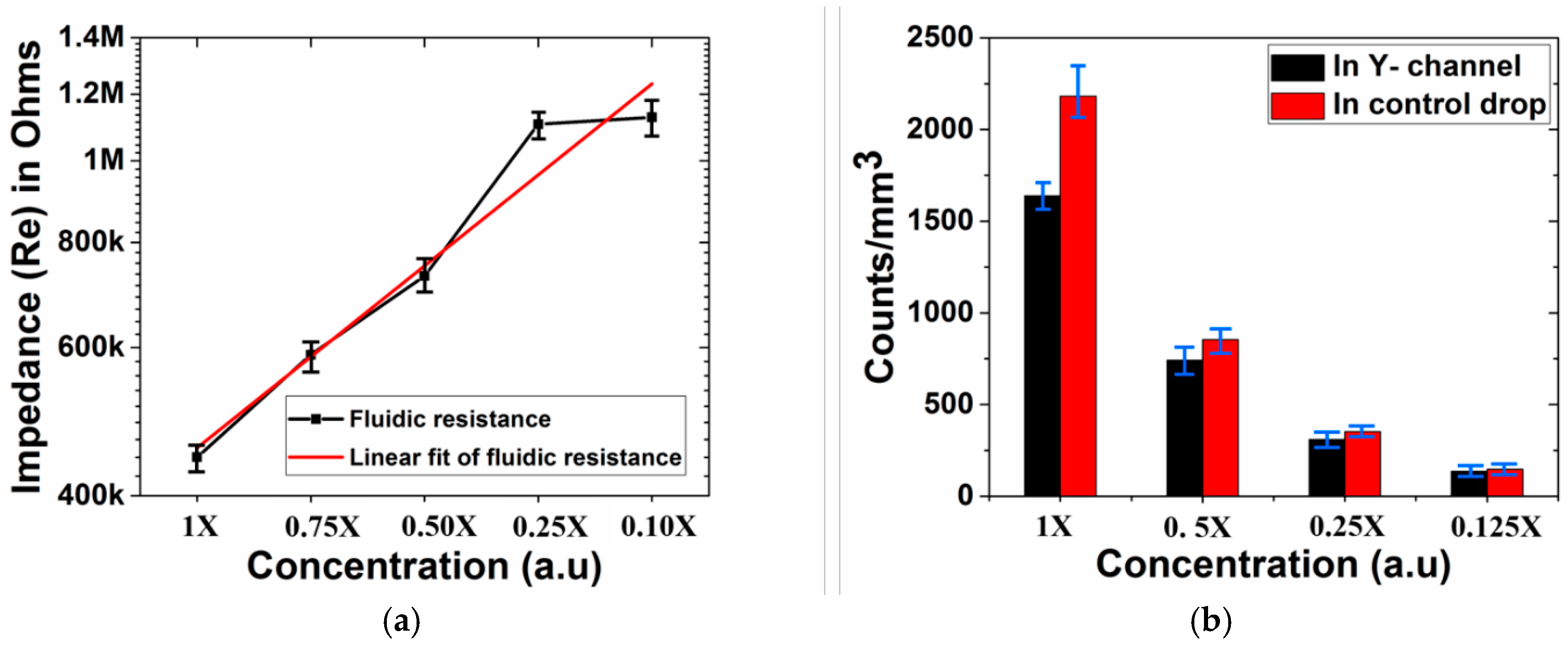
3.4. Microfluidics
4. Conclusions
Acknowledgments
Author Contributions
Conflicts of Interest
References
- Walsh, D.I.; Kong, D.S.; Murthy, S.K.; Carr, P.A. Enabling microfluidics: From clean rooms to makerspaces. Trends Biotechnol. 2017, 35, 383–392. [Google Scholar] [CrossRef] [PubMed]
- Bhattacharjee, N.; Urrios, A.; Kang, S.; Folch, A. The upcoming 3D-printing revolution in microfluidics. Lab Chip 2016, 16, 1720–1742. [Google Scholar] [CrossRef] [PubMed]
- Farooqui, M.F.; Karimi, M.A.; Salama, K.N.; Shamim, A. 3D-printed disposable wireless sensors with integrated microelectronics for large area environmental monitoring. Adv. Mater. Tech. 2017, 2. [Google Scholar] [CrossRef]
- Valentine, A.D.; Busbee, T.A.; Boley, J.W.; Raney, J.R.; Chortos, A.; Kotikian, A.; Berrigan, J.D.; Durstock, M.F.; Lewis, J.A. Hybrid 3D printing of soft electronics. Adv. Mater. 2017, 29. [Google Scholar] [CrossRef] [PubMed]
- Vizsnyiczai, G.; Frangipane, G.; Maggi, C.; Saglimbeni, F.; Bianchi, S.; Di Leonardo, R. Light controlled 3D micromotors powered by bacteria. Nat. Commun. 2017, 8, 15974. [Google Scholar] [CrossRef] [PubMed]
- Ladd, C.; So, J.H.; Muth, J.; Dickey, M.D. 3D printing of free standing liquid metal microstructures. Adv. Mater. 2013, 25, 5081–5085. [Google Scholar] [CrossRef] [PubMed]
- Gong, H.; Beauchamp, M.; Perry, S.; Woolley, A.T.; Nordin, G.P. Optical approach to resin formulation for 3D printed microfluidics. RSC Adv. 2015, 5, 106621–106632. [Google Scholar] [CrossRef] [PubMed]
- Gong, H.; Bickham, B.P.; Woolley, A.T.; Nordin, G.P. Custom 3D printer and resin for 18 μm× 20 μm microfluidic flow channels. Lab Chip 2017, 17, 2899–2909. [Google Scholar] [CrossRef] [PubMed]
- Ota, H.; Emaminejad, S.; Gao, Y.; Zhao, A.; Wu, E.; Challa, S.; Chen, K.; Fahad, H.M.; Jha, A.K.; Kiriya, D. Application of 3D printing for smart objects with embedded electronic sensors and systems. Adv. Mater. Technol. 2016, 1. [Google Scholar] [CrossRef]
- Nam, K.-H.; Smith, A.S.; Lone, S.; Kwon, S.; Kim, D.-H. Biomimetic 3D tissue models for advanced high-throughput drug screening. J. Lab Autom. 2015, 20, 201–215. [Google Scholar] [CrossRef] [PubMed]
- Konar, D.; Devarasetty, M.; Yildiz, D.V.; Atala, A.; Murphy, S.V. Lung-on-a-chip technologies for disease modeling and drug development. Biomed. Eng. Comput. Biol. 2016, 7 (Suppl. 1), 17. [Google Scholar] [CrossRef] [PubMed]
- Rezaei Kolahchi, A.; Khadem Mohtaram, N.; Pezeshgi Modarres, H.; Mohammadi, M.H.; Geraili, A.; Jafari, P.; Akbari, M.; Sanati-Nezhad, A. Microfluidic-based multi-organ platforms for drug discovery. Micromachines 2016, 7, 162. [Google Scholar] [CrossRef]
- Spira, M.E.; Hai, A. Multi-electrode array technologies for neuroscience and cardiology. Nat. Nanotechnol. 2013, 8, 83–94. [Google Scholar] [CrossRef] [PubMed]
- Kim, J.-H.; Kang, G.; Nam, Y.; Choi, Y.-K. Surface-modified microelectrode array with flake nanostructure for neural recording and stimulation. Nanotechnology 2010, 21, 085303. [Google Scholar] [CrossRef] [PubMed]
- Larraneta, E.; Lutton, R.E.; Woolfson, A.D.; Donnelly, R.F. Microneedle arrays as transdermal and intradermal drug delivery systems: materials science, manufacture and commercial development. Mater. Sci. Eng. R Rep. 2016, 104, 1–32. [Google Scholar] [CrossRef] [Green Version]
- Temiz, Y.; Lovchik, R.D.; Kaigala, G.V.; Delamarche, E. Lab-on-a-chip devices: How to close and plug the lab? Microelectron. Eng. 2015, 132, 156–175. [Google Scholar] [CrossRef]
- Wainger, B.J.; Kiskinis, E.; Mellin, C.; Wiskow, O.; Han, S.S.; Sandoe, J.; Perez, N.P.; Williams, L.A.; Lee, S.; Boulting, G. Intrinsic membrane hyperexcitability of amyotrophic lateral sclerosis patient-derived motor neurons. Cell Rep. 2014, 7, 1–11. [Google Scholar] [CrossRef] [PubMed]
- Woodard, C.M.; Campos, B.A.; Kuo, S.-H.; Nirenberg, M.J.; Nestor, M.W.; Zimmer, M.; Mosharov, E.V.; Sulzer, D.; Zhou, H.; Paull, D. iPSC-derived dopamine neurons reveal differences between monozygotic twins discordant for parkinson’s disease. Cell Rep. 2014, 9, 1173–1182. [Google Scholar] [CrossRef] [PubMed]
- Qin, Y.; Howlader, M.M.; Deen, M.J.; Haddara, Y.M.; Selvaganapathy, P.R. Polymer integration for packaging of implantable sensors. Sens. Actuator B Chem. 2014, 202, 758–778. [Google Scholar] [CrossRef]
- Kim, R.; Joo, S.; Jung, H.; Hong, N.; Nam, Y. Recent trends in microelectrode array technology for in vitro neural interface platform. Biomed. Eng. Lett. 2014, 4, 129–141. [Google Scholar] [CrossRef]
- Ita, K. Transdermal delivery of drugs with microneedles—potential and challenges. Int. J. Pharm. 2015, 7, 90–105. [Google Scholar] [CrossRef] [PubMed]
- Runyan, W.R.; Bean, K.E. Semiconductor Integrated Circuit Processing Technology; Addison Wesley Publishing Company: Boston, MA, USA, 1990. [Google Scholar]
- Chen, W.; Li, H.; Shi, D.; Liu, Z.; Yuan, W. Microneedles as a delivery system for gene therapy. Front. Pharmacol. 2016, 7, 137. [Google Scholar] [CrossRef] [PubMed]
- O’Mahony, C. Structural characterization and in vivo reliability evaluation of silicon microneedles. Biomed. Microdevices 2014, 16, 333–343. [Google Scholar] [CrossRef] [PubMed]
- Wang, P.M.; Cornwell, M.; Hill, J.; Prausnitz, M.R. Precise microinjection into skin using hollow microneedles. J. Investig. Dermatol. 2006, 126, 1080–1087. [Google Scholar] [CrossRef] [PubMed]
- Donnelly, R.F.; Singh, T.R.R.; Woolfson, A.D. Microneedle-based drug delivery systems: microfabrication, drug delivery, and safety. Drug Deliv. 2010, 17, 187–207. [Google Scholar] [CrossRef] [PubMed] [Green Version]
- Indermun, S.; Luttge, R.; Choonara, Y.E.; Kumar, P.; du Toit, L.C.; Modi, G.; Pillay, V. Current advances in the fabrication of microneedles for transdermal delivery. J. Control. Release 2014, 185, 130–138. [Google Scholar] [CrossRef] [PubMed]
- Choi, S.-O.; Kim, Y.C.; Park, J.-H.; Hutcheson, J.; Gill, H.S.; Yoon, Y.-K.; Prausnitz, M.R.; Allen, M.G. An electrically active microneedle array for electroporation. Biomed. Microdevices 2010, 12, 263–273. [Google Scholar] [CrossRef] [PubMed]
- Aoyagi, S.; Izumi, H.; Isono, Y.; Fukuda, M.; Ogawa, H. Laser fabrication of high aspect ratio thin holes on biodegradable polymer and its application to a microneedle. Sens. Actuator A Phys. 2007, 139, 293–302. [Google Scholar] [CrossRef]
- McAllister, D.V.; Wang, P.M.; Davis, S.P.; Park, J.-H.; Canatella, P.J.; Allen, M.G.; Prausnitz, M.R. Microfabricated needles for transdermal delivery of macromolecules and nanoparticles: fabrication methods and transport studies. Proc. Natl. Acad. Sci. USA 2003, 100, 13755–13760. [Google Scholar] [CrossRef] [PubMed]
- Park, J.-H.; Allen, M.G.; Prausnitz, M.R. Polymer microneedles for controlled-release drug delivery. Pharm. Res. 2006, 23, 1008–1019. [Google Scholar] [CrossRef] [PubMed]
- Han, M.; Hyun, D.-H.; Park, H.-H.; Lee, S.S.; Kim, C.-H.; Kim, C. A novel fabrication process for out-of-plane microneedle sheets of biocompatible polymer. J. Micromech. Microeng. 2007, 17, 1184. [Google Scholar] [CrossRef]
- Lippmann, J.M.; Geiger, E.J.; Pisano, A.P. Polymer investment molding: method for fabricating hollow, microscale parts. Sens. Actuator A Phys. 2007, 134, 2–10. [Google Scholar] [CrossRef]
- Sullivan, S.P.; Murthy, N.; Prausnitz, M.R. Minimally invasive protein delivery with rapidly dissolving polymer microneedles. Adv. Mater. 2008, 20, 933–938. [Google Scholar] [CrossRef] [PubMed]
- Chu, L.Y.; Choi, S.O.; Prausnitz, M.R. Fabrication of dissolving polymer microneedles for controlled drug encapsulation and delivery: bubble and pedestal microneedle designs. J. Pharm. Sci. 2010, 99, 4228–4238. [Google Scholar] [CrossRef] [PubMed]
- Kim, Y.-C.; Quan, F.-S.; Compans, R.W.; Kang, S.-M.; Prausnitz, M.R. Formulation of microneedles coated with influenza virus-like particle vaccine. Aaps Pharmscitech 2010, 11, 1193–1201. [Google Scholar] [CrossRef] [PubMed]
- Donnelly, R.F.; Majithiya, R.; Singh, T.R.R.; Morrow, D.I.; Garland, M.J.; Demir, Y.K.; Migalska, K.; Ryan, E.; Gillen, D.; Scott, C.J. Design, optimization and characterisation of polymeric microneedle arrays prepared by a novel laser-based micromoulding technique. Pharm. Res. 2011, 28, 41–57. [Google Scholar] [CrossRef] [PubMed]
- Donnelly, R.F.; McCrudden, M.T.; Alkilani, A.Z.; Larrañeta, E.; McAlister, E.; Courtenay, A.J.; Kearney, M.-C.; Singh, T.R.R.; McCarthy, H.O.; Kett, V.L. Hydrogel-forming microneedles prepared from “super swelling” polymers combined with lyophilised wafers for transdermal drug delivery. PLoS ONE 2014, 9, e111547. [Google Scholar] [CrossRef] [PubMed] [Green Version]
- Huang, H.; Fu, C. Different fabrication methods of out-of-plane polymer hollow needle arrays and their variations. J. Micromech. Microeng. 2007, 17, 393. [Google Scholar] [CrossRef]
- Ito, Y.; Hagiwara, E.; Saeki, A.; Sugioka, N.; Takada, K. Feasibility of microneedles for percutaneous absorption of insulin. Eur. J. Pharm. Sci. 2006, 29, 82–88. [Google Scholar] [CrossRef] [PubMed]
- Gittard, S.D.; Ovsianikov, A.; Chichkov, B.N.; Doraiswamy, A.; Narayan, R.J. Two-photon polymerization of microneedles for transdermal drug delivery. Expert Opin. Drug Deliv. 2010, 7, 513–533. [Google Scholar] [CrossRef] [PubMed]
- Nanoscribe GmbH. Eggenstein-Leopolds-Hafen, Germany. Available online: https://www.nanoscribe.de/en/ (accessed on 28 December 2017).
- Lu, Y.; Mantha, S.N.; Crowder, D.C.; Chinchilla, S.; Shah, K.N.; Yun, Y.H.; Wicker, R.B.; Choi, J.-W. Microstereolithography and characterization of poly (propylene fumarate)-based drug-loaded microneedle arrays. Biofabrication 2015, 7, 045001. [Google Scholar] [CrossRef] [PubMed]
- Lim, S.H.; Ng, J.Y.; Kang, L. Three-dimensional printing of a microneedle array on personalized curved surfaces for dual-pronged treatment of trigger finger. Biofabrication 2017, 9, 015010. [Google Scholar] [CrossRef] [PubMed]
- Glick, C.C.; Srimongkol, M.T.; Schwartz, A.J.; Zhuang, W.S.; Lin, J.C.; Warren, R.H.; Tekell, D.R.; Satamalee, P.A.; Lin, L. Rapid assembly of multilayer microfluidic structures via 3D-printed transfer molding and bonding. Microsyst. Nanoeng. 2016, 2, 16063. [Google Scholar] [CrossRef]
- FormLabs. Somerville, MA, USA. Available online: https://formlabs.com/blog/how-to-post-cure-3d-prints/ (accessed on 28 December 2017).
- All3DP GmbH. München, Bavaria, DE. Available online: https://all3dp.com/1/best-resin-dlp-sla-3d-printer-kit-stereolithography/ (accessed on 28 December 2017).
- Azim, N.; Sommerhage, F.; Aubin, M.; Hickman, J.; Rajaraman, S. Precision Plating of Electrogenic Cells on Microelectrodes Enhanced with Nano-Porous Platinum for Cell-Based Biosensing Applications; Meeting Abstracts; The Electrochemical Society: Pennington, NJ, USA, 2017; p. 1954. [Google Scholar]
- Karnati, C.; Aguilar, R.; Arrowood, C.; Ross, J.; Rajaraman, S. Micromachining on and of transparent polymers for patterning electrodes and growing electrically active cells for biosensor applications. Micromachines 2017, 8, 250. [Google Scholar] [CrossRef]
- Axion Biosystems. Atlanta, GA, USA. Available online: https://www.axionbiosystems.com/ (accessed on 28 December 2017).
- Multi Channel Systems MCS GmbH. Reutlingen Germany. Available online: http://www.multichannelsystems.com/ (accessed on 28 December 2017).
- Adafruit Industries LLC. New York, NY, USA. Available online: https://www.adafruit.com/product/166 (accessed on 28 December 2017).
- Juodkazis, S. Manufacturing: 3D printed micro-optics. Nat. Photonics 2016, 10, 499. [Google Scholar] [CrossRef]
- MatterHackers. Lake Forest, CA, USA. Available online: https://www.matterhackers.com/news/tech-breakdown-an-in-depth-look-at-the-moonray-s-3d-printer (accessed on 27 January 2018).
- Gallagher, A.; Ní Annaidh, A.; Bruyère, K. Proceedings of the Dynamic Tensile Properties of Human Skin, IRCOBI Conference 2012, 12–14 September 2012, Dublin (Ireland); International Research Council on the Biomechanics of Injury: Dublin, Ireland, 2012. [Google Scholar]
- Ripolin, A.; Quinn, J.; Larrañeta, E.; Vicente-Perez, E.M.; Barry, J.; Donnelly, R.F. Successful application of large microneedle patches by human volunteers. Int. J. Pharm. 2017, 521, 92–101. [Google Scholar] [CrossRef] [PubMed]
- Shipulya, N.; Konakov, S.; Krzhizhanovskaya, V. Development and simulation of microfluidic wheatstone bridge for high-precision sensor. J. Phys. Conf. Ser. 2016, 738, 012071. [Google Scholar] [CrossRef]


© 2018 by the authors. Licensee MDPI, Basel, Switzerland. This article is an open access article distributed under the terms and conditions of the Creative Commons Attribution (CC BY) license (http://creativecommons.org/licenses/by/4.0/).
Share and Cite
Kundu, A.; Ausaf, T.; Rajaraman, S. 3D Printing, Ink Casting and Micromachined Lamination (3D PICLμM): A Makerspace Approach to the Fabrication of Biological Microdevices. Micromachines 2018, 9, 85. https://doi.org/10.3390/mi9020085
Kundu A, Ausaf T, Rajaraman S. 3D Printing, Ink Casting and Micromachined Lamination (3D PICLμM): A Makerspace Approach to the Fabrication of Biological Microdevices. Micromachines. 2018; 9(2):85. https://doi.org/10.3390/mi9020085
Chicago/Turabian StyleKundu, Avra, Tariq Ausaf, and Swaminathan Rajaraman. 2018. "3D Printing, Ink Casting and Micromachined Lamination (3D PICLμM): A Makerspace Approach to the Fabrication of Biological Microdevices" Micromachines 9, no. 2: 85. https://doi.org/10.3390/mi9020085
APA StyleKundu, A., Ausaf, T., & Rajaraman, S. (2018). 3D Printing, Ink Casting and Micromachined Lamination (3D PICLμM): A Makerspace Approach to the Fabrication of Biological Microdevices. Micromachines, 9(2), 85. https://doi.org/10.3390/mi9020085