A Low Power Energy-Efficient Precision CMOS Temperature Sensor †


College of Physics and Information Engineering, Fuzhou University, Fuzhou 350116, Fujian, China
*
Author to whom correspondence should be addressed.
†
This work was supported by the National Natural Science Foundation of China (Grant No. 61404030) and the Natural Science Foundation of Fujian Province, China (Grant No. 2018J01803).
Micromachines 2018, 9(6), 257; https://doi.org/10.3390/mi9060257
Submission received: 11 April 2018
/
Revised: 11 May 2018
/
Accepted: 17 May 2018
/
Published: 24 May 2018
(This article belongs to the Special Issue Interface Circuits for Microsensor Integrated Systems)
Abstract
:This paper presents a low power, energy-efficient precision CMOS temperature sensor. The front-end circuit is based on bipolar junction transistors, and employs a pre-bias circuit and bipolar core. To reduce measurement errors arising from current ratio mismatch, a new dynamic element-matching mode is proposed, which dynamically matches all current sources in the front-end circuit. The first-order fitting and third-order fitting are used to calibrate the output results. On the basis of simulation results, the sensor achieves 3σ-inaccuracies of +0.18/−0.13 °C from −55 °C to +125 °C. Measurement results demonstrate sensor 3σ-inaccuracies of ±0.2 °C from 0 °C to +100 °C. The circuit is implemented in 0.18 μm CMOS, and consumes 6.1 μA with a 1.8 V supply voltage.
1. Introduction
Knowing the die temperature of transistors employed in precision sensor systems is often quite important because this information can be used to mitigate the cross sensitivity of a system to temperature [1,2]. In this manner, temperature sensors have been employed to compensate for the temperature dependence of MEMS resonators [1], to compensate for the curvature in a band-gap voltage reference [2], or in temperature measurements and over-temperature protection directly. In such systems, the inaccuracy of temperature sensors is a significant component of the total error budget, and thus often limits their ultimate performance.
Wu et al. [3] presented a thermistor-based sensor that achieved an inaccuracy of ±0.5 °C from 0 °C to 100 °C with one-point calibration. Although a thermistor-based sensor has the advantage of low power consumption, it usually requires multi-point calibration to attain high accuracy because of the non-linearity between resistance and temperature. Chen et al. [4] proposed a time-to-digital converter based temperature sensor that achieved an inaccuracy of −0.7/+0.9 °C from 0 °C to 100 °C. Testi et al. [5] presented a ring oscillator-based temperature sensor that achieved a maximum inaccuracy of ±3 °C from 0 °C to 120 °C after two-point calibration. While both of these latter temperature sensors have the advantage of low power consumption, they failed to achieve high accuracies.
Sensors based on bipolar junction transistors (BJTs) can achieve high accuracy because the base-emitter voltage VBE offers advantageous temperature characteristics. Lee et al. [6] proposed a BJT-based temperature sensor that achieved an inaccuracy of ±1 °C from −55 °C to 125 °C. Aita et al. [7] presented a BJT-based temperature sensor that achieved an inaccuracy of ±0.25 °C from −70 °C to 130 °C using dynamic element matching (DEM).
This paper proposes a temperature sensor circuit based on BJTs for operation over the temperature range of 0 °C to 100 °C. Compared with the DEM approaches employed previously to reduce mismatch related errors [8,9], we propose a new DEM approach, denoted as all DEM (ALL-DEM), that provides greater temperature measurement precision by dynamically matching all current sources in the front-end circuit. Moreover, compared with the employment of a second-order sigma-delta analog-to-digital converter (ADC) [10] and a first-order zoom ADC [11], the sensor employs a second-order zoom ADC, which can improve the resolution and reduce the required conversion time. In addition, the temperature sensor employs voltage calibration to improve its performance.
The remainder of this paper is organized as follows. Section 2 describes the operation of the BJT-based temperature sensor front-end circuit, and discusses its main error sources. Section 3 discusses the proposed temperature sensor front-end circuit employing the ALL-DEM approach in detail. Section 4 describes the structure and operating modes of a zoom ADC. Section 5 discusses the voltage calibration and the means of conducting first-order fitting and third-order fitting. Section 6 presents the simulation and measurement results of the chip and discusses this work. Section 7 concludes the paper.
2. Sensor Operating Principles and Error Budgeting
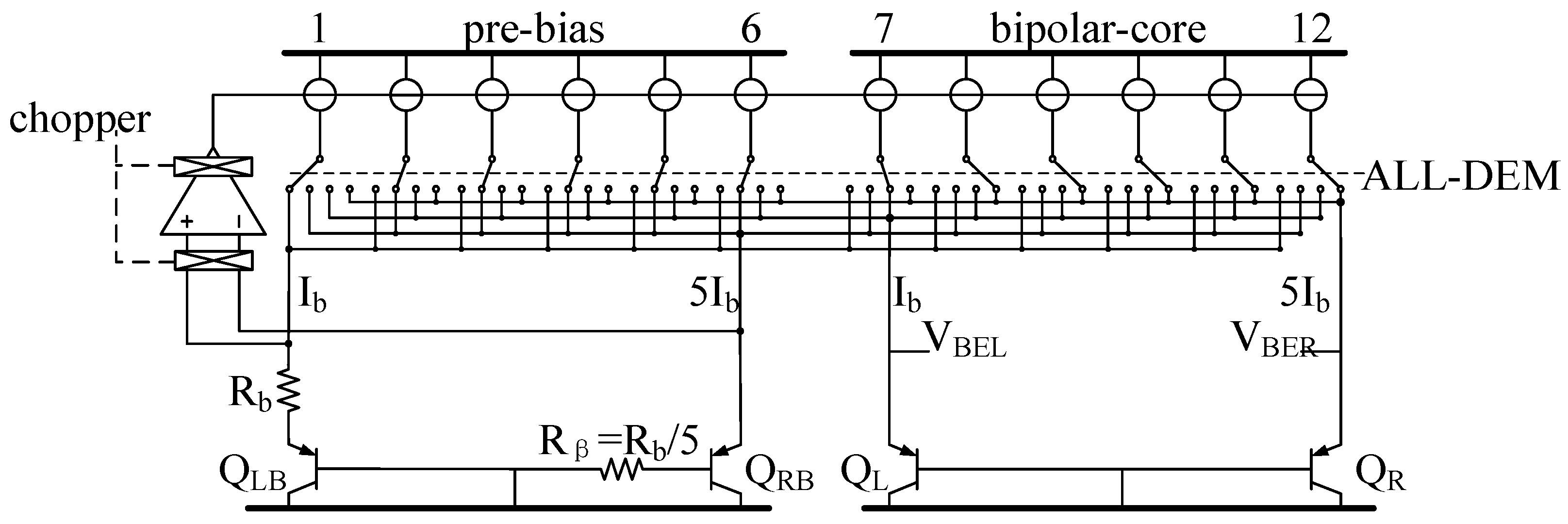
As shown in Figure 1, the front-end circuit consists of a pre-bias circuit and a bipolar core built around several current sources, four substrate PNP transistors, and an opamp. Two branches of current with a ratio of 1:pb bias a pair of PNPs (QLB and QRB).
The base-emitter voltages VBE of the PNPs (VBELB and VBERB) are complementary to the absolute temperature (CTAT), whereas the difference between the two values of VBE, denoted as ∆VBE_PB, is proportional to the absolute temperature (PTAT). For a BJT, these voltages can be given by
respectively, where η is a process-dependent nonideality factor, k is the Boltzmann constant, q is the electron charge, T is the temperature in Kelvin, and IC and IS are the collector and saturation currents of the BJT. An opamp forces ∆VBE_PB across a resistance of Rb to generate a PTAT bias current Ib = ∆VBE_PB/Rb. The PTAT current is mirrored to the bipolar core, and two current branches with a ratio of 1:p are directed to two PNPs (QL and QR) to generate two additional VBE (VBEL and VBER) and ∆VBE_BC values.
Because the current gain β of the PNPs is finite and the biasing current is directed to a PNP via its emitter, the ratio of IC (QLB and QRB) is not the same as a current branch. Using a β-compensating resistance of Rβ = Rb/5 in the pre-bias circuit suppresses the effect of β on VBE [12].
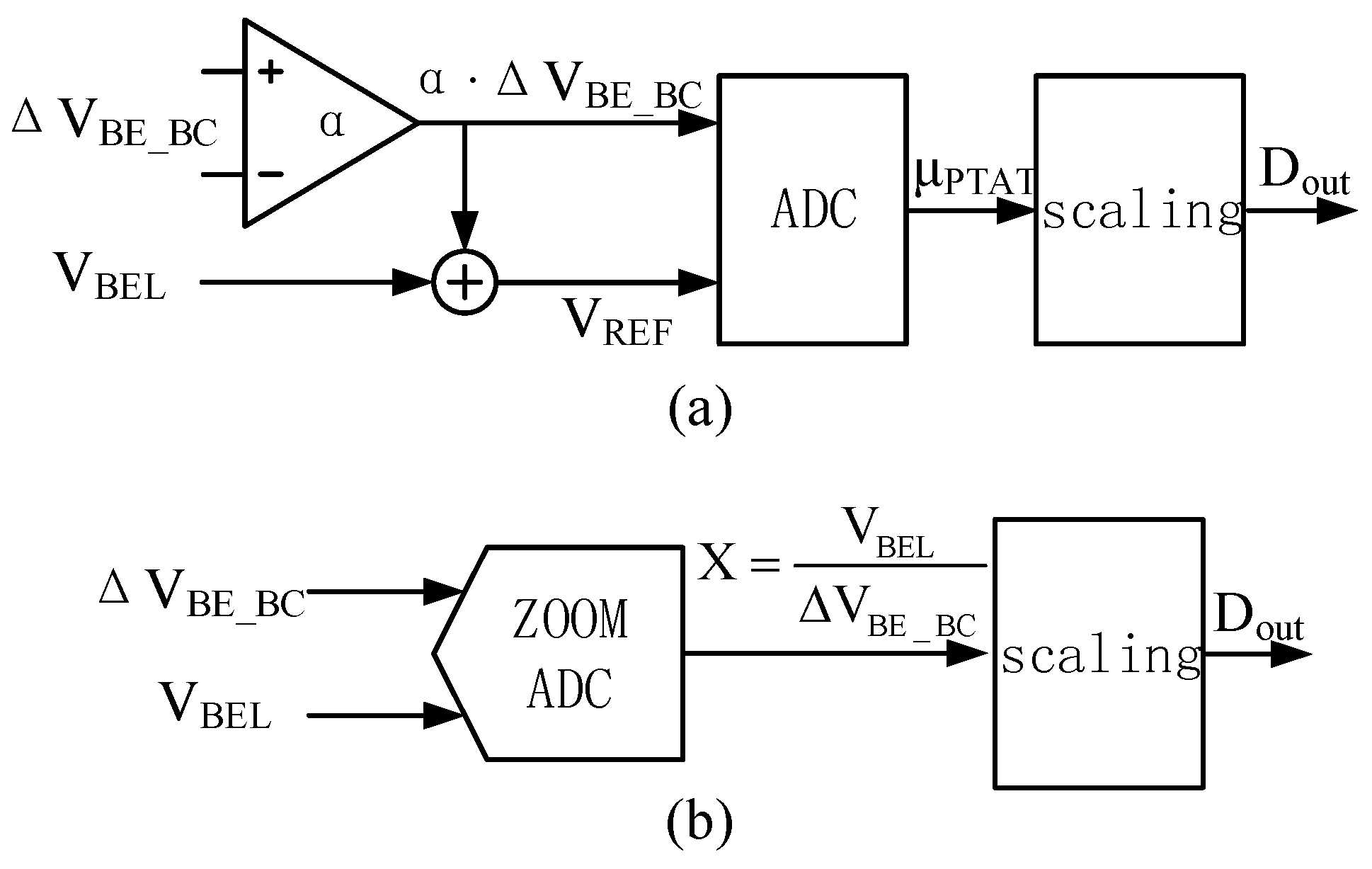
Generally, as shown in Figure 2a, temperature can be measured as α·∆VBE with respect to a reference voltage VREF = VBEL + α·∆VBE_BC, where α is a constant [9]. This provides the parameter μPTAT = α·∆VBE_BC/VREF, which varies linearly from ~0.3 to ~0.7 over the temperature range considered [12]. Alternatively, as shown in Figure 2b, a zoom ADC is employed for this purpose to reduce the power consumption, die area, and required conversion time [8,13].
The ADC provides the parameter X = VBEL/∆VBE_BC, which varies nonlinearly from ~28 to ~8 over the temperature range considered [8]. In this case, the parameter μPTAT can be determined in the digital back-end according to the relationship μPTAT = X/(α + X), where α is a calibration parameter. The discretized output Dout based on the parameter μPTAT can then be converted to units of °C by a linear fit as follows [8]:
Here, A and B are calibration parameters with approximate values of 600 and −273, respectively.
According to Equation (3), the sensitivity of Dout to error in VBEL and ∆VBE_BC can be respectively expressed by
where the approximation μPTAT ≈ T/A has been employed in the final forms. For example, supposing that VREF = 1.2 V, A = 600, and α = 14, a 0.1 °C temperature error is approximately equal to a 0.3 mV error in VBEL at +126.85 °C or a 0.02 mV error in ∆VBE_BC at −73.15 °C. Therefore, the accuracy of the sensor is limited by the error in VBEL and ∆VBE_BC.
The main source of error in ∆VBE_BC is a current ratio mismatch ∆p between the two current branches in the bipolar core. The absolute error in ∆VBE_BC can then be given as follows:
Here, T is in units of Kelvin. With a carefully designed layout of the current sources, ∆p/p = 0.1% can be expected [14], and the temperature error due to mismatch is then 0.091 K according to Equation (5).
Error due to ∆p can be reduced by dynamically interchanging the current sources in the bipolar core [15] using DEM [16]. This is illustrated for the case of the bipolar core in Figure 1. One of the current sources is directed to QL, whereas the other current sources are directed to QR. This averaging process cancels the first-order error in ∆VBE_BC whereas the second-order error remains, which is given as follows [12]:
If, for instance, ∆p/p = 1%, this corresponds to a temperature error of at most 4.6 mK, which is sufficient to obtain a temperature error well below 0.1 K.
Similarly, a current ratio mismatch exists in the pre-bias circuit, which results in PTAT errors in Ib and VBEL. The absolute error in VBEL can then be given as follows:
If, for example, ∆p/p = 1%, the error in VBEL corresponds to a temperature error of at most 65 mK.
3. Temperature Sensor Front-End Circuit
According to the discussion in the previous section, a conventional circuit reduces temperature measurement errors by averaging ∆p to some extent, but cannot make full use of the circuit because current sources in the pre-bias circuit do not participate in the averaging process. Therefore, we employed the proposed ALL-DEM approach in the temperature sensor front-end circuit, which matches all current sources in both the pre-bias circuit and bipolar core dynamically. Assuming that pb = p = 5, the proposed circuit is illustrated in Figure 3.
The ALL-DEM approach employs the following steps:
Step 1: Number all current sources from 1 to 12.
Step 2: Under the control of ALL-DEM, current source 1 is directed to QLB, current sources 2–6 are directed to QRB, current source 7 is directed to QL, and current sources 8–12 are directed to QR.
Step 3: After a single integral sampling period, current sources are cyclically shifted, and Step 2 is repeated, i.e., current source 2 is directed to QLB, current sources 3–7 are directed to QRB, current source 8 is directed to QL, and current sources 9–12 and current source 1 are directed to QR.
An ALL-DEM cycle consists of 12 periods. In addition to dynamically matching the current sources in the pre-bias circuit (rather than only in the bipolar core), the ALL-DEM approach offers another advantage, in that it provides a greater number of conditions in the bipolar core compared with conventional DEM, which is increased from 6 to 12.
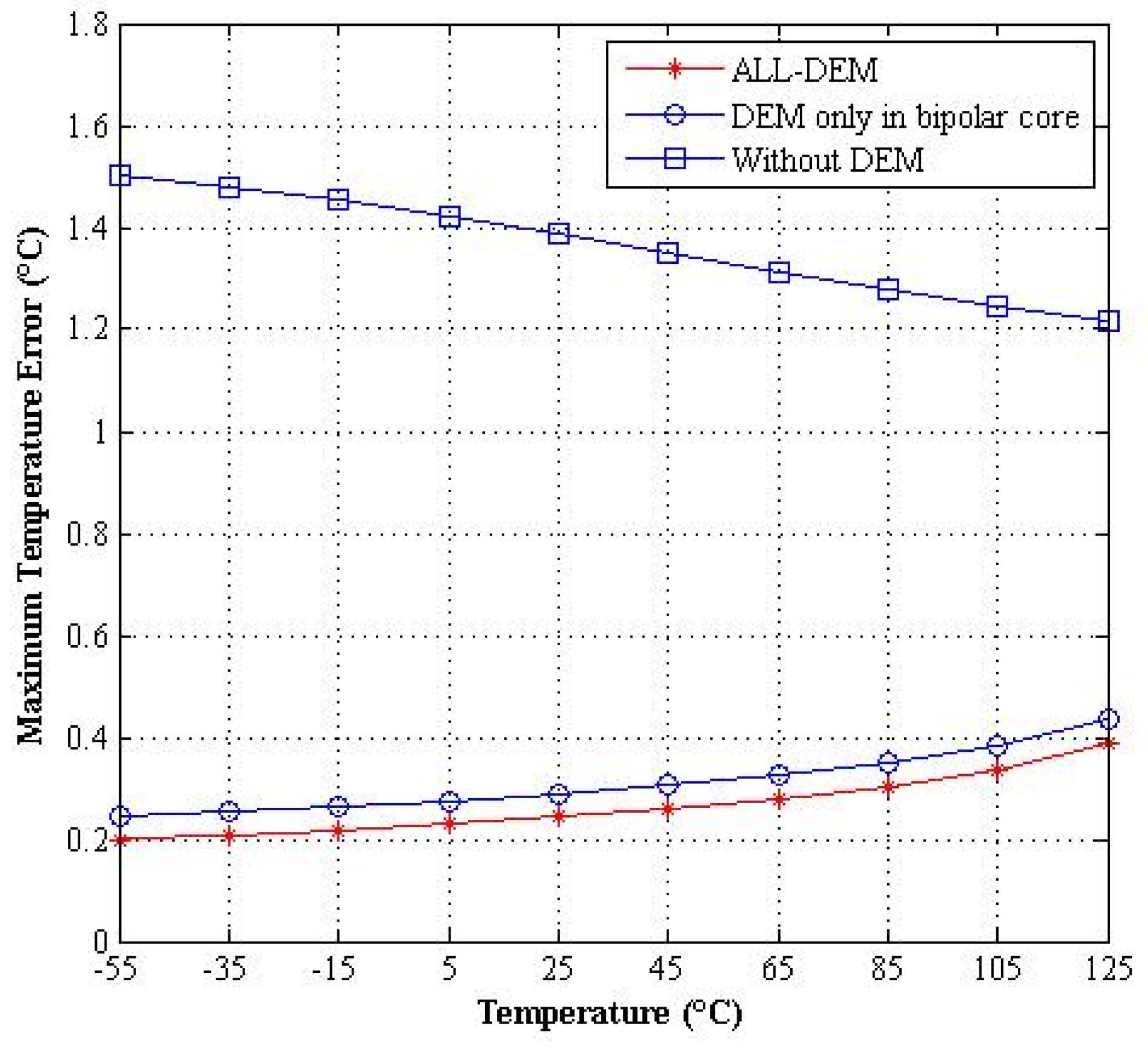
The ALL-DEM approach can reduce the mismatch in the pre-bias circuit, and, hence, can reduce temperature measurement errors caused by the pre-bias circuit. In addition, the proposed circuit employs chopping to suppress the offset of the opamp. The benefits of the ALL-DEM approach are demonstrated by the simulation results presented in Figure 4, which shows the maximum temperature errors obtained with different DEM schemes. As the results show, the maximum temperature error caused by the ALL-DEM approach is at least 0.82 °C less than that obtained without the DEM approach. Moreover, the average maximum temperature error caused by the ALL-DEM approach is 0.07 °C less than that of the conventional DEM approach. The ALL-DEM approach can therefore achieve a higher accuracy than the conventional DEM approach.
4. Zoom Analog-to-Digital Converter
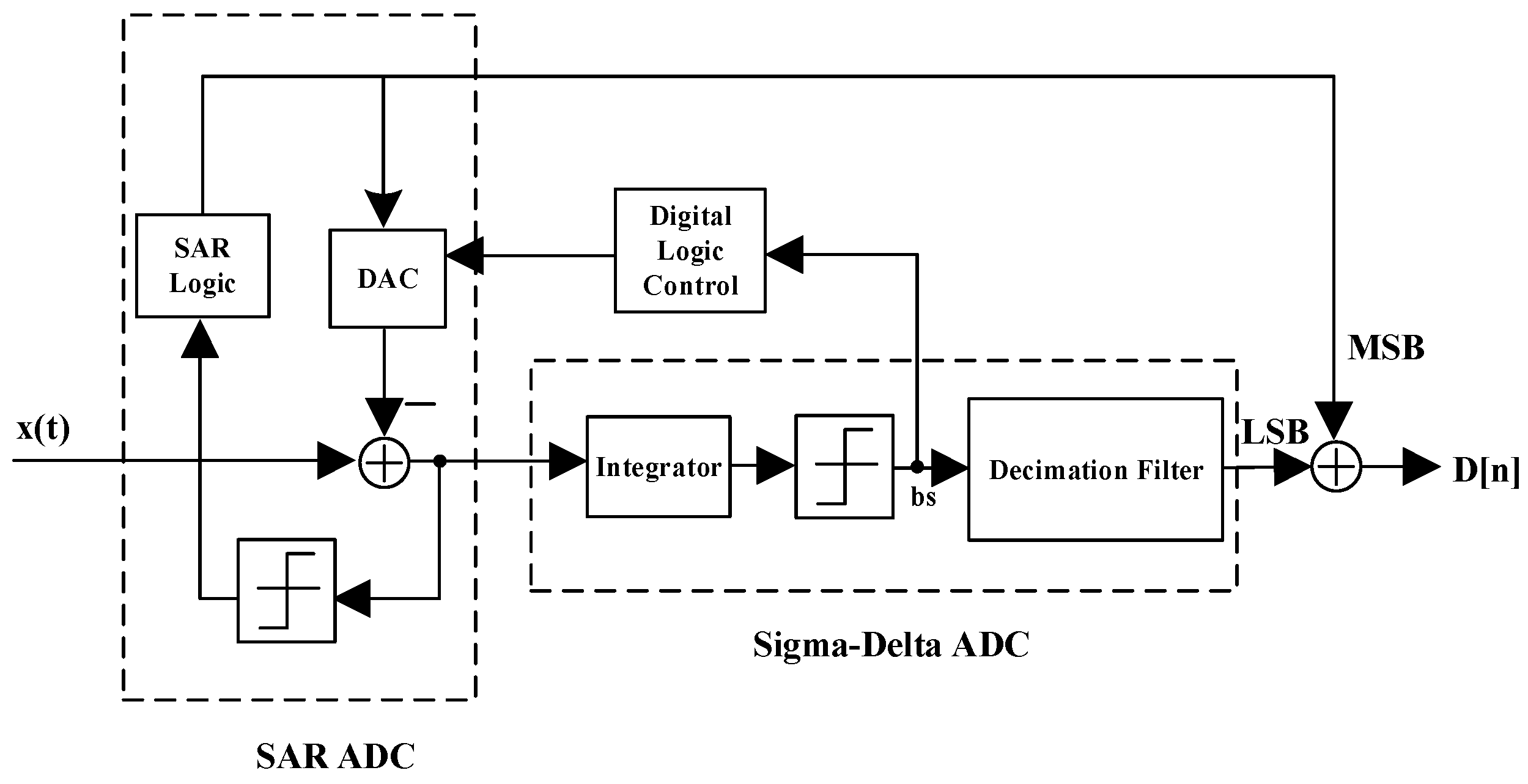
As shown in Figure 5, the zoom ADC is a two-step ADC structure that consists of a successive approximation (SAR) ADC and a sigma-delta ADC. The conversion process of the zoom ADC can be divided into two operating modes. Here, the SAR ADC first converts the input x(t) to obtain the output of the most significant bit (MSB), which is denoted as coarse conversion. Then, the zoom ADC enters into the second operating mode, where the sigma-delta ADC converts the input x(t) according to MSB, and generates the output of the least significant bit (LSB), which is denoted as fine conversion. Finally, we obtain the output D[n] by combining MSB and LSB. Therefore, the zoom ADC combines the rapid conversion of an SAR ADC with the high precision of a sigma-delta ADC.
5. Calibration
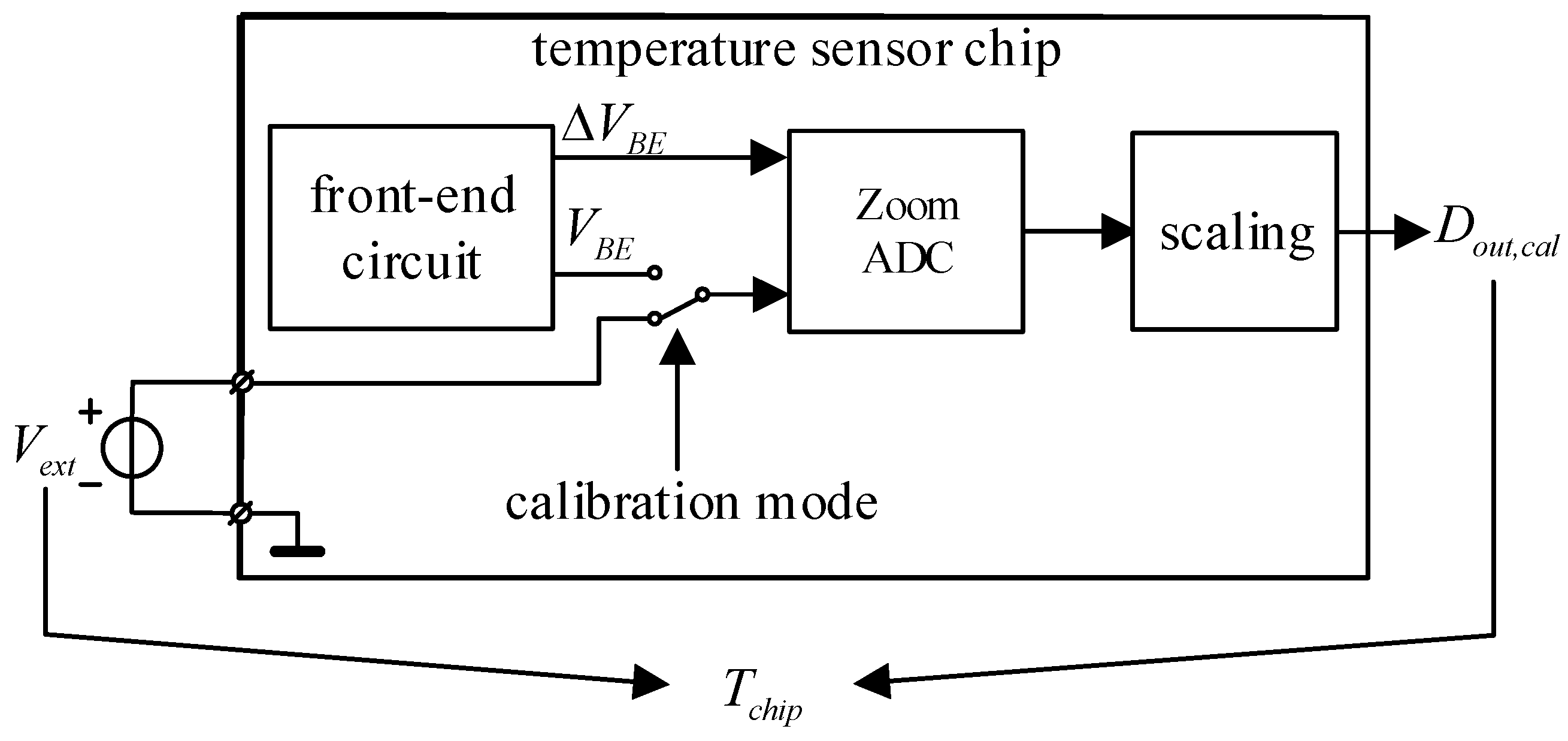
Figure 6 presents an overview of the temperature sensor. It consists of a front-end circuit that generates VBE and ∆VBE, which are fed to the zoom ADC. The output of the zoom ADC in the normal operating mode is the ratio XN = VBE/∆VBE. However, the ADC can be configured to output Xc = Vext /∆VBE when the temperature sensor chip is placed in the calibration mode. A PT-100 thermistor, which was calibrated to an error of less than 1 mK and placed in good thermal contact with the temperature sensor, was used to obtain the reference temperature Tchip [17].
We adopted voltage calibration, which employs the following steps.
Step 1: Change the operating mode of the temperature sensor chip into the calibration mode. Then, input testing voltage Vext, and obtain ∆VBE as follows:
We can then calculate η using ∆VBE and Tchip according to Equation (2).
Step 2: Change the operating mode of the temperature sensor chip into the normal operating mode. Take 20 temperature reading samples over 11 testing points in the temperature range from 0 °C to +100 °C, and obtain X and Dout from each testing point, respectively. The average value XAVG at each testing point can be calculated from the values of X obtained at each testing point. Then, the calibration parameters A, B, and α can be calculated according to Equation (3).
Step 3: The voltage calibration temperature TD can be calculated using η, Equations (2) and (9).
Step 4: Then, the ideal voltage calibration output Xideal can be calculated using TD, A, B, and α according to Equation (3). In addition, we can obtain the actual output XD from the chip.
Step 5: Output D is then obtained from A, B, α, Xideal, and XD as follows:
Here, Equation (10) represents the first-order fitting. Actually, the fitting accuracy can be improved by adopting the following fixed third-order polynomial:
where X’ = X + Xideal − XD, A, B, C, and E are calibration parameters that are calculated in Step 1. In this paper, the voltage calibration employed single-point calibration, and the value TD was set to 37 °C.
6. Experimental Results and Discussion
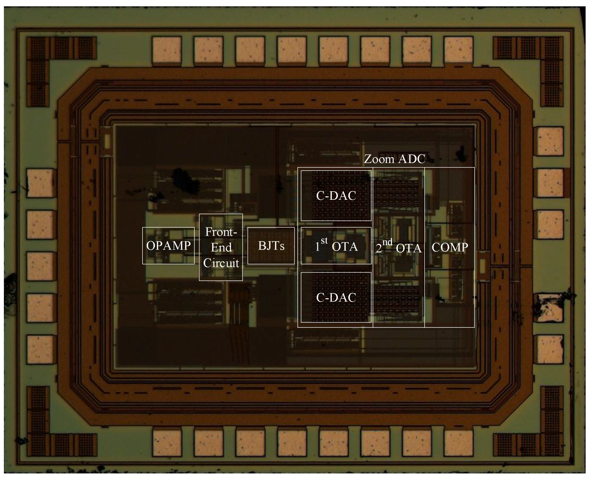
The circuit was implemented in 0.18 μm CMOS technology provided by Semiconductor Manufacturing International Corp. (SMIC, Shanghai, China), and all current sources employed a current of 180 nA. The chip consumed 6.1 μA with a 1.8 V supply voltage, where the current consumption of the front-end circuit was 4.6 μA and the current consumption of the zoom ADC was 1.5 μA. The core area of the chip was 860 μm × 580 μm. A micrograph of the chip is shown in Figure 7.
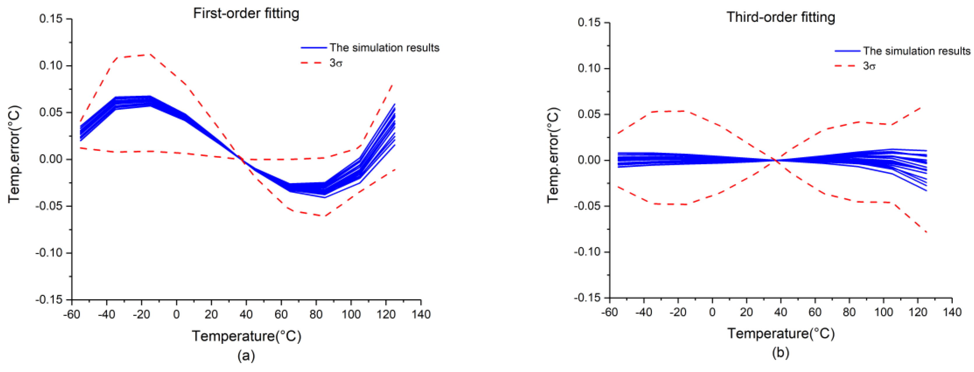
Figure 8 presents the simulation results of the front-end circuit obtained via 20 Monte Carlo simulations. Here, Figure 8a presents the simulation results of the first-order fitting, which exhibits 3σ-inaccuracies of +0.12/−0.06 °C from −55 °C to +125 °C. In addition, Figure 8b presents the simulation results of the third-order fitting, which exhibits 3σ-inaccuracies of ±0.08 °C from −55 °C to +125 °C.
The simulation results of the chip are presented in Figure 9. Here, Figure 9a presents the results of first-order fitting, which exhibits 3σ-inaccuracies of +0.25/−0.13 °C over the temperature range considered. In addition, Figure 9b presents the results of third-order fitting, which exhibits 3σ-inaccuracies of +0.18/−0.13 °C over the temperature range considered.
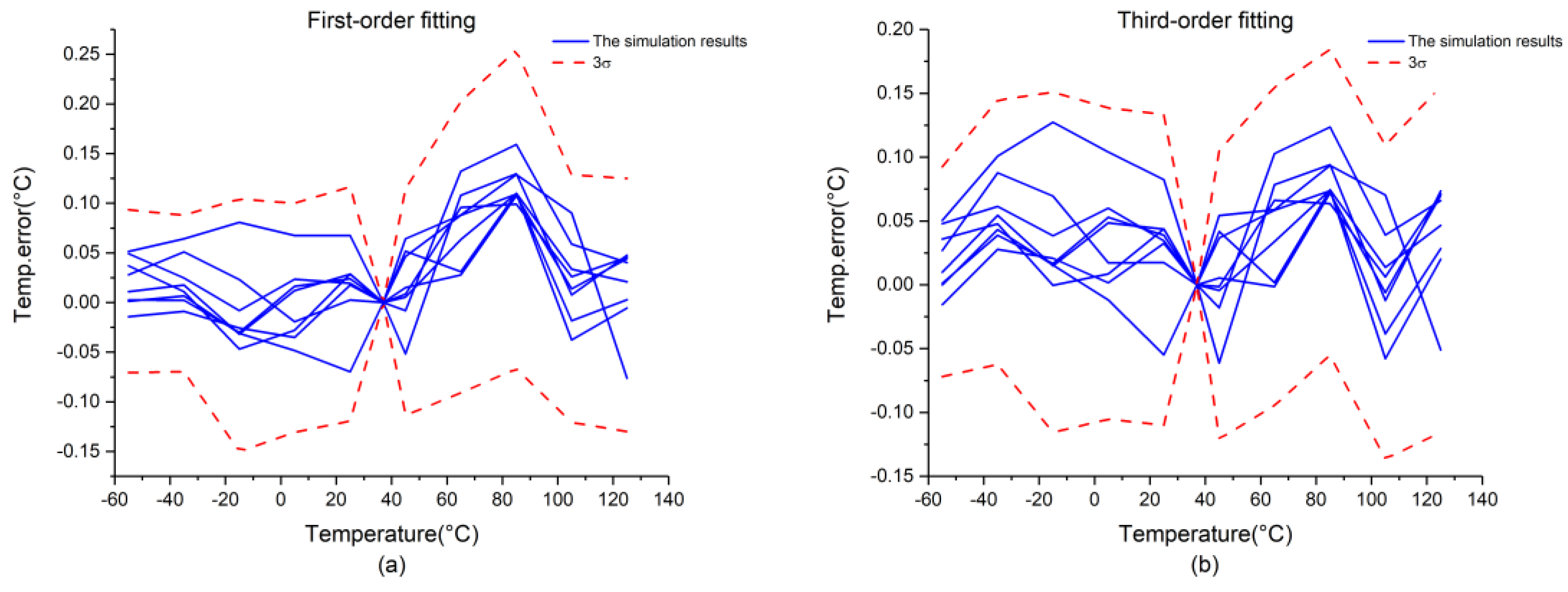
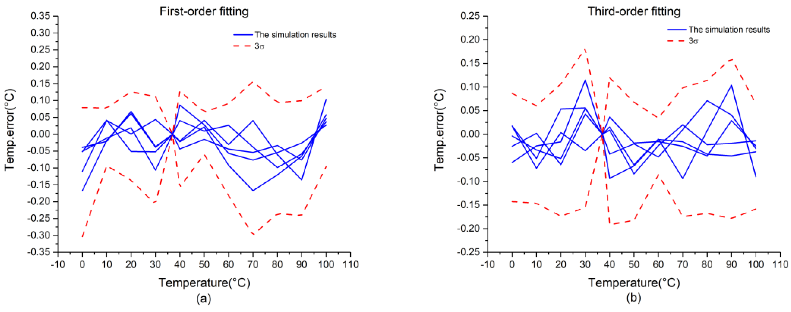
Figure 10 presents the measurement results of the chip. During measurements, we added a shielding box to improve the accuracy of the temperature sensor. As shown in Figure 10a, the chip exhibits 3σ-inaccuracies of +0.15/−0.3 °C from 0 °C to +100 °C with first-order fitting. Figure 10b presents the measurement results of third-order fitting, which shows that the chip can achieve 3σ-inaccuracies of ±0.2 °C from 0 °C to +100 °C.
As demonstrated by the simulation and measurement results, third-order fitting can achieve a greater measurement than first-order fitting. The measured performance of the temperature sensor is compared with the performances of previously reported state-of-the-art temperature sensor implementations in Table 1. Because of the employment of the second-order zoom ADC, the parameter figure-of-merit (FOM) of the sensor is better than those presented in References [6,15], which shows that the proposed sensor provides better resolution and a reduced conversion time. However, the measurement temperature range of this work is only from 0 °C to 100 °C because of the limitations of the measurement equipment. As a result, the Rel.InAcc value of the proposed circuit is 0.4%.
The present work has taken errors into account as much as possible and employs the ALL-DEM approach and calibration to improve the accuracy of the proposed temperature sensor. Among the remaining errors, the curvature error is the largest source of error. Therefore, a curvature calibration or a curvature compensation technology can be expected to improve the accuracies of the temperature sensor. In addition, while the BJT-based temperature sensors provide higher accuracy than thermistor-based sensors, they also require greater power consumption. A higher-order zoom ADC can reduce the power consumption, although its implementation will also require a greater die area. The miniaturization of BJT-based temperature sensors is also an important consideration, and the means of reducing the die area while simultaneously reducing the power consumption of the temperature sensor will be the objective of future research.
7. Conclusions
This paper proposed a low power, energy-efficient precision CMOS temperature sensor circuit implemented in 0.18 μm CMOS technology provided by SMIC. Using the novel ALL-DEM approach, all current sources in the proposed front-end circuit are matched dynamically to reduce system errors arising from current ratio mismatch. Single-point calibration was adopted to improve the accuracy of the sensor. According to the experimental results, the proposed circuit provides a maximum temperature error of ±0.2 °C over the temperature range from 0 °C to +100 °C. The proposed circuit is applicable to a wide range of temperature sensor applications.
Author Contributions
Rongshan Wei provided the initial concepts, prototypes and wrote the paper. Xiaotian Bao conducted the measurement of the temperature sensor and analyzed the data.
Conflicts of Interest
The authors declare no conflict of interest.
References
- Zaliasl, S.; Salvia, J.C.; Hill, G.C.; Chen, L.; Joo, K.; Palwai, R.; Arumugam, N.; Phadke, M.; Mukherjee, S.; Lee, H.C.; et al. A 3 ppm 1.5 × 0.8 mm2 1.0 μA 32.768 kHz MEMS-based oscillator. IEEE J. Solid-State Circuits 2015, 50, 291–302. [Google Scholar] [CrossRef]
- Maderbacher, G.; Marsili, S.; Motz, M.; Jackum, T.; Thielmann, J.; Hassander, H.; Gruber, H.; Hus, F.; Sandner, C. A digitally assisted single-point-calibration CMOS bandgap voltage reference with a 3σ inaccuracy of ±0.08% for fuel-gauge applications. In Proceedings of the 2015 International IEEE ISSCC, San Francisco, CA, USA, 22–26 February 2015; pp. 1–3. [Google Scholar]
- Wu, C.K.; Chan, W.S.; Lin, T.H. A 80 kS/s 36 μW resistor-based temperature sensor using BGR-free SAR ADC with a unevenly-weighted resistor string in 0.18 μm CMOS. In Proceedings of the 2011 Symposium on VLSI Circuits (VLSIC), Honolulu, HI, USA, 15–17 June 2011; pp. 222–223. [Google Scholar]
- Chen, P.; Chen, C.-C.; Tsai, C.-C.; Lu, W.-F. A time-to-digital-converter-based CMOS smart temperature sensor. IEEE J. Solid-State Circuits 2005, 40, 1642–1648. [Google Scholar] [CrossRef]
- Testi, N.; Yang, X. A 0.2 nJ/sample 0.01 mm2 ring oscillator based temperature sensor for on-chip thermal management. In Proceedings of the IEEE International Symposium on Quality Electronic Design, Santa Clara, CA, USA, 4–6 March 2013; pp. 696–702. [Google Scholar]
- Lee, H.-Y.; Hsu, C.-M.; Luo, C.-H. CMOS thermal sensing system with simplified circuits and high accuracy for biomedical application. In Proceedings of the 2006 IEEE International Symposium on Circuits and Systems, Island of Kos, Greece, 21–24 May 2006; pp. 4367–4370. [Google Scholar]
- Aita, A.L.; Pertijs, M.A.P.; Makinwa, K.A.A.; Huijsing, J.H. A CMOS smart temperature sensor with a batch-calibrated inaccuracy of ±0.25 °C (3σ) from −70°C to 130 °C. In Proceedings of the 2009 IEEE International Solid-State Circuits Conference—Digest of Technical Papers, San Francisco, CA, USA, 8–12 February 2009; pp. 342–343. [Google Scholar]
- Souri, K.; Chae, Y.; Makinwa, K.A.A. A CMOS temperature sensor with a voltage-calibrated inaccuracy of ±0.15 °C (3σ) from −55 °C to 125 °C. IEEE J. Solid-State Circuits 2013, 48, 292–301. [Google Scholar] [CrossRef]
- Pertijs, M.A.P.; Makinwa, K.A.A.; Huijsing, J.H. A CMOS smart temperature sensor with a 3σ inaccuracy of ±0.1 °C from −55 °C to 125 °C. IEEE J. Solid-State Circuits 2005, 40, 2805–2815. [Google Scholar] [CrossRef]
- Pertijs, M.A.P.; Niederkorn, A.; Ma, X.; Bakker, A.; Huijsing, J.H. A CMOS smart temperature sensor with a 3σ inaccuracy of ±0.5 °C from −50 °C to 120 °C. IEEE J. Solid-State Circuits 2005, 40, 454–461. [Google Scholar] [CrossRef]
- Souri, K.; Kashmiri, M.; Makinwa, K. A CMOS temperature sensor with an energy-efficient zoom ADC and an Inaccuracy of ±0.25 °C (3σ) from −40 °C to 125 °C. In Proceedings of the IEEE International Solid-State Circuits Conference, San Francisco, CA, USA, 7–11 February 2010; pp. 310–311. [Google Scholar]
- Pertijs, M.A.P.; Huijsing, J. Precision Temperature Sensors in CMOS Technology; Springer: Dordrecht, The Netherlands, 2006. [Google Scholar]
- Souri, K.; Makinwa, K.A.A. A 0.12 mm2 7.4 μW micropower temperature sensor with an inaccuracy of ±0.2 °C (3σ) from −30 °C to 125 °C. IEEE J. Solid-State Circuits 2011, 46, 1693–1700. [Google Scholar] [CrossRef]
- Hastings, A. The Art of Analog Layout; Prentice Hall: Upper Saddle River, NJ, USA, 2006. [Google Scholar]
- Klaassen, K.B. Digitally controlled absolute voltage division. IEEE Trans. Instrum. Meas. 1975, 24, 106–112. [Google Scholar] [CrossRef]
- Van De Plassche, R.J. Dynamic element matching for high-accuracy monolithic D/A converters. IEEE J. Solid-State Circuits 1976, 11, 795–800. [Google Scholar] [CrossRef]
- Yousefzadeh, B.; Shalmany, S.H.; Makinwa, K.A.A. A BJT-Based Temperature-to-Digital Converter with ±60 mK (3σ) Inaccuracy From −55 °C to +125 °C in 0.16-μm CMOS. IEEE J. Solid-State Circuits 2017, 52, 1044–1052. [Google Scholar] [CrossRef]
- Heidary, A.; Wang, G.; Makinwa, K.; Meijer, G. 12.8 A BJT-based CMOS temperature sensor with a 3.6pJ·K2-resolution FoM. In Proceedings of the 2014 IEEE International Solid-State Circuits Conference Digest of Technical Papers (ISSCC), San Francisco, CA, USA, 9–13 February 2014; pp. 224–225. [Google Scholar]
Figure 1.
Conventional bipolar junction transistor (BJT) based temperature sensor front-end circuit.
Figure 1.
Conventional bipolar junction transistor (BJT) based temperature sensor front-end circuit.

Figure 2.
Operating principles of analog-to-digital converters (ADCs): (a) sigma-delta ADC; (b) zoom ADC.
Figure 2.
Operating principles of analog-to-digital converters (ADCs): (a) sigma-delta ADC; (b) zoom ADC.

Figure 3.
Front-end circuit employing the all dynamic element matching (ALL-DEM) approach.

Figure 4.
Maximum temperature errors simulations with different dynamic element matching (DEM) schemes.
Figure 4.
Maximum temperature errors simulations with different dynamic element matching (DEM) schemes.

Figure 5.
Structure of the zoom ADC. (Note: SAR: successive approximation; LSB: least significant bit; MSB: most significant bit; DAC: digital-to-analog converter).
Figure 5.
Structure of the zoom ADC. (Note: SAR: successive approximation; LSB: least significant bit; MSB: most significant bit; DAC: digital-to-analog converter).

Figure 6.
Overview of the temperature sensor.

Figure 7.
Chip micrograph. (Note: OTA: operational transconductance amplifier; C-DAC: capacitive digital-to-analog converter; COMP: comparator).
Figure 7.
Chip micrograph. (Note: OTA: operational transconductance amplifier; C-DAC: capacitive digital-to-analog converter; COMP: comparator).

Figure 8.
Simulation results of the front-end circuit: (a) first-order fitting; (b) third-order fitting.
Figure 8.
Simulation results of the front-end circuit: (a) first-order fitting; (b) third-order fitting.

Figure 9.
Simulation results for the chip: (a) first-order fitting; (b) third-order fitting.

Figure 10.
Measurement results of the chip: (a) first-order fitting; (b) third-order fitting.


Table 1.
Performance Comparison with Previously Reported Temperature Sensor Schemes.
| Item | [8] | [9] | [17] | [18] | This Work |
|---|---|---|---|---|---|
| Year | 2013 | 2005 | 2017 | 2014 | 2018 |
| Process (μm) | 0.16 | 0.7 | 0.16 | 0.7 | 0.18 |
| Area (mm2) | 0.08 | 4.5 | 0.16 | 0.8 | 0.5 |
| VDD (V) | 1.5–2 | 2.5–5.5 | 1.5–2 | 2.9–5.5 | 1.8 |
| Supply Current (μA) | 3.4 | 75 | 4.6 | 55 | 6.1 |
| Temperature Range (°C) | −55 to +125 | −55 to +125 | −55 to +125 | −45 to +130 | 0 to +100 |
| Resolution (°C) Tconv (ms) | 0.02 (5.3) | 0.01 (100) | 0.015 (5) | 0.003 (2.2) | 0.01 (3.4) |
| Inaccuracy (°C) | ±0.15 | ±0.1 | ±0.06 | ±0.15 | ±0.2 |
| FOM * (pJ°C2) | 11 | 1875 | 7.8 | 3.2 | 3.8 |
| Rel.InAcc. ** (%) | 0.17 | 0.11 | 0.07 | 0.17 | 0.4 |
* FOM = (Power·Tconv) × (Resolution)2. ** Rel.InAcc = (2 × Inaccuracy/Range) × 100%.
© 2018 by the authors. Licensee MDPI, Basel, Switzerland. This article is an open access article distributed under the terms and conditions of the Creative Commons Attribution (CC BY) license (http://creativecommons.org/licenses/by/4.0/).
Share and Cite
MDPI and ACS Style
Wei, R.; Bao, X. A Low Power Energy-Efficient Precision CMOS Temperature Sensor †. Micromachines 2018, 9, 257. https://doi.org/10.3390/mi9060257
AMA Style
Wei R, Bao X. A Low Power Energy-Efficient Precision CMOS Temperature Sensor †. Micromachines. 2018; 9(6):257. https://doi.org/10.3390/mi9060257
Chicago/Turabian StyleWei, Rongshan, and Xiaotian Bao. 2018. "A Low Power Energy-Efficient Precision CMOS Temperature Sensor †" Micromachines 9, no. 6: 257. https://doi.org/10.3390/mi9060257
Note that from the first issue of 2016, this journal uses article numbers instead of page numbers. See further details here.