Low-Cost, Accessible Fabrication Methods for Microfluidics Research in Low-Resource Settings

 , and
, and 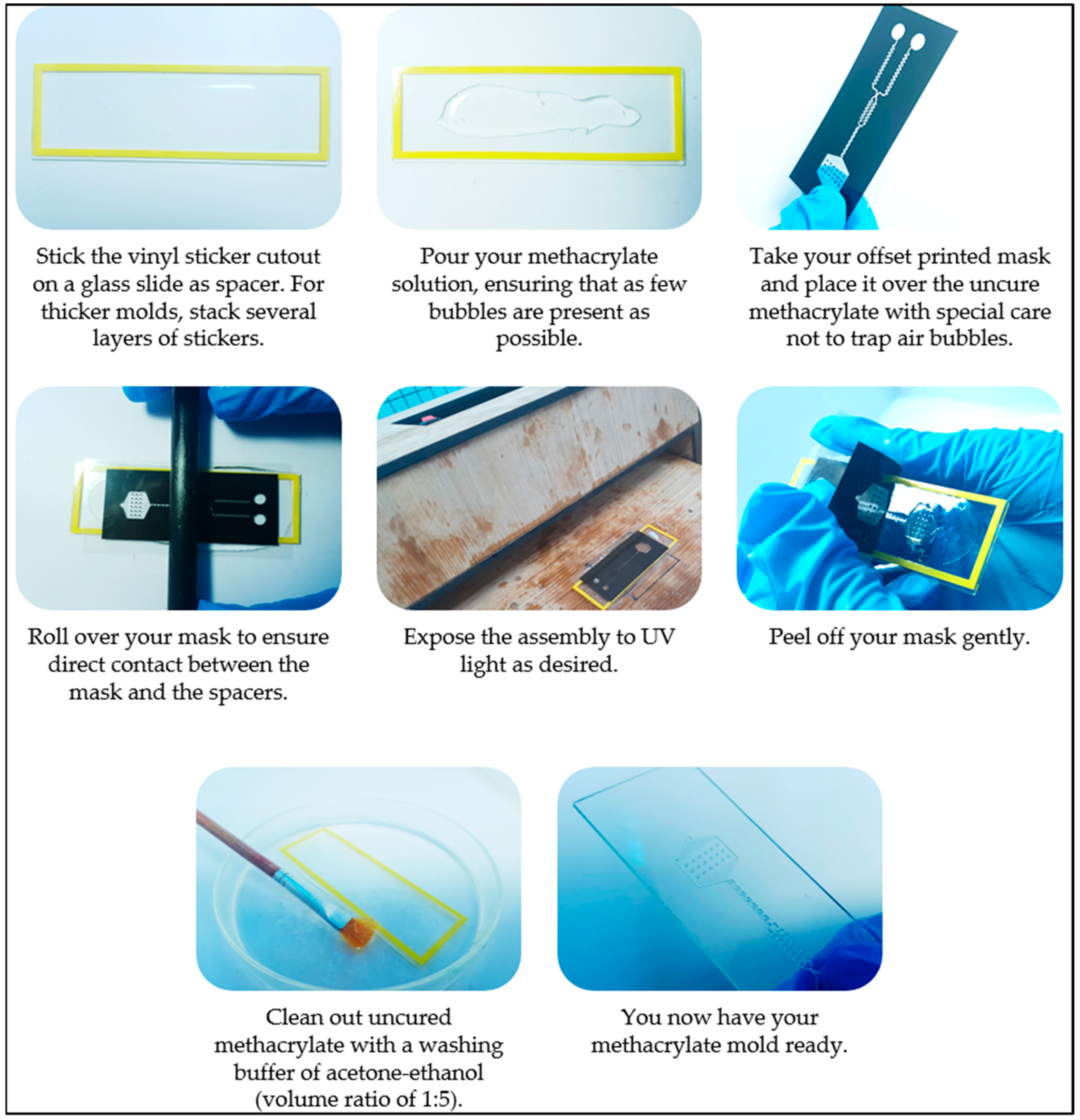
Abstract
:1. Introduction
2. Materials and Methods
2.1. Photomask Fabrication
2.2. Photolithography Process
2.2.1. Methacrylate Coating
2.2.2. UV Exposure
2.2.3. Washing
2.3. Molding Microfluidic Chips
2.3.1. Soft Lithography
2.3.2. Soft Embossing
3. Results
3.1. Alternative to the Photomask
3.2. Alternative to the Mask Aligner and Hg-Vapor Lamp
3.3. Alternative to Spin Coating
3.4. Compatibility with Microfluidics Fabrication Methods
4. Conclusions
Author Contributions
Funding
Acknowledgments
Conflicts of Interest
References
- Sharma, H.; Nguyen, D.; Chen, A.; Lew, V.; Khine, M. Unconventional low-cost fabrication and patterning techniques for point of care diagnostics. Ann. Biomed. Eng. 2011, 39, 1313–1327. [Google Scholar] [CrossRef] [PubMed]
- Nie, Z.; Kumacheva, E. Patterning surfaces with functional polymers. Nat. Mater. 2008, 7, 277–290. [Google Scholar] [CrossRef] [PubMed]
- Taylor, D.; Dyer, D.; Lew, V.; Khine, M. Shrink film patterning by craft cutter: complete plastic chips with high resolution/high-aspect ratio channel. Lab Chip 2010, 10, 2472. [Google Scholar] [CrossRef] [PubMed]
- Yuen, P.K.; Goral, V.N. Low-cost rapid prototyping of flexible microfluidic devices using a desktop digital craft cutter. Lab Chip 2010, 10, 384–387. [Google Scholar] [CrossRef] [PubMed]
- Wang, W.; Zhao, S.; Pan, T. Lab-on-a-print: from a single polymer film to three-dimensional integrated microfluidics. Lab Chip 2009, 9, 1133. [Google Scholar] [CrossRef] [PubMed]
- Sollier, K.; Mandon, C.A.; Heyries, K.A.; Blum, L.J.; Marquette, C.A. “Print-n-Shrink” technology for the rapid production of microfluidic chips and protein microarrays. Lab Chip 2009, 9, 3489. [Google Scholar] [CrossRef] [PubMed]
- Grimes, A.; Breslauer, D.N.; Long, M.; Pegan, J.; Lee, L.P.; Khine, M. Shrinky-Dink microfluidics: rapid generation of deep and rounded patterns. Lab Chip 2008, 8, 170–172. [Google Scholar] [CrossRef] [PubMed] [Green Version]
- Piccin, E.; Ferraro, D.; Sartori, P.; Chiarello, E.; Pierno, M.; Mistura, G. Generation of water-in-oil and oil-in-water microdroplets in polyester-toner microfluidic devices. Sens. Actuators B Chem. 2014, 196, 525–531. [Google Scholar] [CrossRef] [Green Version]
- Mao, X.; Huang, T.J. Microfluidic diagnostics for the developing world. Lab Chip 2012, 12, 1412–1416. [Google Scholar] [CrossRef] [PubMed]
- Bartolo, D.; Degré, G.; Nghe, P.; Studer, V. Microfluidic stickers. Lab Chip 2008, 8, 274–279. [Google Scholar] [CrossRef] [PubMed]
- Silvestrini, S.; Ferraro, D.; Tóth, T.; Pierno, M.; Carofiglio, T.; Mistura, G.; Maggini, M. Tailoring the wetting properties of thiolene microfluidic materials. Lab Chip 2012, 12, 4041–4043. [Google Scholar] [CrossRef] [PubMed]
- Waldbaur, A.; Rapp, H.; Länge, K.; Rapp, B.E. Let there be chip—towards rapid prototyping of microfluidic devices: one-step manufacturing processes. Anal. Methods 2011, 3, 2681. [Google Scholar] [CrossRef]
- Kamei, K.; Mashimo, Y.; Koyama, Y.; Fockenberg, C.; Nakashima, M.; Nakajima, M.; Li, J.; Chen, Y. 3D printing of soft lithography mold for rapid production of polydimethylsiloxane-based microfluidic devices for cell stimulation with concentration gradients. Biomed. Microdevices 2015, 17, 36. [Google Scholar] [CrossRef] [PubMed]
- Ferraro, D.; Serra, M.; Ferrante, I.; Viovy, J.-L.; Descroix, S. Microfluidic valve with zero dead volume and negligible back-flow for droplets handling. Sens. Actuators B Chem. 2018, 258, 1051–1059. [Google Scholar] [CrossRef]
- Bhattacharjee, N.; Urrios, A.; Kang, S.; Folch, A. The upcoming 3D-printing revolution in microfluidics. Lab Chip 2016, 16, 1720–1742. [Google Scholar] [CrossRef] [PubMed] [Green Version]
- Waheed, S.; Cabot, J.M.; Macdonald, N.P.; Lewis, T.; Guijt, R.M.; Paull, B.; Breadmore, M.C. 3D printed microfluidic devices: enablers and barriers. Lab Chip 2016, 16, 1993–2013. [Google Scholar] [CrossRef] [PubMed] [Green Version]
- Li, Y.; Wu, P.; Luo, Z.; Ren, Y.; Liao, M.; Feng, L.; Li, Y.; He, L. Rapid fabrication of microfluidic chips based on the simplest LED lithography. J. Micromech. Microeng. 2015, 25, 055020. [Google Scholar] [CrossRef]
- Chen, Y.; Zhang, L.; Chen, G. Fabrication, modification, and application of poly(methyl methacrylate) microfluidic chips. Electrophoresis 2008, 29, 1801–1814. [Google Scholar] [CrossRef] [PubMed]
- McDonald, J.C.; Duffy, D.C.; Anderson, J.R.; Chiu, D.T.; Wu, H.; Schueller, O.J.A.; Whitesides, G.M. Fabrication of microfluidic systems in poly(dimethylsiloxane). Electrophoresis 2000, 21, 27–40. [Google Scholar] [CrossRef]
- Toepke, M.W.; Beebe, D.J. PDMS absorption of small molecules and consequences in microfluidic applications. Lab Chip 2006, 6, 1484–1486. [Google Scholar] [CrossRef] [PubMed]
- Wang, J.D.; Douville, N.J.; Takayama, S.; ElSayed, M. Quantitative Analysis of Molecular Absorption into PDMS Microfluidic Channels. Ann. Biomed. Eng. 2012, 40, 1862–1873. [Google Scholar] [CrossRef] [PubMed]
- Tsao, C.-W. Polymer Microfluidics: Simple, Low-Cost Fabrication Process Bridging Academic Lab Research to Commercialized Production. Micromachines 2016, 7, 225. [Google Scholar] [CrossRef]
- Halldorsson, S.; Lucumi, E.; Gómez-Sjöberg, R.; Fleming, R.M.T. Advantages and challenges of microfluidic cell culture in polydimethylsiloxane devices. Biosens. Bioelectron. 2015, 63, 218–231. [Google Scholar] [CrossRef] [PubMed]
- Mukhopadhyay, R. When PDMS isn’t the best. Anal. Chem. 2007, 79, 3248–3253. [Google Scholar] [CrossRef] [PubMed]
- Gratton, S.E.A.; Williams, S.S.; Napier, M.E.; Pohlhaus, P.D.; Zhou, Z.; Wiles, K.B.; Maynor, B.W.; Shen, C.; Olafsen, T.; Samulski, E.T.; DeSimone, J.M. The Pursuit of a Scalable Nanofabrication Platform for Use in Material and Life Science Applications. Acc. Chem. Res. 2008, 41, 1685–1695. [Google Scholar] [CrossRef] [PubMed] [Green Version]
- Lachaux, J.; Alcaine, C.; Gómez-Escoda, B.; Perrault, C.M.; Duplan, D.O.; Wu, P.-Y.J.; Ochoa, I.; Fernandez, L.; Mercier, O.; Coudreuse, D.; Roy, E. Thermoplastic elastomer with advanced hydrophilization and bonding performances for rapid (30 s) and easy molding of microfluidic devices. Lab Chip 2017, 17. [Google Scholar] [CrossRef] [PubMed]
- Ahmadzadeh, F.; Tsai, S.S.H.; Papini, M. Effect of curing parameters and configuration on the efficacy of ultraviolet light curing self-adhesive masks used for abrasive jet micro-machining. Precis. Eng. 2017, 49, 354–364. [Google Scholar] [CrossRef]
- Huntington, M.D.; Odom, T.W. A Portable, Benchtop Photolithography System Based on a Solid-State Light Source. Small 2011, 7, 3144–3147. [Google Scholar] [CrossRef] [PubMed]
- Serra, M.; Pereiro, I.; Yamada, A.; Viovy, J.-L.; Descroix, S.; Ferraro, D. A simple and low-cost chip bonding solution for high pressure, high temperature and biological applications. Lab Chip 2017, 17, 629–634. [Google Scholar] [CrossRef] [PubMed] [Green Version]
- Wu, H.; Huang, B.; Zare, R.N. Construction of microfluidic chips using polydimethylsiloxane for adhesive bonding. Lab Chip 2005, 5, 1393. [Google Scholar] [CrossRef] [PubMed]


© 2018 by the authors. Licensee MDPI, Basel, Switzerland. This article is an open access article distributed under the terms and conditions of the Creative Commons Attribution (CC BY) license (http://creativecommons.org/licenses/by/4.0/).
Share and Cite
Nguyen, H.-T.; Thach, H.; Roy, E.; Huynh, K.; Perrault, C.M.-T. Low-Cost, Accessible Fabrication Methods for Microfluidics Research in Low-Resource Settings. Micromachines 2018, 9, 461. https://doi.org/10.3390/mi9090461
Nguyen H-T, Thach H, Roy E, Huynh K, Perrault CM-T. Low-Cost, Accessible Fabrication Methods for Microfluidics Research in Low-Resource Settings. Micromachines. 2018; 9(9):461. https://doi.org/10.3390/mi9090461
Chicago/Turabian StyleNguyen, Hoang-Tuan, Ha Thach, Emmanuel Roy, Khon Huynh, and Cecile Mong-Tu Perrault. 2018. "Low-Cost, Accessible Fabrication Methods for Microfluidics Research in Low-Resource Settings" Micromachines 9, no. 9: 461. https://doi.org/10.3390/mi9090461
APA StyleNguyen, H.-T., Thach, H., Roy, E., Huynh, K., & Perrault, C. M.-T. (2018). Low-Cost, Accessible Fabrication Methods for Microfluidics Research in Low-Resource Settings. Micromachines, 9(9), 461. https://doi.org/10.3390/mi9090461