LED Optrode with Integrated Temperature Sensing for Optogenetics

 , , , , , , , and
Abstract
:1. Introduction
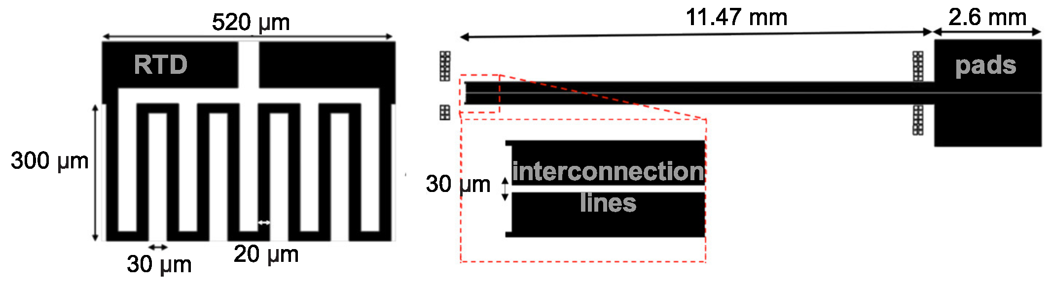
2. Probe Design
3. Methods
3.1. Microfabrication
3.2. Characterization
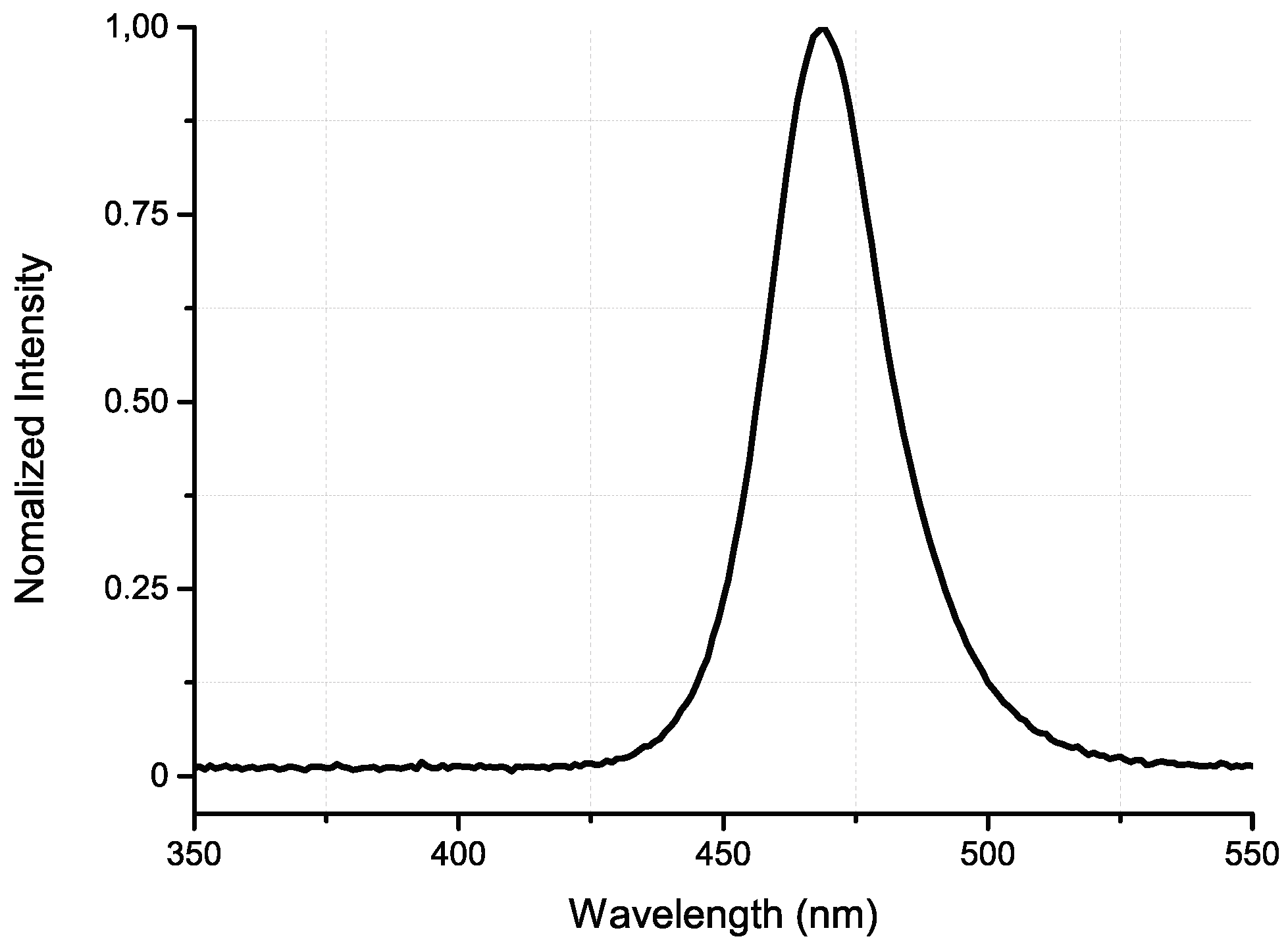
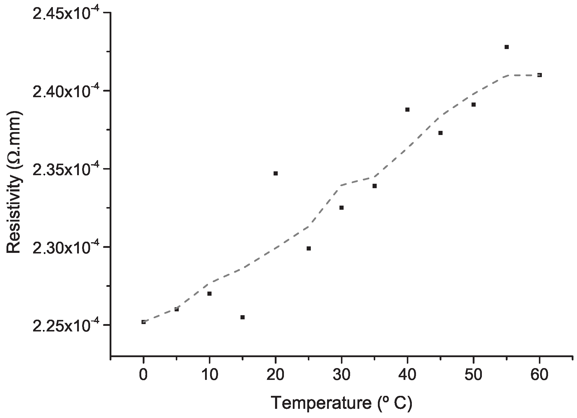
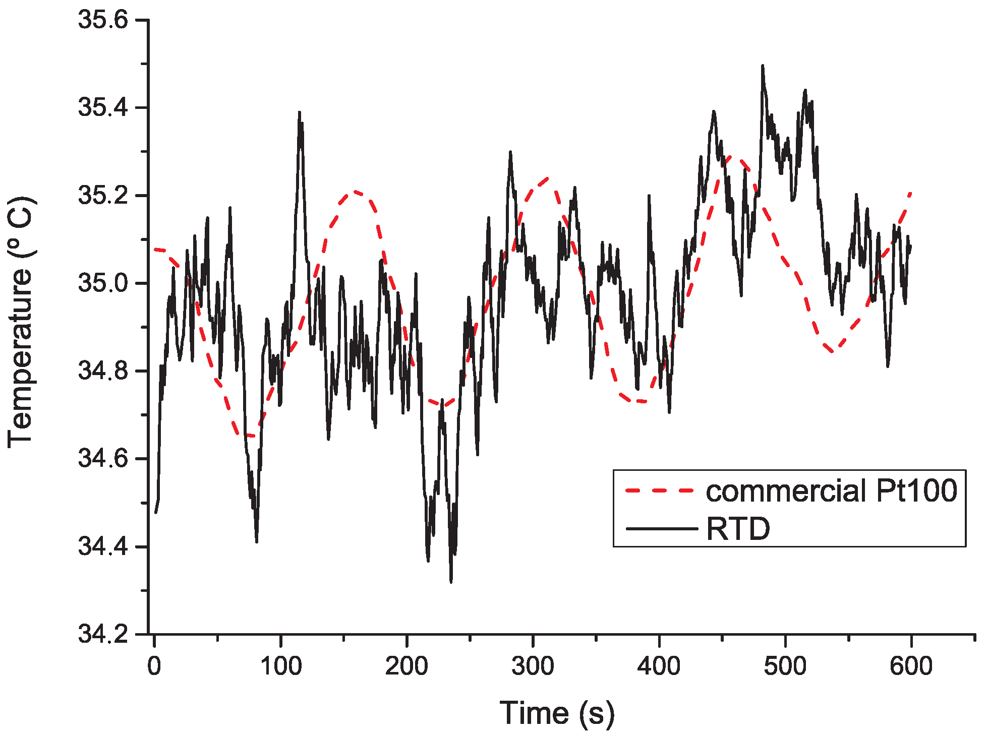
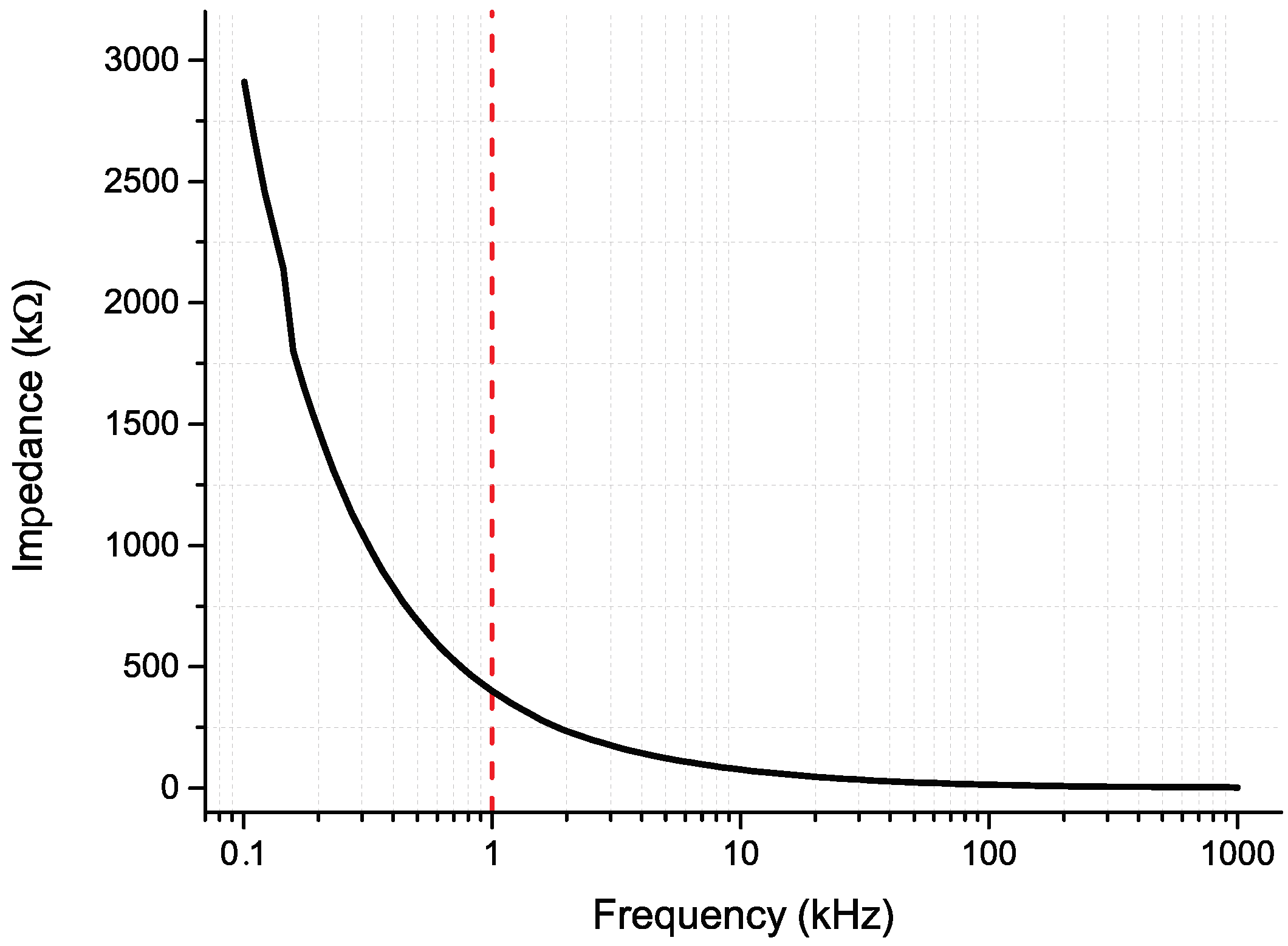
4. Results and Discussion
5. Conclusions
Author Contributions
Acknowledgments
Conflicts of Interest
Abbreviations
| RTD | Resistance Temperature Detector |
| e-beam | Electron-Beam |
| EIS | Electrochemical Impedance Spectroscopy |
| UV | Ultraviolet |
| DI | Deionized |
| TCR | Temperature Coefficient of Resistance |
| CMOS | Complementary Metal-Oxide-Semiconductor |
| RF | Radio-Frequency |
| DC | Direct Current |
| AC | Alternating Current |
References
- Maharbiz, M.M.; Muller, R.; Alon, E.; Rabaey, J.M.; Carmena, J.M. Reliable Next-Generation Cortical Interfaces for Chronic Brain–Machine Interfaces and Neuroscience. Proc. IEEE 2017, 105, 73–82. [Google Scholar] [CrossRef]
- Deisseroth, K. Optogenetics: 10 years of microbial opsins in neuroscience. Nat. Neurosci. 2015, 18, 1213–1225. [Google Scholar] [CrossRef] [PubMed] [Green Version]
- Boyden, E.S.; Zhang, F.; Bamberg, E.; Nagel, G.; Deisseroth, K. Millisecond-timescale, genetically targeted optical control of neural activity. Nat. Neurosci. 2005, 8, 1263–1268. [Google Scholar] [CrossRef] [PubMed]
- Goncalves, S.B.; Ribeiro, J.F.; Silva, A.F.; Costa, R.M.; Correia, J.H. Design and Manufacturing Challenges of Optogenetic Neural Interfaces: A Review. J. Neural Eng. 2017, 14, 041001. [Google Scholar] [CrossRef] [PubMed]
- Wu, F.; Stark, E.; Ku, P.; Wise, K.D.; Buzsáki, G.; Yoon, E. Monolithically Integrated μLEDs on Silicon Neural Probes for High-Resolution Optogenetic Studies in Behaving Animals. Neuron 2015, 88, 1136–1148. [Google Scholar] [CrossRef] [PubMed]
- Scharf, R.; Tsunematsu, T.; McAlinden, N.; Dawson, M.D.; Sakata, S.; Mathieson, K. Depth-specific optogenetic control in vivo with a scalable, high-density μLED neural probe. Nat. Sci. Rep. 2016, 8, 28381. [Google Scholar] [CrossRef] [PubMed] [Green Version]
- Kwon, K.Y.; Sirowatka, B.; Weber, A.; Li, W. Opto-μEcoG Array: A Hybrid Neural Interface With Transparent μEcoG Electrode Array and Integrated LEDs for Optogenetics. IEEE Trans. Biomed. Circuits Syst. 2013, 7, 593–600. [Google Scholar] [CrossRef] [PubMed]
- Cao, H.; Gu, L.; Mohanty, S.K.; Chiao, J.C. An Integrated μ-LED Optrode for Optogenetic Stimulation and Electrical Recording. IEEE Trans. Biomed. Eng. 2013, 60, 225–229. [Google Scholar] [CrossRef] [PubMed]
- Ayub, S.; Gossler, C.; Schwaerzle, M.; Klein, E.; Paul, O.; Schwarz, U.T.; Ruther, P. High-Density Probe with Integrated Thin-Film Micro Light Emitting Diodes (μ-LEDs) For Optogenetic Applications. In Proceedings of the 2016 IEEE 29th International Conference on Micro Electro Mechanical Systems (MEMS), Shanghai, China, 24–28 January 2016; pp. 379–382. [Google Scholar]
- Goßler, C.; Bierbrauer, C.; Moser, R.; Kunzer, M.; Holc, K.; Pletschen, W.; Köhler, K.; Wagner, J.; Schwaerzle, M.; Ruther, P.; et al. GaN-based micro-LED arrays on flexible substrates for optical cochlear implants. J. Phys. D Appl. Phys. 2014, 47, 205401. [Google Scholar] [CrossRef]
- Alt, M.T.; Fiedler, E.; Rudmann, L.; Ordonez, J.S.; Ruther, P.; Stieglitz, T. Let There Be Light—Optoprobes for Neural Implants. Proc. IEEE 2017, 105, 101–138. [Google Scholar] [CrossRef]
- Wang, H.; Wang, B.; Normoyle, K.P.; Jackson, K.; Spitler, K.; Sharrock, M.F.; Miller, C.M.; Best, C.; Llano, D.; Du, R. Brain temperature and its fundamental properties: A review for clinical neuroscientists. Front. Neurosci. 2014, 8, 307. [Google Scholar] [CrossRef] [PubMed] [Green Version]
- Kiyatkin, E.A. Brain Hyperthermia During Physiological and Pathological Conditions: Causes, Mechanisms, and Functional Implications. Curr. Neurovasc. Res. 2004, 1, 77–90. [Google Scholar] [CrossRef]
- Haveman, J.; Sminia, P.; Wondergem, J.; van der Zee, J.; Hulshof, M.C. Effects of hyperthermia on the central nervous system: What was learnt from animal studies? Int. J. Hyperth. 2005, 21, 473–487. [Google Scholar] [CrossRef] [PubMed]
- Childs, C. Human brain temperature: Regulation, measurement and relationship with cerebral trauma: Part 1. Br. J. Neurosurg. 2008, 22, 486–496. [Google Scholar] [CrossRef] [PubMed]
- Kim, S.; Tathireddy, P.; Normann, R.A.; Solzbacher, F. In vitro and in vivo study of temperature increases in the brain due to a neural implant. In Proceedings of the 2007 3rd International IEEE/EMBS Conference on Neural Engineering, Kohala Coast, HI, USA, 2–5 May 2007; pp. 163–166. [Google Scholar]
- McAlinden, N.; Massoubre, D.; Richardson, E.; Gu, E.; Sakata, S.; Dawson, M.D.; Mathieson, K. Thermal and optical characterization of micro-LED probes for in vivo optogenetic neural stimulation. Opt. Lett. 2013, 38, 992–994. [Google Scholar] [CrossRef] [PubMed]
- Dong, N.; Berlinguer-Palmini, R.; Soltan, A.; Ponon, N.; O’Neil, A.; Travelyan, A.; Maaskant, P.; Degenaar, P.; Sun, X. Opto-electro-thermal optimization of photonic probes for optogenetic neural stimulation. J. Biophotonics 2018, 30, e201700358. [Google Scholar] [CrossRef] [PubMed]
- Li, C.; Wu, P.M.; Hartings, J.A.; Wu, Z.; Cheyuo, C.; Wang, P.; LeDoux, D.; Shutter, L.A.; Ramaswamy, B.R.; Ahn, C.H.; et al. Micromachined lab-on-a-tube sensors for simultaneous brain temperature and cerebral blood flow measurements. Biomed. Microdevices 2012, 14, 759–768. [Google Scholar] [CrossRef] [PubMed]
- Li, K.S.; Chao, T.Y.; Cheng, Y.T.; Chen, J.K.; Chen, Y.S. Temperature sensing probe integrated with an SU-8 flexible ribbon cable for heart surgery application. In Proceedings of the 2011 16th International Solid-State Sensors, Actuators and Microsystems Conference, Beijing, China, 5–9 June 2011; pp. 2180–2183. [Google Scholar]
- Wu, Z.; Li, C.; Hartings, J.; Narayan, R.K.; Ahn, C. Polysilicon-based flexible temperature sensor for brain monitoring with high spatial resolution. J. Micromech. Microeng. 2016, 27, 025001. [Google Scholar] [CrossRef] [Green Version]
- Kim, T.I.; McCall, J.G.; Jung, Y.H.; Huang, X.; Siuda, E.R.; Li, Y.; Song, J.; Song, Y.M.; Pao, H.A.; Kim, R.H.; et al. Injectable, Cellular- Scale Optoelectronics with Applications for Wireless Optogenetics. Science 2013, 340, 211–216. [Google Scholar] [CrossRef] [PubMed]
- Lee, B.C.; Lim, Y.G.; Kim, K.H.; Lee, S.; Moon, S. Microfabricated neural thermocouple arrays probe for brain research. In Proceedings of the 2009 International Solid-State Sensors, Actuators and Microsystems Conference, Denver, CO, USA, 21–25 June 2009; pp. 338–341. [Google Scholar]
- Fekete, Z.; Csernai, M.; Kocsis, K.; Horváth, A.C.; Pongrácz, A.; Barthó, P. Simultaneous in vivo recording of local brain temperature and electrophysiological signals with a novel neural probe. J. Neural Eng. 2017, 14, 34001. [Google Scholar] [CrossRef] [PubMed]
- Billard, M.W.; Basantani, H.A.; Horn, M.W.; Gluckman, B.J.A. Flexible Vanadium Oxide Thermistor Array for Localized Temperature Field Measurements in Brain. IEEE Sens. J. 2016, 16, 2211–2212. [Google Scholar] [CrossRef]
- Innovative Sensor Technology, I.S.T.A.G. Temperature Sensors. Available online: https://wwwist-agcom/en/products-services/temperature-sensors (accessed on 22 March 2018).
- Galvin, I.M.; Levy, R.; Boyd, J.G.; Day, A.G.; Wallace, M.C. Cooling for cerebral protection during brain surgery. Cochrane Database Syst. Rev. 2015, 1, CD006638. [Google Scholar] [CrossRef] [PubMed]
- Mailly, F.; Giani, A.; Bonnot, R.; Delannoy, F.; Foucaran, A.; Boyer, A. Anemometer with hot platinum thin film. Sens. Actuators A Phys. 2001, 94, 32–38. [Google Scholar] [CrossRef]
- Zribi, A.; Barthès, M.; Bègot, S.; Lanzetta, F.; Rauch, J.Y.; Moutarlier, V. Design, fabrication and characterization of thin film resistances for heat flux sensing application. Sens. Actuators A Phys. 2016, 245, 26–39. [Google Scholar] [CrossRef]
- Aslam, M.; Hatfield, J.V. Fabrication of thin film microheater for gas sensors on polyimide membrane. Proc. IEEE Sens. 2003, 1, 389–392. [Google Scholar] [CrossRef]
- Chang, C.; Chiou, J. Development of a Three Dimensional Neural Sensing Device by a Stacking Method. Sensors 2010, 2010 10, 4238–4252. [Google Scholar] [CrossRef]
- Disco Electroformed Bond Blades: NBC-Zseries. Available online: https://www.disco.co.jp/eg/products/catalog/pdf/nbcz.pdf (accessed on 7 August 2018).
- Dean, R.N.; Luque, A. Applications of Microelectromechanical Systems in Industrial Processes and Services. IEEE Trans. Ind. Electron. 2009, 56, 913–925. [Google Scholar] [CrossRef]
- Vieira, E.M.F.; Ribeiro, J.F.; Sousa, R.; Silva, M.M.; Dupont, L.; Goncalves, L.M. Titanium Oxide Adhesion Layer for High Temperature Annealed Si/Si3N4/TiOx/Pt/LiCoO2 Battery Structures. J. Electron. Mater. 2016, 45, 910–916. [Google Scholar] [CrossRef]
- Goncalves, S.B.; Ribeiro, J.F.; Silva, A.F.; Correia, J.H. High Aspect Ratio Neural Probe using conventional Blade Dicing. J. Phys. Conf. Ser. 2016, 757, 012011. [Google Scholar] [CrossRef]
- Chang, B.Y.; Park, S.M. Electrochemical Impedance Spectroscopy. Annu. Rev. Anal. Chem. 2010, 3, 207–229. [Google Scholar] [CrossRef] [PubMed]
- Iles, G.S.; Tindall, R.F. A Thick Film Platinum Resistance Thermometer. Platin. Met. Rev. 1975, 19, 42–47. [Google Scholar]
- Van der Pauw, L.J. A Method of Measuring the Resistivity Hall Coefficient on Lamellae of Arbitrary Shape. Philips Tech. Rev. 1958, 20, 220–224. [Google Scholar] [CrossRef]
- Moser, E.; Mathiesen, I.; Andersen, P. Association between brain temperature and dentate field potentials in exploring and swimming rats. Science 1993, 259, 1324–1326. [Google Scholar] [CrossRef] [PubMed]
- Mcalinden, N.; Gu, E.; Dawson, M.D.; Sakata, S.; Mathieson, K. Optogenetic activation of neocortical neurons in vivo with a sapphire-based micro-scale LED probe. Front. Neural Circuits 2015, 9, 25. [Google Scholar] [CrossRef] [PubMed]
- Ayub, S.; Gentet, L.J.; Fiaáth, R.; Schwaerzle, M.; Borel, M.; David, F.; Barthó, P.; Ulbert, I.; Paul, O.; Ruther, P. Hybrid intracerebral probe with integrated bare LED chips for optogenetic studies. Biomed. Microdevices 2017, 19, 49. [Google Scholar] [CrossRef] [PubMed] [Green Version]
- Jensen, W.; Yoshida, K.; Hofmann, U.G. In-Vivo Implant Mechanics of Flexible, Silicon-Based ACREO Microelectrode Arrays in Rat Cerebral Cortex. IEEE Trans. Biomed. Eng. 2006, 53, 934–940. [Google Scholar] [CrossRef] [PubMed]
- Han, M.; Manoonkitiwongsa, P.S.; Wang, C.X.; McCreery, D.B. In Vivo Validation of Custom-Designed Silicon-Based Microelectrode Arrays for Long-Term Neural Recording and Stimulation. IEEE Trans. Biomed. Eng. 2012, 59, 346–354. [Google Scholar] [CrossRef] [PubMed] [Green Version]
- Sharp, A.A.; Ortega, A.M.; Restrepo, D.; Curran-Everett, D.; Gall, K. In Vivo Penetration Mechanics and Mechanical Properties of Mouse Brain Tissue at Micrometer Scales. IEEE Trans. Biomed. Eng. 2009, 56, 45–53. [Google Scholar] [CrossRef] [PubMed] [Green Version]
- Lopez, C.M.; Putzeys, J.; Raducanu, B.C.; Ballini, M.; Wang, S.; Andrei, A.; Rochus, V.; Vandebriel, R.; Severi, S.; Hoof, C.; et al. A Neural Probe With Up to 966 Electrodes and Up to 384 Configurable Channels in 0.13 μm SOI CMOS. IEEE Trans. Biomed. Eng. 2017, 11, 510–522. [Google Scholar] [CrossRef]
- Scholvin, J.; Kinney, J.P.; Bernstein, J.G.; Moore-Kochlacs, C.; Kopell, N.; Fonstad, C.G.; Boyden, E.S. Close-Packed Silicon Microelectrodes for Scalable Spatially Oversampled Neural Recording. IEEE Trans. Biomed. Eng. 2016, 63, 120–130. [Google Scholar] [CrossRef] [PubMed] [Green Version]
- Raducanu, B.C.; Yazicioglu, R.F.; Lopez, C.M.; Ballini, M.; Putzeys, J.; Wang, S.; Andrei, A.; Rochus, V.; Welkenhuysen, M.; Helleputte, N.V.; et al. Time Multiplexed Active Neural Probe with 1356 Parallel Recording Sites. Sensors 2017, 17, 2388. [Google Scholar] [CrossRef] [PubMed]
- Negi, S.; Bhandari, R.; Rieth, L.; Solzbacher, F. In vitro comparison of sputtered iridium oxide and platinum-coated neural implantable microelectrode arrays. Biomed. Mater. 2010, 5, 015007. [Google Scholar] [CrossRef] [PubMed]
- Xiao, S.Y.; Che, L.F.; Li, X.X.; Wang, Y.L. A novel fabrication process of MEMS devices on polyimide flexible substrates. Microelectron. Eng. 2008, 85, 452–457. [Google Scholar] [CrossRef]
- Fiedler, E.; Cruz, M.F.; Monjara, O.F.; Stieglitz, T.; Member, S. Evaluation of Thin-film Temperature Sensors for Integration in Neural Probes. In Proceedings of the 2015 7th International IEEE/EMBS Conference on Neural Engineering (NER), Montpellier, France, 22–24 April 2015; pp. 22–24. [Google Scholar]
- Moser, Y.; Gijs, M.A.M. Miniaturized Flexible Temperature Sensor. J. Microelectromech. Syst. 2007, 16, 1349–1354. [Google Scholar] [CrossRef]
- Wang, J.; Xie, H.; Chung, T.; Chan, L.L.H.; Pang, S.W. Neural Probes with Integrated Temperature Sensors for Monitoring Retina and Brain Implantation and Stimulation. IEEE Trans. Neural Syst. Rehabil. Eng. 2017, 25, 1663–1673. [Google Scholar] [CrossRef] [PubMed]
- Yang, Z.; Zhang, Y.; Itoh, T.; Maeda, R. Flexible Implantable Microtemperature Sensor Fabricated on Polymer Capillary by Programmable UV Lithography With Multilayer Alignment for Biomedical Applications. J. Microelectromech. Syst. 2014, 23, 21–29. [Google Scholar] [CrossRef]
- Tehovnik, E.J. Electrical stimulation of neural tissue to evoke behavioral responses. J. Neurosci. Methods 1996, 65, 1–17. [Google Scholar] [CrossRef]


| Material | Technology | Thickness (nm) | Pressure (mbar) | Gas injection (sccm) | Power (W) | Rate (Å/s) |
|---|---|---|---|---|---|---|
| TiO | RF sputtering | 10 | 2 × 10 | 10 (Ar); 2 (O) | 200 | 0.1 |
| Pt | DC sputtering | 50 and 60 | 6 × 10 | 40 (Ar) | 100 | 3.4 |
| Cr | e-beam | 30 | 6.3 × 10 | – | 140 | 1 |
| Al | e-beam | 600 and 200 | 5.3 × 10 | – | 700 | 23 |
| Ti | e-beam | 15 | 4.3 × 10 | – | 350 | 0.8 |
| SiN | RF sputtering | 800 and 400 | 6 × 10 | 7 (Ar); 13 (N) | 150 | 0.3 |
| Sample | R | R | TCR |
|---|---|---|---|
| Pt100 | 100.23 | 137.71 | 0.0037 C |
| RTD | 1548.58 | 1787.55 | 0.0015 C |
© 2018 by the authors. Licensee MDPI, Basel, Switzerland. This article is an open access article distributed under the terms and conditions of the Creative Commons Attribution (CC BY) license (http://creativecommons.org/licenses/by/4.0/).
Share and Cite
Goncalves, S.B.; Palha, J.M.; Fernandes, H.C.; Souto, M.R.; Pimenta, S.; Dong, T.; Yang, Z.; Ribeiro, J.F.; Correia, J.H. LED Optrode with Integrated Temperature Sensing for Optogenetics. Micromachines 2018, 9, 473. https://doi.org/10.3390/mi9090473
Goncalves SB, Palha JM, Fernandes HC, Souto MR, Pimenta S, Dong T, Yang Z, Ribeiro JF, Correia JH. LED Optrode with Integrated Temperature Sensing for Optogenetics. Micromachines. 2018; 9(9):473. https://doi.org/10.3390/mi9090473
Chicago/Turabian StyleGoncalves, S. Beatriz, José M. Palha, Helena C. Fernandes, Márcio R. Souto, Sara Pimenta, Tao Dong, Zhaochu Yang, João F. Ribeiro, and José H. Correia. 2018. "LED Optrode with Integrated Temperature Sensing for Optogenetics" Micromachines 9, no. 9: 473. https://doi.org/10.3390/mi9090473