Photoelectrochemical Hydrogen Evolution and CO2 Reduction over MoS2/Si and MoSe2/Si Nanostructures by Combined Photoelectrochemical Deposition and Rapid-Thermal Annealing Process


Abstract
:
1. Introduction
2. Results
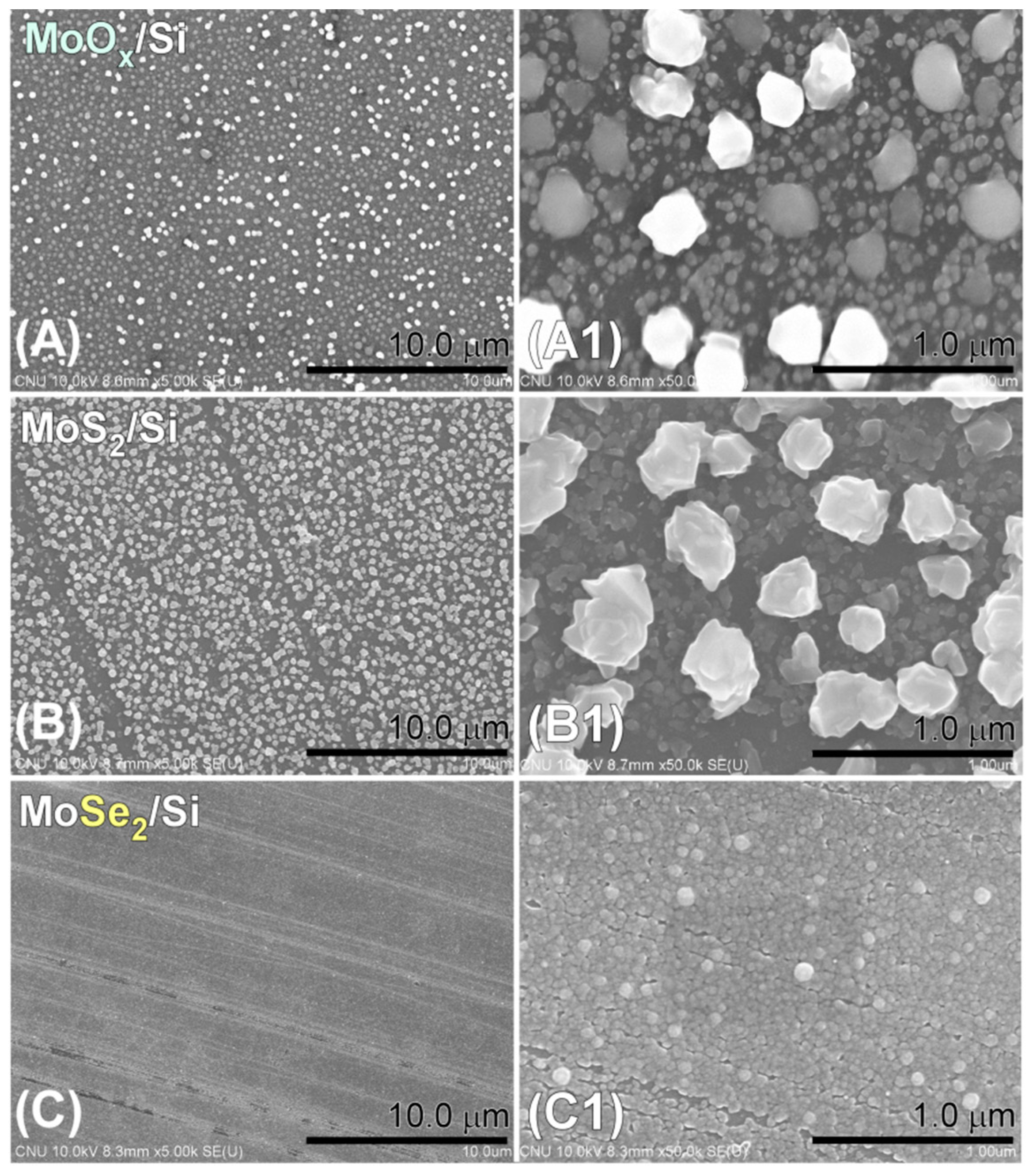
2.1. SEM Morphology
2.2. Raman Spectroscopy
2.3. X-ray Photoelectron Spectroscopy
2.4. Photoelectrochemcial Hydrogen Evolution
2.5. Photoelectrochemcial CO2 Reduction
3. Discussion
4. Materials and Methods
5. Conclusions
- Mo oxides were successfully electrodeposited on a Si support under visible light exposure. Under the dark condition, the electrochemical deposition was less efficient.
- A rapid-thermal annealing method was successfully introduced for the electrodeposited MoOx/Si to fabricate MoS2/Si and MoSe2/Si catalyst systems. Other impurity phases were not detected mainly based on the Raman and XPS results. The maximum temperature was achieved by rapid heating to 700 °C of S or Se powers on the MoOx/Si and maintained for 6 sec.
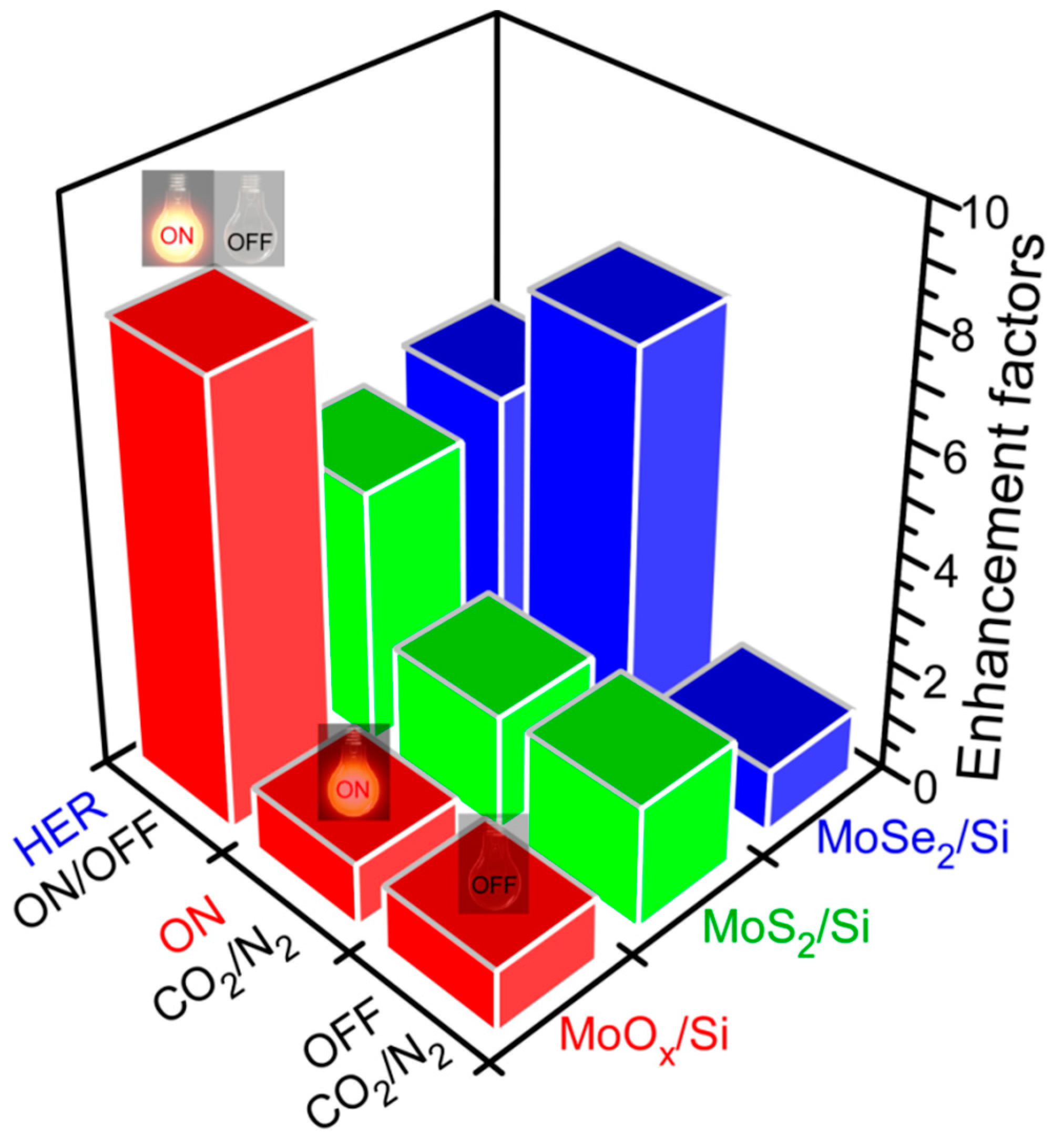
- HER tests in 0.1 M H2SO4 electrolyte showed a catalytic activity order of MoOx/Si < MoS2/Si << MoSe2/Si under dark and visible light-on conditions. The HER activity (4.5 mA/cm2 at −1.0 V vs Ag/AgCl) of MoSe2/Si was increased by 4.8× compared with that under the dark condition.
- CO2 reduction tests in 0.1 M NaHCO3 electrolyte showed a catalytic activity order of MoOx/Si, MoS2/Si << MoSe2/Si and MoS2/Si < MoOx/Si << MoSe2/Si under dark and visible light-on conditions, respectively. The reduction activity (0.127 mA/cm2) of MoSe2/Si was increased by 9.3× compared with that under the dark condition.
Author Contributions
Funding
Acknowledgments
Conflicts of Interest
References
- Yang, L.; Liu, P.; Li, J.; Xiang, B. Two-dimensional material molybdenum disulfides as electrocatalysts for hydrogen evolution. Catalysts 2017, 7, 285. [Google Scholar] [CrossRef]
- Theerthagiri, J.; Senthil, R.A.; Senthilkumar, B.; Polu, A.R.; Madhavan, J.; Ashokkumar, M. Recent advances in MoS2 nanostructured materials for energy and environmental applications—A review. J. Sol. Stat. Chem. 2017, 252, 43–71. [Google Scholar] [CrossRef]
- Eftekhari, A. Molybdenum diselenide (MoSe2) for energy storage, catalysis and optoelectronics. Appl. Mater. Today 2017, 8, 1–17. [Google Scholar] [CrossRef]
- Francis, S.A.; Velazquez, J.M.; Ferrer, I.M.; Torelli, D.A.; Guevarra, D.; McDowell, M.T.; Sun, K.; Zhou, X.; Saadi, F.H.; John, J.; et al. Reduction of aqueous CO2 to 1-propanol at MoS2 Electrodes. Chem. Mater. 2018, 30, 4902–4908. [Google Scholar] [CrossRef]
- Guo, W.; Chen, Y.; Wang, L.; Xu, J.; Zeng, D.; Peng, D.L. Colloidal synthesis of MoSe2 nanonetworks and nanoflowers with efficient electrocatalytic hydrogen-evolution activity. Electrochim. Acta 2017, 231, 69–76. [Google Scholar]
- Guo, H.; Jin, C.; Liu, X.; Liu, J.; Vasileff, A.; Jiao, Y.; Zheng, Y.; Qiao, S. Emerging Two-dimensional nanomaterials for electrocatalysis. Chem. Rev. 2018, 118, 6337–6408. [Google Scholar]
- Mao, J.; Wang, Y.; Zheng, Z.; Deng, D. The rise of two-dimensional MoS2 for catalysis. Front. Phys. 2018, 13, 138118. [Google Scholar] [CrossRef]
- Sun, Z.; Ma, T.; Tao, H.; Fan, Q.; Han, B. Fundamentals and challenges of electrochemical CO2 reduction using two-dimensional materials. Chem 2017, 3, 560–587. [Google Scholar] [CrossRef]
- Gupta, U.; Rao, C.N.R. Hydrogen generation by water splitting using MoS2 and other transition metal dichalcogenides. Nano Energy 2017, 41, 49–65. [Google Scholar] [CrossRef]
- Eftekhari, A. Electrocatalysts for hydrogen evolution reaction. Int. J. Hydrog. Eng. 2017, 42, 11053–11077. [Google Scholar] [CrossRef]
- Cai, Z.; Liu, B.; Zou, X.; Cheng, H. Chemical vapor deposition growth and applications of two-dimensional materials and their heterostructures. Chem. Rev. 2018, 118, 6091–6133. [Google Scholar] [CrossRef]
- Ye, G.; Gong, Y.; Lin, J.; Li, B.; He, Y.; Pantelides, S.T.; Zhou, W.; Vajtai, R.; Ajayan, P.M. Defects engineered monolayer MoS2 for improved hydrogen evolution reaction. Nano Lett. 2016, 16, 1097–1103. [Google Scholar] [CrossRef]
- Meng, C.; Lin, M.C.; Du, X.; Zhou, Y. Molybdenum disulfide modified by laser irradiation for catalyzing hydrogen evolution. ACS Sustain. Chem. Eng. 2019, 7, 6999–7003. [Google Scholar] [CrossRef]
- He, Z.; Zhao, R.; Chen, X.; Chen, H.; Zhu, Y.; Su, H.; Huang, S.; Xue, J.; Dai, J.; Cheng, S.; et al. Defect engineering in single-layer MoS2 using heavy ion irradiation. ACS Appl. Mater. Interfaces 2018, 10, 42524–42533. [Google Scholar] [CrossRef]
- Xia, B.; Wang, T.; Jiang, X.; Zhang, T.; Li, J.; Xiao, W.; Xi, P.; Gao, D.; Xue, D.; Ding, J. Ar2+ beam irradiation-induced multivancancies in MoSe2 nanosheet for enhanced electrochemical hydrogen evolution. ACS Energy Lett. 2018, 3, 2167–2172. [Google Scholar] [CrossRef]
- Zhang, P.; Xiang, H.; Tao, L.; Dong, H.; Zhou, Y.; Hu, T.S.; Chen, X.; Liu, S.; Wang, S.; Garaj, S. Chemically activated MoS2 for efficient hydrogen production. Nano Energy 2019, 57, 535–541. [Google Scholar] [CrossRef]
- Li, G.; Zhang, D.; Qiao, Q.; Yu, Y.; Peterson, D.; Zafar, A.; Kumar, R.; Curtarolo, S.; Hunte, F.; Shannon, S.; et al. All the catalytic active sites of MoS2 for hydrogen evolution. J. Am. Chem. Soc. 2016, 138, 16632–16638. [Google Scholar] [CrossRef]
- Chang, K.; Hai, X.; Pang, H.; Zhang, H.; Shi, L.; Liu, G.; Liu, H.; Zhao, G.; Li, M.; Ye, J. Targeted synthesis of 2H- and 1T-phase MoS2 monolayers for catalytic hydrogen evolution. Adv. Mater. 2016, 28, 10033–10041. [Google Scholar] [CrossRef]
- Zhang, J.; Wang, T.; Liu, P.; Liu, Y.; Ma, J.; Gao, D. Enhanced catalytic activities of metal-phase-assisted 1T@2H-MoSe2 nanosheets for hydrogen evolution. Electrochim. Acta 2016, 217, 181–186. [Google Scholar] [CrossRef]
- Wang, J.; Yan, M.; Zhao, K.; Liao, X.; Wang, P.; Pan, X.; Yang, W.; Mai, L. Field effect enhanced hydrogen evolution reaction of MoS2 nanosheets. Adv. Mater. 2016, 29, 1604464. [Google Scholar] [CrossRef]
- Guo, J.; Li, F.; Sun, Y.; Zhang, X.; Tang, L. Oxygen-incorporated MoS2 ultrathin nanosheets grown on graphene for efficient electrochemical hydrogen evolution. J. Power Sources 2015, 291, 195–200. [Google Scholar] [CrossRef]
- Zhu, C.; Xu, Q.; Liu, W.; Ren, Y. CO2-assisted fabrication of novel heterostructures of h-MoO3/1T-MoS2 for enhanced photoelectrocatalytic performance. Appl. Surf. Sci. 2017, 425, 56–62. [Google Scholar] [CrossRef]
- Chen, X.; Liu, G.; Zheng, W.; Feng, W.; Cao, W.; Hu, W.; Hu, P. Vertical 2D MoO2/MoSe2 core–shell nanosheet arrays as high performance electrocatalysts for hydrogen evolution reaction. Adv. Funct. Mater. 2016, 26, 8537–8544. [Google Scholar] [CrossRef]
- Hong, X.; Chan, K.; Tsai, C.; Nørskov, J.K. How doped MoS2 breaks transition-metal scaling relations for CO2 electrochemical reduction. ACS Catal. 2016, 6, 4428–4437. [Google Scholar] [CrossRef]
- Chan, K.; Tsai, C.; Hansen, H.A.; Nørskov, J.K. Molybdenum sulfides and selenides as possible electrocatalysts for CO2 reduction. ChemCatChem 2014, 6, 1899–1905. [Google Scholar] [CrossRef]
- Ji, Y.; Norskov, J.K.; Chan, K. Scaling relations on basal plane vacancies of transition metal dichalcogenides for CO2 reduction. J. Phys. Chem. C 2019, 123, 4256–4261. [Google Scholar] [CrossRef]
- Jia, P.; Guo, R.; Pan, W.; Huang, C.; Tang, J.; Liu, X.; Qin, H.; Xu, Q. The MoS2/TiO2 heterojunction composites with enhanced activity for CO2 photocatalytic reduction under visible light irradiation. Colloids Surf. A 2019, 570, 306–316. [Google Scholar] [CrossRef]
- Asadi, M.; Kumar, B.; Behranginia, A.; Rosen, B.A.; Baskin, A.; Repnin, N.; Pisasale, D.; Phillips, P.; Zhu, W.; Haasch, R.; et al. Robust carbon dioxide reduction on molybdenum disulphide edges. Nat. Commun. 2014, 5, 4470. [Google Scholar] [CrossRef] [Green Version]
- Asadi, M.; Kim, K.; Liu, C.; Addepalli, A.V.; Abbasi, P.; Yasaei, P.; Phillips, P.; Behranginia, A.; Cerrato, J.M.; Haasch, R.; et al. Nanostructured transition metal dichalcogenide electrocatalysts for CO2 reduction in ionic liquid. Science 2016, 353, 467–470. [Google Scholar] [CrossRef]
- Bicelli, L.P.; Bozzini, B.; Mele, C.; D’Urzo, L. A review of nanostructural aspects of metal electrodeposition. Int. J. Electrochem. Sci. 2008, 3, 356–408. [Google Scholar]
- Petrova, M.L.; Bojinov, M.; Gadjov, I.H. Electrodeposition of molybdenum oxides from weakly alkaline ammonia-molybdate electrolytes. Bulg. Chem. Commun. 2011, 43, 60–63. [Google Scholar]
- Li, R.; Hao, H.; Huang, T.; Yu, A. Electrodeposited Pd–MoOx catalysts with enhanced catalytic activity for formic acid electrooxidation. Electrochim. Acta 2012, 76, 292–299. [Google Scholar] [CrossRef]
- Inguanta, R.; Spanò, T.; Piazza, S.; Sunseri, C.; Barreca, F.; Fazio, E.; Neri, F.; Silipigni, L. Electrodeposition and characterization of Mo oxide nanostructures. Chem. Eng. Trans. 2015, 43, 685–690. [Google Scholar]
- Banica, R.; Barvinschi, P.; Vaszilcsin, N.; Nyari, T. A comparative study of the electrochemical deposition of molybdenum oxides thin films on copper and platinum. J. Alloys Compd. 2009, 483, 402–405. [Google Scholar] [CrossRef]
- Soundeswaran, S.; Kumar, O.S.; Babu, S.M.; Ramasamy, P.; Dhanasekaran, R. Influence of ultrasonification in CdS thin film deposition in PCD technique. Mater. Lett. 2005, 59, 1795–1800. [Google Scholar] [CrossRef]
- Podder, J.; Kobayashi, R.; Ichimura, M. Photochemical deposition of CuxS thin films from aqueous solutions. Thin Solid Films 2005, 472, 71–75. [Google Scholar] [CrossRef]
- Zhang, W.L.; Zhang, S.; Yang, M.; Chen, T.P. Microstructure of magnetron sputtered amorphous SiOx films: Formation of amorphous Si core-shell nanoclusters. J. Phys. Chem. C 2010, 114, 2414–2420. [Google Scholar] [CrossRef]
- Wu, S.; Huang, H.; Shang, M.; Du, C.; Wu, Y.; Song, W. High visible light sensitive MoS2 ultrathin nanosheets for photoelectrochemical biosensing. Biosens. Bioelectron. 2017, 92, 646–653. [Google Scholar] [CrossRef]
- Deng, S.; Zhong, Y.; Zeng, Y.; Wang, Y.; Yao, Z.; Yang, F.; Lin, S.; Wang, X.; Lu, X.; Xia, X.; et al. Directional construction of vertical nitrogen-doped 1T-2H MoSe2/graphene shell/core nanoflake arrays for efficient hydrogen evolution reaction. Adv. Mater. 2017, 29, 1700748. [Google Scholar] [CrossRef]
- Jiang, Q.; Lu, Y.; Huang, Z.; Hu, J. Facile solvent-thermal synthesis of ultrathin MoSe2 nanosheets for hydrogen evolution and organic dyes adsorption. Appl. Surf. Sci. 2017, 402, 277–285. [Google Scholar] [CrossRef]
- Nam, D.; Lee, J.U.; Cheong, H. Excitation energy dependent Raman spectrum of MoSe2. Sci. Rep. 2015, 5, 17113. [Google Scholar] [CrossRef]
- Gu, J.I.; Lee, J.; Rhee, C.K.; Sohn, Y. Enhanced electrochemical hydrogen evolution over defect-induced hybrid MoO3/Mo3O9·H2O microrods. Appl. Surf. Sci. 2019, 469, 348–356. [Google Scholar] [CrossRef]
- Xu, X.B.; Sun, Y.; Qiao, W.; Zhang, X.; Chen, X.; Song, X.Y.; Du, Y.W. 3D MoS2-graphene hybrid aerogels as catalyst for enhanced efficient hydrogen evolution. Appl. Surf. Sci. 2017, 396, 1520–1527. [Google Scholar] [CrossRef]
- Jian, W.; Cheng, X.; Huang, Y.; You, Y.; Zhou, R.; Sun, T.; Xu, J. Arrays of ZnO/MoS2 nanocables and MoS2 nanotubes with phase engineering for bifunctional photoelectrochemical and electrochemical water splitting. Chem. Eng. J. 2017, 328, 474–483. [Google Scholar] [CrossRef]
- Zhang, J.; Wu, M.H.; Shi, Z.T.; Jiang, M.; Jian, W.J.; Xiao, Z.; Li, J.; Lee, C.S.; Xu, J. Composition and interface engineering of alloyed MoS2xSe2(1–x) nanotubes for enhanced hydrogen evolution reaction activity. Small 2016, 12, 4379–4385. [Google Scholar] [CrossRef]
- Upadhyay, K.K.; Nguyen, T.; Silva, T.M.; Carmezim, M.J.; Montemor, M.F. Electrodeposited MoOx films as negative electrode materials for redox supercapacitors. Electrochim. Acta 2017, 225, 19–28. [Google Scholar] [CrossRef]
- Liu, C.; Xie, Z.; Wang, W.; Li, Z.; Zhang, Z. Fabrication of MoOx film as a conductive anode material for micro-supercapacitors by electrodeposition and annealing. J. Electrochem. Soc. 2014, 161, A1051–A1057. [Google Scholar] [CrossRef]
- Guo, L.; Oskam, G.; Radisic, A.; Hoffmann, P.M.; Searson, P.C. Island growth in electrodeposition. J. Phys. D 2011, 44, 443001. [Google Scholar] [CrossRef]
- Shu, H.; Zhou, D.; Li, F.; Cao, D.; Chen, X. Defect engineering in MoSe2 for the hydrogen evolution reaction: From point defects to edges. ACS Appl. Mater. Interfaces 2017, 9, 42688–42698. [Google Scholar] [CrossRef]
- Ravikumar, C.H.; Nair, G.V.; Muralikrishna, S.; Nagaraju, D.H.; Balakrishna, R.G. Nanoflower like structures of MoSe2 and MoS2 as efficient catalysts for hydrogen evolution. Mater. Lett. 2018, 220, 133–135. [Google Scholar] [CrossRef]
- Sekizawa, K.; Oh-Ishi, K.; Kataoka, K.; Arai, T.; Suzuki, T.M.; Morikawa, T. Stoichiometric water splitting using p-type Fe2O3 based photocathode with the aid of multi-heterojunction. J. Mater. Chem. A 2017, 5, 6483–6493. [Google Scholar] [CrossRef]
- Briggs, D.; Seah, M.P. Practical Surface Analysis, 2nd ed.; Wiley and Sons: Hoboken, NJ, USA, 1990; Volume 1. [Google Scholar]
- Tosini, G.; Ferguson, I.; Tsubota, K. Effects of blue light on the circadian system and eye physiology. Mol. Vis. 2016, 22, 61–72. [Google Scholar] [PubMed]


© 2019 by the authors. Licensee MDPI, Basel, Switzerland. This article is an open access article distributed under the terms and conditions of the Creative Commons Attribution (CC BY) license (http://creativecommons.org/licenses/by/4.0/).
Share and Cite
Hong, S.; Rhee, C.K.; Sohn, Y. Photoelectrochemical Hydrogen Evolution and CO2 Reduction over MoS2/Si and MoSe2/Si Nanostructures by Combined Photoelectrochemical Deposition and Rapid-Thermal Annealing Process. Catalysts 2019, 9, 494. https://doi.org/10.3390/catal9060494
Hong S, Rhee CK, Sohn Y. Photoelectrochemical Hydrogen Evolution and CO2 Reduction over MoS2/Si and MoSe2/Si Nanostructures by Combined Photoelectrochemical Deposition and Rapid-Thermal Annealing Process. Catalysts. 2019; 9(6):494. https://doi.org/10.3390/catal9060494
Chicago/Turabian StyleHong, Sungmin, Choong Kyun Rhee, and Youngku Sohn. 2019. "Photoelectrochemical Hydrogen Evolution and CO2 Reduction over MoS2/Si and MoSe2/Si Nanostructures by Combined Photoelectrochemical Deposition and Rapid-Thermal Annealing Process" Catalysts 9, no. 6: 494. https://doi.org/10.3390/catal9060494