Phase and Texture of Solution-Processed Copper Phthalocyanine Thin Films Investigated by Two-Dimensional Grazing Incidence X-Ray Diffraction


Abstract
: The phase and texture of a newly developed solution-processed copper phthalocyanine (CuPc) thin film have been investigated by two-dimensional grazing incidence X-ray diffraction. The results show that it has β phase crystalline structure, with crystallinity greater than 80%. The average size of the crystallites is found to be about 24 nm. There are two different arrangements of crystallites, with one dominating the diffraction pattern. Both of them have preferred orientation along the thin film normal. Based on the similarities to the vacuum deposited CuPc thin films, the new solution processing method is verified to offer a good alternative to vacuum process, for the fabrication of low cost small molecule based organic photovoltaics.1. Introduction
Small molecule based organic photovoltaics (OPVs) have better stabilities than polymer based OPVs due to their intrinsic thermal and chemical properties [1,2]. However, small molecule based OPVs are usually prepared by a more costly vacuum deposition process, as opposed to solution process for polymer based OPVs [3,4]. It is therefore desirable to make low cost small molecule based OPVs by solution processing. Due to the limited solubility, surfactants are usually necessary to dissolve small organic molecules, which would decrease the conductivity, resulting from the presence of surfactants blocking the electron/hole transport [5], thus affecting negatively the performance of small molecule based OPVs.
To resolve the problem, a new method has recently been proposed in our group, to fabricate small molecule based thin films without surfactants, via precipitation and spray-coating of a concentrated copper phthalocyanine (CuPc) acid mixture [6]. In order to achieve the same level of performance, it is necessary to confirm, before the device fabrication, that the new films have similar structure and morphology to that of vacuum deposited thin films. Prepared by a careful control of deposition parameters, the vacuum deposited films are usually highly crystalline, with uni-axial orientation along the surface normal [7-9]. The application of X-ray diffraction (XRD) analysis is necessary to fully characterize the crystallite phase and orientation information, which is crucial in device fabrication [10]. To accomplish this goal, grazing incidence X-ray diffraction (GIXRD) has been used, since it offers more direct information than, e.g., selected area electron diffraction performed by transmission electron microscopy [11], where the crystal structure and orientation cannot be obtained without the substrate removal. In addition, a two-dimensional (2-D) area detector has been employed here, to obtain more complete crystal information than the diffraction intensity versus 2θ plot [12] where crystallite orientation cannot be obtained as efficiently.
It is therefore the purpose of this report to present crystal phase and orientation studies of our newly developed solution processed CuPc thin film. Various phases can be obtained depending on different processing parameters [13]. In our solution processed β-phase CuPc thin film, two different crystallite fiber orientations ([201̄] and [001] normal to surface) were found to co-exist, with (201̄) orientation dominating the diffraction pattern. Compared to the vacuum deposited α-phase CuPc thin films with (100) and (110) fiber orientations [9], our new crystalline thin films have similar crystallite sizes [3,7]. The similarities clearly show that the new solution processing method offers an excellent alternative to vacuum process, for the fabrication of low cost small molecule based OPVs.
2. Results and Discussion
2.1. Crystal Structure of Solution-processed CuPc Thin Film
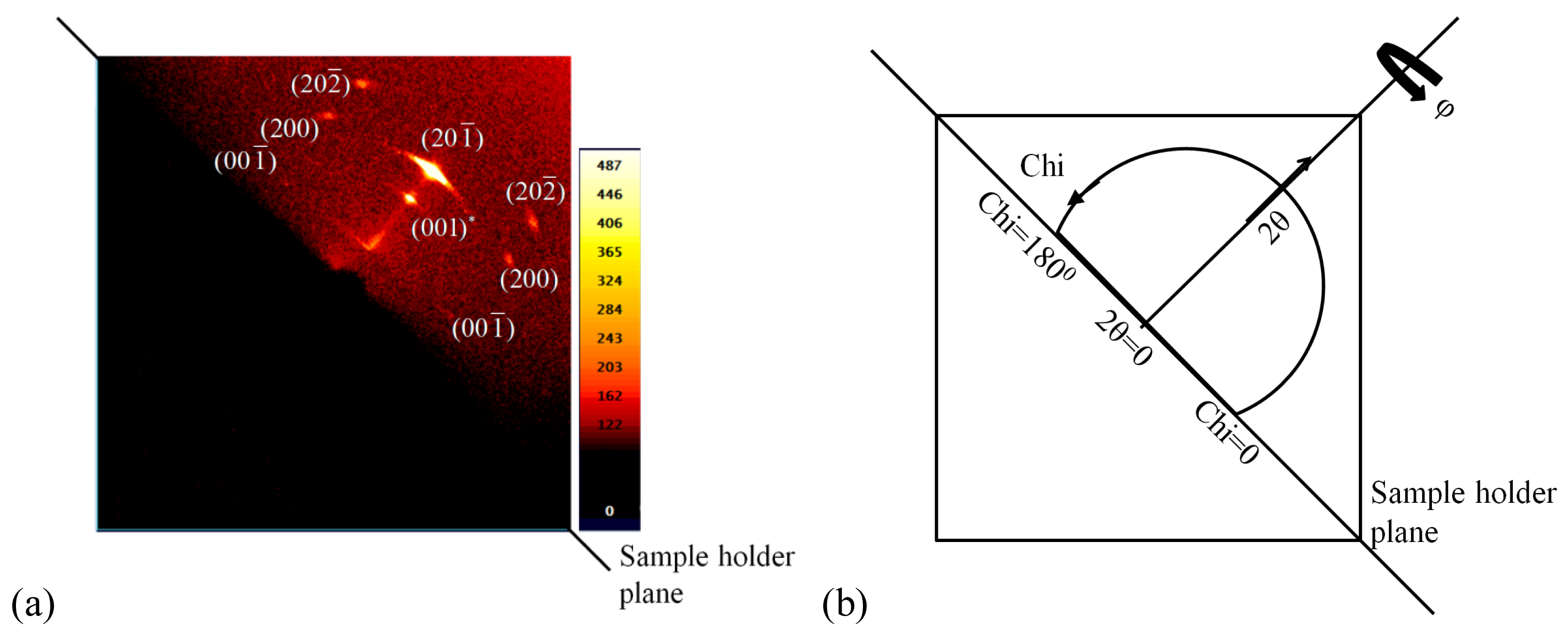
Figure 1a shows the two-dimensional (2-D) diffraction pattern of the thin film obtained by grazing incident X-ray (incident X-ray angle at 2°), performed on the newly developed solution-processed CuPc thin film (thickness: ∼100 nm) on top of an indium tin oxide (ITO) conducting glass substrate (ITO thickness: ∼50 nm; glass thickness: ∼1 mm). The diagonal from the top left to the bottom right shows the side view of sample holder (Figure 1a). The frame shows strong diffraction spots from four sets of lattice planes, with 2θ peak width varying between 0.4° and 1.1°. The chi spread of (001) is 18.7°, and 28.8° for (201̄), obtained by GADDS software [14], Very weak (001̄) signals can be observed in Figure 1a near the plane of the thin film. The crystallinity of the thin film is found to be greater than 80%, calculated again by GADDS software [14].
While these diffraction features are produced by the reciprocal lattice points intercepting the Ewald sphere, they do not necessarily represent a single crystal, due to the arbitrary choice of φ angle. Because the typical diffraction pattern does not vary with φ (Figure 1b), the spots in Figure 1a actually represent polycrystalline fiber-type arrangements, with a preferred orientation along the thin film normal (from the center to the upper–right), and random crystallite orientation in the plane of the film.
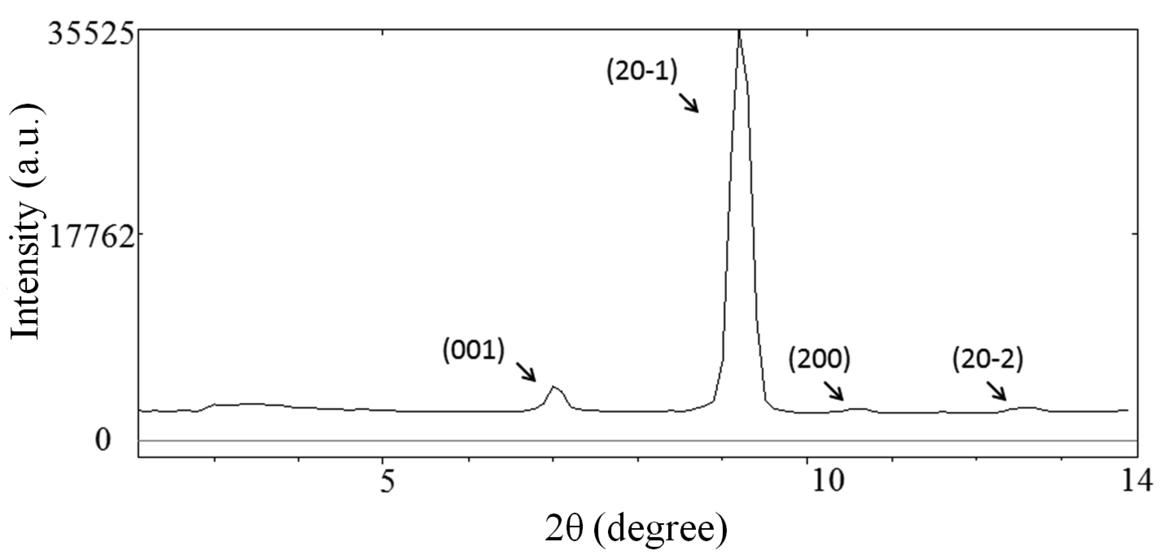
To analyze the phase composition, the diffraction intensity versus 2θ plot (Figure 2) was obtained by integrating Chi from 0 to 180° from Figure 1a and 1b, using GADDS software [14] and PowderCell software [15]. Our solution-processed CuPc has been determined to be the β phase. The lattice parameters are as follows: a = 19.407 Å, b = 4.7900 Å, c= 14.628 Å; β = 120.560° ± 0.003°, α = γ = 90°; non-standard space group: P21/a, Z = 2 [13,16]. The four peaks (Figure 2) represent the (001), (201̄), (200) and (20 2̄) lattice planes, located at 2θ of 7.03°, 9.21°, 10.59° and 12.54°, respectively. Compared to the α-CuPc thin film usually obtained by vacuum deposition, the β-CuPc phase we obtained by the solution process is a more thermodynamically stable structure, which is usually formed above 210 °C or under the influence of organic solvents [13]. The average crystallite size is found to be about 24 nm, calculated from the full width at half-maximum (FWHM = 0.35°) of the peak at 2θ of 9.21°, using the Debye-Scherrer formula [17]. This is correlated to Kewei Wang et al.'s results obtained from scanning electron microscopy (SEM) [6]. It is similar to that of the vacuum deposited α-CuPc thin films, which have crystallite sizes between 10 and 50 nm, depending on the substrate temperatures [3,7,9,18].
2.2. Preferred Orientation of the Crystallites
As described above, the thin film had strong textures (highly preferred orientations of crystallites), as shown by the limited Chi intensity distribution.
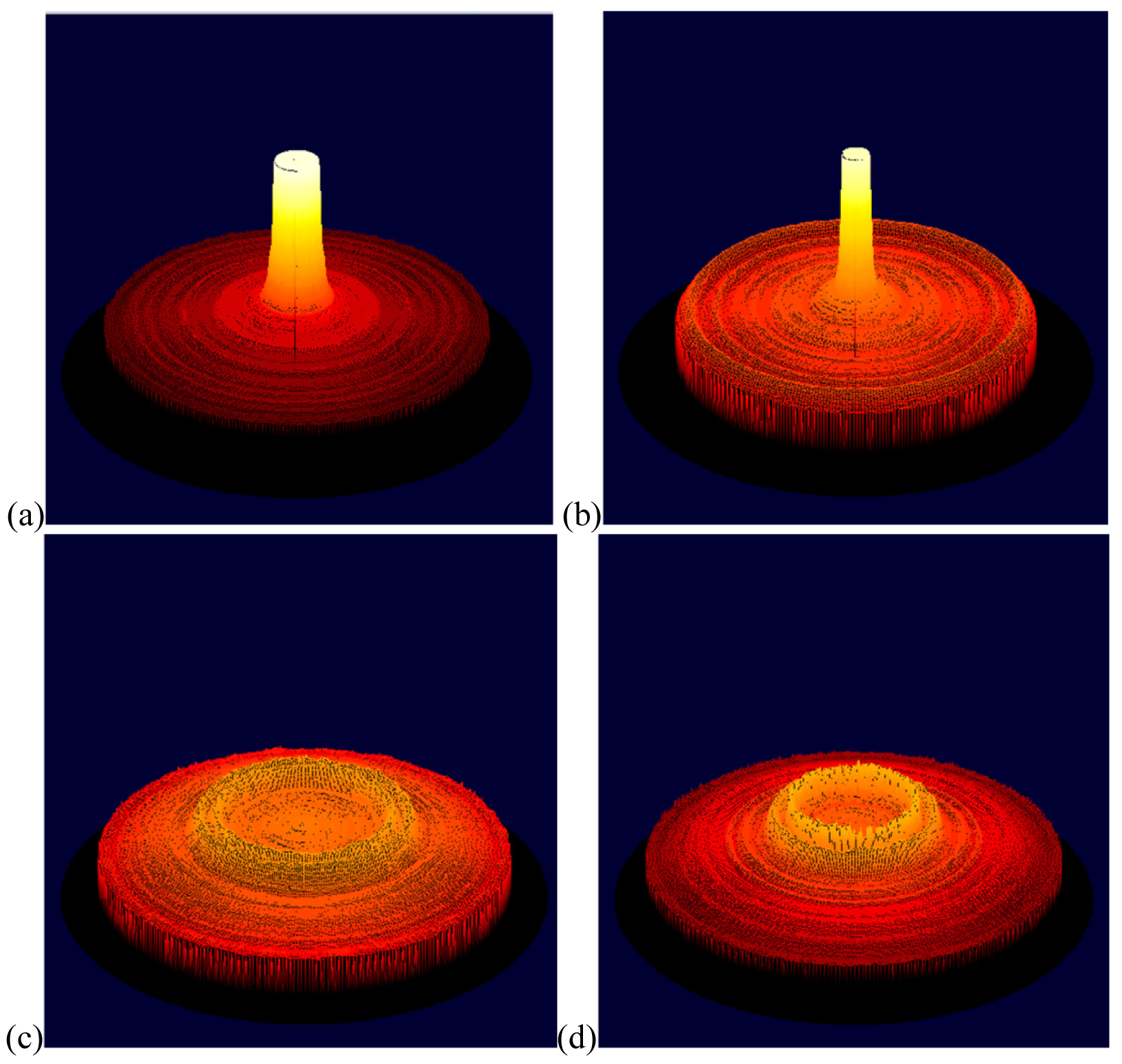
To analyze the preferred orientation, the intensity distribution of each lattice plane with respect to the sample coordinates in stereographic projection was plotted (using GADDS software [14], assuming fiber geometry), as a pole figure. As shown by the three-dimensional (3-D) surface plot of the (201̄) pole figure (Figure 3a), enhanced pole intensity (marked with brighter color) is located exactly in the center of the figure. It reveals that the β-CuPc crystallites were oriented with the (201̄) planes parallel to the substrate. In addition, the 3-D surface plot of (001) pole figure (Figure 3b) demonstrates that the (001) planes were parallel to the substrate.
However, within a single crystallite, (001) planes cannot be parallel to (201̄) planes, as they form an angle of 99.656°. Therefore, there must be two different fiber textures coexisting in our thin film. A possible reason for the two types of fiber textures observed is that the arrangement of CuPc crystallites is more stable along (001) and (201̄) directions. The indium tin oxide (ITO) substrate does not affect the fiber textures, since the ITO glass did not receive any further pretreatment except for cleaning, and the ITO glass itself is polycrystalline with no preferred orientation.
Moreover, the four diffraction features in Figure 1a, resulting from (200) and (202̄) planes, correlate with the (201̄) fiber orientation (Figure 3c and d), and represent the intersection of rings of diffraction with the 2-D detector [19], The weak (001̄) signal near the plane of the thin film in Figure 1a comes from (201̄) fiber orientation as well. As a result, (201̄)-normal orientation dominates the diffraction pattern in Figure 1a. Only a small fraction of crystallites were found to be in the (001)-normal orientation, thus the (200) and (202̄) diffraction intensities were too low to be observed from the crystallites in (001) orientation.
Therefore, it is found that β-CuPc crystallites, in the newly developed thin film, have two preferred orientations with one dominating. A similar situation exists in the vacuum deposited thin film, where the (100) and (110) orientations of the α-phase are the commonly preferred axial orientations [9].
2.3. The Arrangement of CuPc Crystallites in the Thin Film
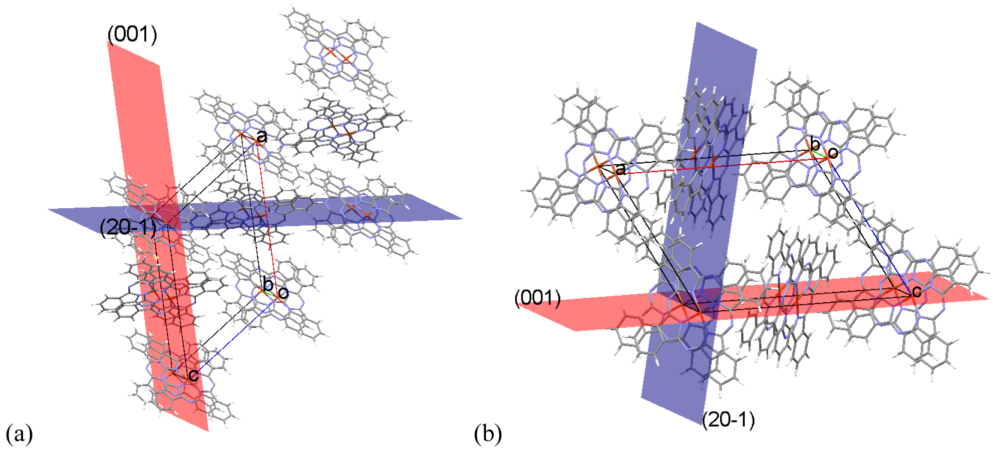
From the discussion above, it becomes evident that two different types of preferred orientations can be found in the newly developed solution-processed CuPc thin film .The (201̄) and (001) orientations of the crystallites are characterized by the (201̄) and (001) lattice planes parallel to the substrate. Therefore, the molecular arrangements of β-CuPc can be depicted, as shown by Figure 4. CuPc molecules aggregate as tilted stacks (along [010]), with an almost rectangular cross-section. A majority of crystallites are arranged in the (201̄) orientation as described by Figure 4a. A minority of crystallites are arranged in the (001) orientation, as illustrated by Figure 4b. The packing of the molecular stacks on their (201̄) surface allows the molecules to lie at a shallower angle to the surface. The only other packing option is for the stacks to rotate approximately 90 degrees on axis and lie on the (001) surface. In this less populated orientation the molecules are at a much higher inclination to the surface.
3. Experimental Section
As for the strategy we used to prepare CuPc thin films, we firstly precipitated CuPc-H2SO4 mixture into water to obtain the surfactant-free CuPc nanoparticles. Then, the CuPc nanoparticles were washed by water, dried in a vacuum oven at 70 °C, and were deposited on the substrate by spray coating [6]. Two-dimensional grazing-incidence X-ray diffraction was employed to measure the thin film texture [19]. The orientation distribution of several crystallographic planes over a range of angles was measured simultaneously; in addition the textures were observed directly from the 2-D diffraction frame. Figure 5 shows a schematic illustration of the two-dimensional grazing-incidence X-ray diffraction measurement employed in our experiment.
The distance between the 2-D detector and the sample mount was 16.715 cm (Figure 5). The experiment was performed at room temperature on a Bruker Smart 6000 CCD 3-circle D8 diffractometer with a Cu RA (Rigaku Ru200) parallel focused X-ray source (λ = 1.5418 Å). The data were collected at still mode with 300 seconds per frame and processed with GADDS software [14].
Since the 2D diffraction image of our CuPc thin film shows a distribution of orientation, in GADDS software, “External Method” is used for a relative measurement of crystallinity. By determining the boundaries of the amorphous region and crystalline region, with the same 2θ limits and different chi range, the GADDS software can calculate the crystallinity by employing specified areas of frame data [14]. The calculating result shows that the crystallinity of our CuPc thin film is greater than 80%.
4. Conclusion
To summarize, the crystalline phase and orientation information has been analyzed for our newly developed solution-processed CuPc thin films by 2-D grazing incidence X-ray diffraction. The results show that the film has a crystallinity greater than 80%, and an average crystallite size about 24 nm, similar to that of the vacuum deposited thin films. In addition, crystallites in the thin film had two preferred orientations (201̄) and (001), with (201̄) dominating. The crystallites in both orientations have a preferential ordering along the substrate normal, and are randomly oriented in-plane. Thus, our new method to prepare CuPc thin film offers an excellent alternative to the vacuum deposited films, for the manufacture of low cost small molecule based OPVs in the future.


Acknowledgments
The authors want to acknowledge the support from National Science and Engineering Research Council of Canada.
References
- Xue, J.; Rand, B.P.; Uchida, S.; Forrest, S.R. A hybrid planar-mixed molecular heterojunction photovoltaic cell. Adv. Mater. 2005, 17, 66–71. [Google Scholar]
- Perez, M.D.; Borek, C.; Forrest, S.R.; Thompson, M.E. Molecular and morphological influences on the open circuit voltages of organic photovoltaic devices. J. Am. Chem. Soc. 2009, 131, 9281–9286. [Google Scholar]
- Peumans, P.; Uchida, S.; Forrest, S.R. Efficient bulk heterojunction photovoltaic cells using small- molecular-weight organic thin films. Nature 2003, 425, 158–162. [Google Scholar]
- Steinberger, S.; Mishra, A.; Reinold, E.; Levichkov, J.; Uhrich, C.; Pfeiffer, M; Bäuerle, P. Vacuum-processed small molecule solar cells based on terminal acceptor-substituted low-band gap oligothiophenes. Chem. Commun. 2011, 47, 1982–1984. [Google Scholar]
- Verma, D.; Rao, A.R.; Dutta, V. Surfactant-free CdTe nanoparticles mixed MEH-PPV hybrid solar cell deposited by spin coating technique. Solar Energ. Mater. Solar Cells 2009, 93, 1482–1487. [Google Scholar]
- Wang, K.W. McMaster University: Hamilton, ON, Canada; Personal Communication; 2011. [Google Scholar]
- Rusu, M.; Gasiorowski, J.; Wiesner, S.; Meyer, N.; Heuken, M.; Fostiropoulos, K.; Lux-Steiner, M.C. Fine tailored interpenetrating donor-acceptor morphology by OVPD for organic solar cells. Thin Solid Films 2008, 516, 7160–7166. [Google Scholar]
- Ofuji, M.; Inaba, K.; Omote, K.; Hoshi, H.; Takanishi, Y; Ishikawa, K.; Takezoe, H. Grazing incidence in-plane X-ray diffraction study on oriented copper phthalocyanine thin films. Jpn. J. appl. Phys. 2001, 41, 5467–5471. [Google Scholar]
- Resel, R.; Ottmar, M.; Hanack, M.; Keckes, J.; Leising, G. Preferred orientation of copper phthalocyanine thin films evaporated on amorphous substrates. J. Mater. Res. 2000, 15, 934–939. [Google Scholar]
- Varotto, A.; Nam, C.; Radovpjevic, I.; Tomé, J.P.C.; Cavaleiro, J.A.S.; Black, C.T.; Drain, C.M. Phthalocyanine blends improve bulk heterojunction solar cells. J. Am. Chem. Soc. 2010, 132, 2522–2554. [Google Scholar]
- Sánchez-Díaz, A.; Pacios, R.; Munecas, U.; Torres, T.; Palomares, E. Charge transfer reactions in near IR absorbing small molecule solution processed organic bulk-heterojunction solar. Org. Electron. 2011, 12, 329–335. [Google Scholar]
- Schumann, S.; Hatton, R.A.; Jones, T.S. Organic photovoltaic devices based on water-soluble copper phthalocyanine. J. Phys. Chem. C 2011, 115, 4916–4921. [Google Scholar]
- Hiesgen, R.; Räbisch, M.; Böttcher, H.; Meissner, D. STM investigation of the growth structure of Cu-phthalocyanine films with submolecular resolution. Solar Energ. Mater. Solar Cells 2000, 61, 73–85. [Google Scholar]
- GADDS: General Area Detector Diffraction System, V4.1.29; Bruker Analytical X-ray Systems Inc.: Madison, WI, USA, 1999.
- PowderCell, V2.4; Federal Institute for Materials Research and Testing: Berlin, Germany, 2000.
- Orsa, A. 11-0893, β-copper Phthalocyanine; International Center for Diffraction Data: Newtown Square, PA, USA. Available online: www.icdd.com, PCPDFWIN Software V 2.4, 2003 (accessed on 10 March 2011).
- Hall, B.D.; Zanchet, D.; Ugarte, D. Estimating nanoparticle size from diffraction measurements. J. Appl. Cryst. 2000, 33, 1335–1341. [Google Scholar]
- Hsiao, Y.S.; Whang, W.T.; Suen, S.C. Morphological control of CuPc and its application in organic solar cells. Nanotechnology 2008, 19, 415603–415610. [Google Scholar]
- He, B. Two-Dimensional X-Ray Diffractions, 1st ed.; John Wiley & Sons, Inc.: Hoboken, NJ, USA, 2009; pp. 218–219. [Google Scholar]
- Mercury, V2.4; The Cambridge Crystallographic Data Centre: Cambridge, UK, 2011.
© 2011 by the authors; licensee MDPI, Basel, Switzerland. This article is an open access article distributed under the terms and conditions of the Creative Commons Attribution license (http://creativecommons.org/licenses/by/3.0/).
Share and Cite
Deng, L.; Wang, K.; Zhao, C.X.; Yan, H.; Britten, J.F.; Xu, G. Phase and Texture of Solution-Processed Copper Phthalocyanine Thin Films Investigated by Two-Dimensional Grazing Incidence X-Ray Diffraction. Crystals 2011, 1, 112-119. https://doi.org/10.3390/cryst1030112
Deng L, Wang K, Zhao CX, Yan H, Britten JF, Xu G. Phase and Texture of Solution-Processed Copper Phthalocyanine Thin Films Investigated by Two-Dimensional Grazing Incidence X-Ray Diffraction. Crystals. 2011; 1(3):112-119. https://doi.org/10.3390/cryst1030112
Chicago/Turabian StyleDeng, Lulu, Kewei Wang, Cindy X. Zhao, Han Yan, James F. Britten, and Gu Xu. 2011. "Phase and Texture of Solution-Processed Copper Phthalocyanine Thin Films Investigated by Two-Dimensional Grazing Incidence X-Ray Diffraction" Crystals 1, no. 3: 112-119. https://doi.org/10.3390/cryst1030112
APA StyleDeng, L., Wang, K., Zhao, C. X., Yan, H., Britten, J. F., & Xu, G. (2011). Phase and Texture of Solution-Processed Copper Phthalocyanine Thin Films Investigated by Two-Dimensional Grazing Incidence X-Ray Diffraction. Crystals, 1(3), 112-119. https://doi.org/10.3390/cryst1030112