
Termination Control of (001) and (110) NdGaO3 Single-Crystal Substrates by Selective Chemical Etching
Extreme Light Infrastructure-Nuclear Physics, “Horia Hulubei” National Institute for R&D in Physics and Nuclear Engineering, 30 Reactorului Street, 077125 Magurele, Romania
Crystals 2022, 12(12), 1791; https://doi.org/10.3390/cryst12121791
Submission received: 4 November 2022
/
Revised: 3 December 2022
/
Accepted: 7 December 2022
/
Published: 9 December 2022
(This article belongs to the Special Issue Ferroelectric Materials)
Abstract
:Controlling the surface morphology and composition of the perovskite substrates is a critical aspect in tuning the final properties of the deposited films and of their interfaces. The paper reports on a chemical etching method developed for (110) and (001) NdGaO3 single crystal substrates in order to obtain a well-defined GaO2−x-terminated surface. The etching process is based on a HF + NH4OH solution and includes an annealing step performed in air or under O2 flow at temperatures of 800–1000 °C. In order to obtain the desired composition and surface morphology, the etching procedure was optimized for the vicinal step density at the surface and substrate crystal orientation. Growth nucleation studies of one-unit-cell MeO films (Me = Ti, Sr, Ba) on chemically etched and on only annealed substrates were performed in order to determine the composition of the substrate topmost layer. The results indicate that the chemically etched NdGaO3 substrate surface has a predominantly GaO2−x termination, with a lower free surface energy compared to the NdO1+x termination.
1. Introduction
When growing films of compounds featuring a layered (perovskite) structure, the composition of the substrate-terminating atomic layer determines the surface morphology of the film [1], as well as the atomic stacking sequence of the substrate–film interface [2]. Consequently, this influences the final physico-chemical properties of the films [3,4,5,6,7]. It is, therefore, desirable for the lattice mismatch between the substrate and the film to be as small as possible in order to obtain a coherent crystalline growth [7,8]. Furthermore, studies of the novel properties arising at the interface between complex oxides, such as orbital reconstruction [9] or electronic coupling [10], require the fabrication of thin-film heterostructures with an atomic-scale roughness of the individual components. Therefore, precise atomic control of the interfaces in such multilayer structures depends on using substrates with known composition of their terminating layers. Surface treatments adapted to the substrate’s surface chemistry and their miscut angle are therefore required in order to produce atomically smooth, single-terminated substrate surfaces for ensuring reproducible thin-film growth.
NdGaO3 single crystals, in either (001) or (110) orientation, represent the only oxide material among the lanthanide gallates with no structural phase transitions below ~1000 °C. NdGaO3 is therefore often used to grow twin-free thin films when their deposition is performed at temperatures lower than its phase transition temperature [7,11,12,13,14,15,16]. As a perovskite substrate, NdGaO3 is intensively used for deposition of ferroelectric films and superlattices with excellent structural and electrical characteristics [17,18,19], allowing ferroelectric properties, such as the Curie point, to be tuned by the epitaxial strain [17,20,21].
Long-range ordering of ferroelectric stripe nano−domains was observed in (110)-oriented BiFeO3 thin films epitaxially grown on low-symmetric (110) NdGaO3 substrates [22]. Strained ferroelectric thin films epitaxially grown on appropriate substrates can exhibit properties that are superior to their bulk counterparts [20]. Properties of engineered ferroelectric materials, such as electro-strictive effect [23,24] and tunable ferroelectricity in artificial heterostructures [25], requires atomically controlled film–substrate interfaces.
Single-crystal X-ray [26,27,28], neutron [29], or synchrotron diffraction data [30] showed that, at room temperature, NdGaO3 features a layered GdFeO3 type structure (distorted perovskite with an orthorhombic symmetry, space group Pbnm) [30]. This polar perovskite consists of alternating stacks in the (001) direction of charged NdO+ and GaO2- atomic layers [31], with NdO1+x being a base character oxide, whereas GaO2−x is an amphoteric oxide (x stands for oxygen of unknown stoichiometry that takes into account charge neutrality) [29,30,31,32]. When the crystal is cut along the (110) plane, the resulting pseudo-cubic (pc) cell, which is slightly distorted in comparison with the primitive perovskite structure according to neutron powder diffraction studies [29], will have apc = bpc = 0.5(ao2 + bo2)1/2 = 3.863 Å, cpc = co/2 = 3.854 Å, γ = 89.26°, where ao, bo, and co represent the cell parameters of the orthorhombic unit cell, while γ corresponds to the angle between the apc and bpc axes, which deviates from 90° [29,33]. A selection of structural and physical properties of NdGaO3 is given in Table 1 [7].
The surface of the commercially available (as-received) substrates is characterized by a mixed termination of NdO1+x and GaO2−x, with structural defects and impurities due to mechanical polishing [34]. Low-temperature annealing, mostly performed at 500–600 °C under O2 flow (ex situ) or in vacuum, is generally used for the removal of surface contaminants. However, while the surface morphology is improved as a result of such thermal treatments, the mixed character of the termination layer remains [35] and the step ledges are rather imperfect, as shown in the AFM visualization of the surface morphology of an as-received (110) NdGaO3 substrate following low-temperature annealing (see Figure 1a). The streaky RHEED pattern (recorded at 550 °C and 5 × 10⁻² mbar O2) of the substrate indicates a disordered surface (see Figure 1b).
There are only a few studies on methods to control the surface morphology of the NdGaO3 substrates. In the case of (001)-oriented crystals, Ohnishi et al. [36] have shown that a NdO1+x single-terminated surface can be obtained by annealing in air for 2 h at high temperatures (1000 °C), with the composition of the terminating layer being analyzed thereafter using coaxial impact–collision ion scattering spectroscopy. A similar result (a single terminated surface) has been reported for (110) and (001) NdGaO3 substrates annealed in oxygen at temperatures of 800–950 °C, but the composition of the termination layer was not studied [37,38]. Auger electron spectroscopy [39] and low-energy ion scattering [40] measurements on (110) NdGaO3 substrates annealed at high temperatures (1000–1200 °C) under different gas fluxes (pure oxygen, argon, nitrogen, and air) indicate also a Nd-rich termination. However, the results of the annealing strongly depend on the substrate crystal orientation, the miscut angle (α) and its surface direction to the crystallographic axes (defined here as angle Δ), as well as on the atmosphere under which the annealing is performed (vacuum, air, or O2) [36,37,38,41,42,43,44]. Mixed terminated surfaces are typically observed if these parameters are not taken into account prior to carrying out the thermal treatments [41,44,45], as shown in Figure 1c for a (110) NdGaO3 substrate (miscut angle < 0.05°) annealed in air for 1 h, at 1000 °C. A clear mixed termination can be observed, as indicated by the formation of two types of terrace edges (round and saw-tooth-like). Another reason for the difficulty in controlling the surface morphology of the annealed samples may also arise from the presence of polishing or post-polishing contamination on the surface [34,35]. These impurities can be retained on the substrate surface even after subjecting it to heat treatment at temperatures as high as 1100 °C, as shown for SrTiO3 [46], therefore playing a crucial role in the evolution of the surface morphology.
The best method for not only removing the surface contaminants, but also for controlling the chemistry of the substrate termination layer, is represented by chemical etching [47,48,49,50]. However, there are only few reports on chemical etching of substrates with a GdFeO3-type structure [41,43,44,45,51]. Chemical solutions of different compositions (e.g., HCl, HNO3, as well as a mixture of H2SO4:H3PO4 = 3:1) have been used for improving the surface morphology of the NdGaO3 substrates [14,52], but no details were provided on the influence exerted by the etching process on their surface properties. When etching is performed in commercially available buffered HF solution (NH4F:HF = 7:1), typically used for etching of SrTiO3 substrates [45,47,50], it may lead to a mixed termination surface, with surface defects, as can be seen in AFM images from Figure 1d,e. For (110) DyScO3 substrates, characterized by a GdFeO3-type structure, a ScO2-termination layer was obtained after chemical etching in NaOH (aq) solutions of previously annealed substrates [44,51]. Time of flight mass spectroscopy and SrRuO3 nucleation on etched (110) DyScO3 substrates were used to determine and confirm the single-termination character of the surface. Therefore, methods that can reliably produce atomically flat single-terminated NdGaO3 substrates with controllable B-site top layer composition are still required.
The current paper presents the results of a chemical-etching procedure developed for yielding structurally and chemically well-defined surfaces for (110) and (001) NdGaO3 single-crystal substrates. Given the layered structure of the substrate material and the difference in reactivity of the surface constituent oxides with water and with acid-based solutions [47,50], the base-character oxide (NdO1+x) can be selectively removed by means of a chemical reaction, thereby yielding a preferentially GaO2−x-terminated surface. Several parameters have been considered throughout the process of uncovering the optimal etching conditions (i.e., the pH of the etchant and the etching time), such as: the chemical composition of the surface, the miscut angle and its orientation (Δ), the correlation between the etching rate and the miscut angle (the etching being more aggressive with increased surface step density), as well as the reactivity (pH) of the etching solution [41,42,43,49]. It also bears mentioning that an increased value of the miscut angle implies an increased probability of kink and ridge sites formation on the surface. Since, through chemical etching, material from the sides of these sites is predominantly removed (with kink sites being etched more easily compared to the ridge sites) [49], the reactivity of the chemical solution has to be adapted to the substrate miscut angle. Therefore, since the etching process depends on the local atomic-scale configuration, an increased step density at the substrate surface will result in an increased etching rate.
Taking into account the above considerations, a chemical solution consisting of a mixture of HF + NH4F + H2O (termed modified–buffered HF or m-BHF solution hereafter) was prepared and used for performing the chemical-etching experiments described below. The influence exerted by the orientation of the NdGaO3 substrate and its particular surface morphology on the etching characteristics by using these NH4F-based solutions will be presented and discussed. The nucleation of hetero-epitaxially grown one-unit cell MeO films (TiO2, SrO or BaO) on chemically and/or thermally treated substrates was furthermore used to obtain information on the chemistry of the terminating layer [53].
2. Materials and Methods
Commercially available (110) or (001) NdGaO3 single crystals, produced by SurfaceNet GmbH (Rheine, Germany) or by MTI Corporation (Richmond, USA), were used for the annealing and chemical-etching experiments. The substrates were one side mechano-chemically polished, 5 × 5 × 1 mm3 in size, with a miscut angle of 0.02–1°. Prior to each treatment, the wafers were cleaned with chloroform (30 min), acetone (20 min), and ethanol (20 min) in order to remove the surface contaminants. The thermal treatments were performed in a tubular oven, under flowing oxygen (50 to 200 L/h) or in air, the temperature being ramped up to the desired value with a rate of 15 °C/min. The experimental thermal annealing conditions (i.e., temperature, time, and gas type and flow) were selected by taking into account the substrate crystal orientation and its miscut angle value.
The m-BHF etching solutions were prepared by considering the dissociation processes of the HF + NH4F + H2O system. Due to the strong electrolyte properties of NH4F, F− ions are generated in the HF + NH4F + H2O solution as part of the ionization process occurring in the HF + H2O system [54,55]. A large amount of difluoride ions HF2− (having higher reactivity compared to F− ions) is then formed in solution, according to the following reaction:
HF(aq) + F−(aq) = HF2− (aq)
By decreasing the amount of F− and HF2− ions through neutralization with NH4+, the reactivity of the resulting buffered HF solution is therefore reduced, yielding the desired pH and, consequently, the necessary reactivity. Due to the difference in their specific free surface energy (as concluded from annealing experiments [41,42,43] and as expected from crystal structure considerations), the chemical treatments of (110) and (001) NdGaO3 substrates were performed in acid solutions with different pH values: pH~4.5 for (001) NdGaO3, and pH~5.5 for (110) NdGaO3, respectively. The m-BHF solution used for the (001) NdGaO3 substrates consisted of 20 mL commercial BHF + 3 mL NH3 (25 vol.%) + 110 mL de-ionized (DI) water, while for the (110) NdGaO3 substrates, it consisted of 10 mL commercial BHF + 4 mL NH3 (25 vol.%) + 90 mL DI water. The DI water (pH = 6–7, R = 10–15 MΩ) was produced with Millipore Elix equipment; the commercial BHF (NH4F:HF = 7:1) and NH3 (25 vol.%) solutions were from Merck. The pH value of the m-BHF solutions was chosen by considering the amphoteric character of the Ga-oxide and, also, so that in combination with selected etching time, it would not result in insufficient etching of the surface NdO1+x.
For the etching procedure, the substrates were immersed first in DI water for up to 30 min (the smaller the miscut angle, the longer the soaking time), then in the m-BHF solution for 0.5–2 min, after which they were rinsed with DI water and then with ethanol for 10–20 s, and finally dried under nitrogen stream. Every step of the etching procedure was carried out in an ultrasonic bath. In order to facilitate surface recrystallization, a final (ex situ) high-temperature annealing step was performed at 800–1000 °C for 0.5–4 h, either in air or under O2 flow (50–200 L/h). The kinetics involved in surface reconstruction are strongly dependent on the thermal treatment parameters (temperature and time) [56,57].
Therefore, these parameters were selected based on the substrate miscut angle, i.e., the lower the miscut angle, the higher the annealing temperature and longer the annealing time.
Given the different chemical properties of the NdGaO3 substrate’s constituent oxides [36], selective transformation in a hydroxide complex of the surface NdO1+x takes place during the first step of the etching procedure (soaking in DI water). This initial step is used to improve the surface wettability and, as a result, the substrate’s reactivity with the etchant is increased. The resulting hydroxide [Nd(OH)3·xH2O] is then removed by the etchant through transfer of the hydroxide complex into solution [32,36]. The composition of the etching solutions was determined based on the reactivity of NdO1+x with water and acid solutions, as well as on the water solubility of its reaction product, NdF3∙x(H2O). Since this complex decomposes into NdO1+x during the annealing step and subsequently crystallizes on the surface, the wafers were rinsed in DI water after they were immersed in the etchant in order to remove any traces of this reaction product from the substrate surface.
The surface morphology of the NdGaO3 substrates and MeO thin films was analyzed both in situ, by means of high-pressure RHEED (STAIB Instruments GmbH) in a pulsed laser deposition (PLD) chamber [58], as well as ex situ, via AFM (Digital Instruments Nanoscope III scanning probe microscope). Both are surface-sensitive techniques, RHEED giving a statistical view over a larger surface area, while AFM provides local information of the surface morphology. The RHEED patterns were recorded at 5 × 10⁻² mbar O2 and 550 °C, in case of the substrates, and at their growth conditions (pressure and temperature) for the films. AFM topography analysis was performed in contact or tapping mode at room temperature, in air, with the films being analyzed immediately after their removal from the deposition chamber in order to minimize the surface contamination.
3. Results
3.1. Chemical-Etching Treatment
Topographic AFM micrographs and the corresponding RHEED pattern of an etched (110) NdGaO3 substrate (miscut angle of ~0.05°) are shown in Figure 2. The wafer was chemically etched in m-BHF solution (pH = 5.5) for 0.5 min and then annealed for 2 h under O2 flow (100 L/h) at 1000 °C. A surface morphology characterized by a terraced structure with steps measuring one-pseudo-cubic-unit-cell-high was thus obtained, free of any step bunching or etch pits, as illustrated by the topographic AFM image from Figure 2a, as well as by the line scan profile given in Figure 2c. A wider area view of the surface morphology of the same substrate is presented in Figure 2b. The corresponding RHEED pattern Figure 2d reveals sharp and narrow diffraction spots, as well as Kikuchi lines, which are characteristic of surfaces with high crystallinity. Similar results were yielded by the etching of the (001) NdGaO3 substrates in m-BHF solution (pH = 4.5), followed by their annealing at temperatures of 950–1000 °C in air or under O2 flow. This is confirmed by the AFM data in Figure 3a, the line scan profile in Figure 3b, as well as by the RHEED pattern in Figure 3c obtained for a substrate chemically etched for 2 min and then annealed for 2 h at 1000 °C under O2 flow (200 L/h). The terraces’ height in Figure 3a corresponds to the distance between two consecutive crystallographic planes bearing the same composition (i.e., co/2).
An etching time of 0.5–2 min was found to be optimal, independent of the substrate orientation. However, chemical etching of the (001) NdGaO3 substrates with the m-BHF solution developed for the (110)-oriented substrates (pH = 5.5) resulted in an incomplete etching, as evidenced by the AFM image of this surface, which indicates a mixed termination Figure 4a,b. The wider terraces feature a (presumably) GaO2−x termination, with a NdO1+x termination for the narrower ones (see next). A longer etching time resulted in a decrease in the amount of NdO1+x present on the surface, but also in the appearance of etch pits in the GaO2−x layer, while the mixed termination character of the surface remained unaffected. The chemical etching of (110) NdGaO3 substrates with the stronger m-BHF solution (pH = 4.5) resulted in the formation of etch pits, typically positioned close to the step ledges Figure 4c,d. These results confirmed the difference in the free surface energy between the (110) and (001) NdGaO3 substrates, which was lower for the latter, as was also determined from the annealing experiments [41,43].
3.2. Composition of the Terminating Layer
The composition of the topmost layer of the etched substrates was determined by taking into account that the NdO1+x and GaO2−x surfaces are chemically different [32]. Since the annealing of the as-received NdGaO3 substrates resulted in a NdO1+x termination [36], the specific surface termination for the chemically treated NdGaO3 substrates may be determined from: (i) the difference in surface morphology after the chemical and/or annealing treatments, or from (ii) the difference in the nucleation of the metal oxides (e.g., TiO2, SrO or BaO) on the chemically etched and/or annealed substrates. The results of each procedure will be presented next (where the chemical etching implies wet etching followed by an annealing step).
- Two slices were cut from one (001) NdGaO3 wafer (characterized by a Δ angle of ~45°) and then cleaned using chloroform, acetone and ethanol, as described in the previous section. One slice was then chemically etched in m-BHF solution for 2 min, but without undergoing annealing. The resulting etched slice and the as-received one were afterwards annealed simultaneously in air for 2 h at 1000 °C. Contact-mode AFM topographic micrographs (Figure 5) revealed surfaces characterized by terraces with two types of edges. For the chemically etched sample in Figure 5a, the terraces’ edges bore a rounded appearance, i.e., the edge energy was minimized. This contrasts with the morphology of the annealed surface Figure 5b, which featured saw-tooth-like step edges, aligned along the [100] and [010] crystallographic directions, as indicated by the zoomed-in area from Figure 5b. Therefore, it may be concluded that the surface of the chemically etched substrate is characterized by a lower surface energy and features a different chemical composition than that of the annealed one. Similar differences in the type of terraces edges and the chemistry of the termination layer were observed between the (only) annealed and the chemically etched (001) SrTiO3 substrates [1,26,59].
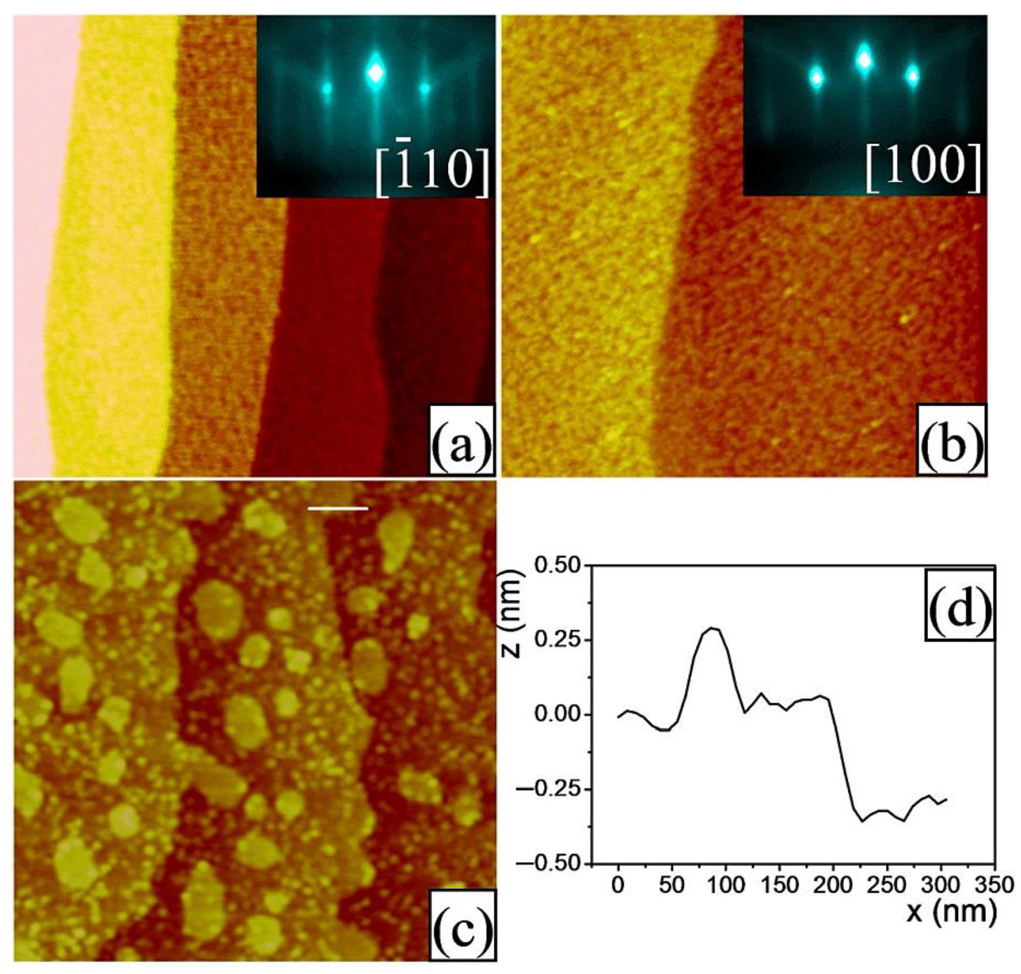
- The wetting of the substrate’s surface with either NdO1+x or GaO2−x termination was determined by hetero-epitaxial growth of one-unit-cell-thick TiO2, SrO or BaO layers by means of PLD on the annealed or chemically treated substrates. The amount of deposited material was less than (but close to) one monolayer in order to prevent the formation of precipitates [2,53]. The deposition conditions for each oxide are provided in Table 2. All targets were single crystals. First, TiO2 was deposited on an annealed (110) NdGaO3 surface. Figure 6a illustrates the AFM and RHEED data of the resulting film surface. Regularly spaced terraces separated by ~0.4nm-height steps are visible. It can be concluded that TiO2 is wetting the NdO1+x on the surface forming an almost closed layer. The corresponding RHEED pattern indicates a highly ordered surface. Since a B-site oxide (e.g., TiO2) does not wet a B-site-terminated ABO3 surface [1,2,26,60] (e.g., a GaO2−x terminated NdGaO3), it can be concluded that the annealed NdGaO3 substrate features a NdO1+x termination, thereby confirming the results from Ref. [36].
SrO was next deposited on an m-BHF etched (001) NdGaO3 surface. The RHEED specular intensity exhibited clear oscillatory behavior, with the deposition being stopped close to the completion of one monolayer. The resulting surface morphology and the corresponding RHEED pattern of the film are given in Figure 6b. The AFM micrograph revealed a smooth surface with one-unit-cell-height steps, while the RHEED pattern was characterized by sharp Bragg diffraction spots indicating a well-defined surface. The surface wetting was therefore complete, giving rise to an almost closed layer. Similar results were obtained for BaO (instead of SrO) deposited on chemically treated NdGaO3 substrates, with either (110) or (001) orientation, suggesting that the chemically and/or thermally treated NdGaO3 substrates are characterized by different terminations. When MeO films are grown on an annealed NdGaO3 surface, their surface wetting is incomplete, as shown in Figure 6c,d for the case of SrO, with the formation of SrO islands, indicating a different surface composition than for the annealed substrates. However, selective nucleation depends not only on the composition and type of metal oxide of the substrate terminating layer, but also on specific growth conditions, such as the gas pressure, substrate temperature, laser repetition rate and fluence [44,51]. The deposition of one monolayer of different metal oxides can also be used to switch the substrate termination to a desired composition [61].
4. Conclusions
A chemical-etching method developed to reproducibly obtain (110) or (001) NdGaO3 substrates with a predominant GaO2−x termination was described in this paper. By considering the layered structure of the substrate, the selective removal of one of the surface oxides (i.e., NdO1+x) was achieved by using modified commercial buffered HF solutions, adapted to the substrate’s characteristics (e.g., crystal orientation, miscut angle and its orientation with respect to the crystallographic axes). Proper chemical etching followed by high-temperature thermal treatment, in air or O2 flow, resulted in structurally and chemically well-defined surfaces, atomically flat and free of etch pits. For the experimental conditions used in this paper, the surface of the chemically etched substrates showed a lower free surface energy compared to that of the annealed ones.
Funding
This work was funded by the Dutch Science Foundation (Stichting voor Fundamenteel Onderzoek der Materie).
Institutional Review Board Statement
Not applicable.
Informed Consent Statement
Not applicable.
Data Availability Statement
Data are contained within the article.
Acknowledgments
This work was performed at Faculty of Science and Technology, MESA+ Institute for Nanotechnology, University of Twente, Enschede, The Netherlands. Continuous support from Guus Rijnders and Dave Blank during the period of performing the studies described here is kindly acknowledged.
Conflicts of Interest
The author declares no conflict of interest.
References
- Koster, G.; Rijnders, G.; Blank, D.H.A.; Rogalla, H. Surface morphology determined by (001) single-crystal SrTiO3 termination. Phys. C Supercond. 2000, 339, 215–230. [Google Scholar] [CrossRef]
- Huijbregtse, J.M.; Rector, J.H.; Dam, B. Effect of the two (100) SrTiO3 substrate terminations on the nucleation and growth of YBa2Cu3O7−δ thin films. Phys. C Supercond. 2001, 351, 183–199. [Google Scholar] [CrossRef]
- Matsumoto, Y.; Ohsawa, T.; Takahashi, R.; Koinuma, H. Surface termination effect on the photocatalysis on atomically controlled SrTiO3(001) surface. Thin Solid Films 2005, 486, 11–14. [Google Scholar] [CrossRef]
- Leca, V.; Blank, D.; Rijnders, G.; Bals, S.; van Tendeloo, G. Superconducting single-phase Sr1−xLaxCuO2 thin films with improved crystallinity grown by pulsed laser deposition. Appl. Phys. Lett. 2006, 89, 092504. [Google Scholar] [CrossRef]
- Guo, R.; Bhalla, A.S.; Cross, L.E.; Roy, R. Surface crystallographic structure compatibility between substrates and high Tc (YBCO) thin films. J. Mater. Res. 1994, 9, 1644–1656. [Google Scholar] [CrossRef]
- Koster, G.; Kropman, B.L.; Rijnders, G.J.H.M.; Blank, D.H.A.; Rogalla, H. Influence of the surface treatment on the homoepitaxial growth of SrTiO3. Mater. Sci. Eng. B 1998, 56, 209–212. [Google Scholar] [CrossRef]
- Phillips, J.M. Substrate selection for high-temperature superconducting thin films. J. Appl. Phys. 1996, 79, 1829–1848. [Google Scholar] [CrossRef]
- Vailionis, A.; Boschker, H.; Siemons, W.; Houwman, E.P.; Blank, D.H.A.; Rijnders, G.; Koster, G. Misfit strain accommodation in epitaxial ABO3 perovskites: Lattice rotations and lattice modulations. Phys. Rev. B 2011, 83, 64101. [Google Scholar] [CrossRef] [Green Version]
- Chakhalian, J.; Freeland, J.W.; Habermeier, H.-U.; Cristiani, G.; Khaliullin, G.; van Veenendaal, M.; Keimer, B. Orbital reconstruction and covalent bonding at an oxide interface. Science 2007, 318, 1114–1117. [Google Scholar] [CrossRef] [Green Version]
- Huijben, M.; Rijnders, G.; Blank, D.H.A.; Bals, S.; Van Aert, S.; Verbeeck, J.; Van Tendeloo, G.; Brinkman, A.; Hilgenkamp, H. Electronically coupled complementary interfaces between perovskite band insulators. Nat. Mater. 2006, 5, 556–560. [Google Scholar] [CrossRef]
- Koren, G.; Gupta, A.; Giess, E.; Segmuller, A.; Laibowitz, R. Epitaxial films of YBa2Cu3O7-δ on NdGaO3, LaGaO3, and SrTiO3 substrates deposited by laser ablation. Appl. Phys. Lett. 1989, 54, 1054–1056. [Google Scholar] [CrossRef]
- Balestrino, G.; Desfeux, R.; Martellucci, S.; Paoletti, A.; Petrocelli, G.; Tebano, A.; Mercey, B.; Hervieu, M. Growth of CaCuO2 and SrxCa1-xCuO2 epitaxial films on NdGaO3 substrates by pulsed laser deposition. J. Mater. Chem. 1995, 5, 1879–1883. [Google Scholar] [CrossRef]
- Li, K.; Qi, Z.; Li, X.; Zhu, J.; Zhang, Y. Growth, structural characteristics and magnetoresistance in LaCaMnO thin films prepared by dc magnetron sputtering. Thin Solid Films 1997, 304, 386–391. [Google Scholar] [CrossRef]
- Okazaki, H.; Arakawa, A.; Asahi, T.; Oda, O.; Aiki, K. GaN epitaxial growth on neodium gallate substrates. Solid. State. Electron. 1997, 41, 263–266. [Google Scholar] [CrossRef]
- Madhavan, S.; Mitchell, J.A.; Nemoto, T.; Wozniak, S.; Liu, Y.; Schlom, D.G.; Dabkowski, A.; Dabkowska, H.A. Growth of epitaxial Sr2RuO4 films and YBa2Cu3O7−δSr2RuO4 heterostructures. J. Cryst. Growth 1997, 174, 417–423. [Google Scholar] [CrossRef]
- Cao, L.; Zegenhagen, J.; Sozontov, E. The effect of epitaxial strain on RBa2Cu3O7 thin films and the perovskite substrate. Phys. C 2000, 337, 24–30. [Google Scholar] [CrossRef]
- Wördenweber, R.; Schwarzkopf, J.; Hollmann, E.; Duk, A.; Cai, B.; Schmidbauer, M. Impact of compressive in-plane strain on the ferroelectric properties of epitaxial NaNbO3 films on (110) NdGaO3. Appl. Phys. Lett. 2013, 103, 132908. [Google Scholar] [CrossRef]
- Wang, Y.; Chen, W.; Wang, B.; Zheng, Y. Ultrathin Ferroelectric Films: Growth, Characterization, Physics and Applications. Materials 2014, 7, 6377–6485. [Google Scholar] [CrossRef]
- Biegalski, M.D.; Qiao, L.; Gu, Y.; Mehta, A.; He, Q.; Takamura, Y.; Borisevich, A.; Chen, L.-Q. Impact of symmetry on the ferroelectric properties of CaTiO3 thin films. Appl. Phys. Lett. 2015, 106, 162904. [Google Scholar] [CrossRef] [Green Version]
- Schlom, D.G.; Chen, L.-Q.; Eom, C.-B.; Rabe, K.M.; Streiffer, S.K.; Triscone, J.-M. Strain Tuning of Ferroelectric Thin Films. Annu. Rev. Mater. Res. 2007, 37, 589–626. [Google Scholar] [CrossRef]
- Schwarzkopf, J.; Braun, D.; Hanke, M.; Uecker, R.; Schmidbauer, M. Strain Engineering of Ferroelectric Domains in KxNa1−xNbO3 Epitaxial Layers. Front. Mater. 2017, 4, 26. [Google Scholar] [CrossRef] [Green Version]
- Sharma, Y.; Agarwal, R.; Phatak, C.; Kim, B.; Jeon, S.; Katiyar, R.S.; Hong, S. Long-range Stripe Nanodomains in Epitaxial (110) BiFeO3 Thin Films on (100) NdGaO3 Substrate. Sci. Rep. 2017, 7, 4857. [Google Scholar] [CrossRef] [PubMed] [Green Version]
- Zhang, H.; Pryds, N.; Park, D.-S.; Gauquelin, N.; Santucci, S.; Christensen, D.V.; Jannis, D.; Chezganov, D.; Rata, D.A.; Insinga, A.R.; et al. Atomically engineered interfaces yield extraordinary electrostriction. Nature 2022, 609, 695–700. [Google Scholar] [CrossRef]
- Li, F.; Jin, L.; Xu, Z.; Zhang, S. Electrostrictive effect in ferroelectrics: An alternative approach to improve piezoelectricity. Appl. Phys. Rev. 2014, 1, 11103. [Google Scholar] [CrossRef] [Green Version]
- Rogdakis, K.; Seo, J.W.; Viskadourakis, Z.; Wang, Y.; Ah Qune, L.F.N.; Choi, E.; Burton, J.D.; Tsymbal, E.Y.; Lee, J.; Panagopoulos, C. Tunable ferroelectricity in artificial tri-layer superlattices comprised of non-ferroic components. Nat. Commun. 2012, 3, 1064. [Google Scholar] [CrossRef] [PubMed] [Green Version]
- Koster, G. Artificially Layered Oxides by Pulsed Laser Deposition; University of Twente: Enschede, The Netherlands, 1999. [Google Scholar]
- Utke, I.; Klemenz, C.; Scheel, H.J.; Sasaura, M.; Miyazawa, S. Misfit problems in epitaxy of high-Tc superconductors. J. Cryst. Growth 1997, 174, 806–812. [Google Scholar] [CrossRef]
- Vasylechko, L.; Matkovskii, A.; Savytskii, D.; Suchocki, A.; Wallrafen, F. Crystal structure of GdFeO3-type rare earth gallates and aluminates. J. Alloys Compd. 1999, 291, 57–65. [Google Scholar] [CrossRef]
- Marti, W.; Fischer, P.; Altorfer, F.; Scheel, H.J.; Tadin, M. Crystal structures and phase transitions of orthorhombic and rhombohedral RGaO3(R=La,Pr,Nd) investigated by neutron powder diffraction. J. Phys. Condens. Matter 1994, 6, 127–135. [Google Scholar] [CrossRef]
- Vasylechko, L.; Akselrud, L.; Morgenroth, W.; Bismayer, U.; Matkovskii, A.; Savytskii, D. The crystal structure of NdGaO3 at 100 K and 293 K based on synchrotron data. J. Alloys Compd. 2000, 297, 46–52. [Google Scholar] [CrossRef]
- Gunkel, F.; Skaja, K.; Shkabko, A.; Dittmann, R.; Hoffmann-Eifert, S.; Waser, R. Stoichiometry dependence and thermal stability of conducting NdGaO3/SrTiO3 heterointerfaces. Appl. Phys. Lett. 2013, 102, 71601. [Google Scholar] [CrossRef]
- Wade, K.; Banister, A.J. Comprehensive Inorganic Chemistry; Oxford Pergamon Press: London, UK, 1973. [Google Scholar]
- Gao, G.; Yin, Z.; Huang, Z.; Jin, S.; Wu, W. The thickness evolution of orthorhombic lattice distortions in heteroepitaxial La0.67Ca0.33MnO3/NdGaO3(110)Or observed by X-ray reciprocal space mapping. J. Phys. D Appl. Phys. 2008, 41, 152001. [Google Scholar] [CrossRef]
- Hirata, A.; Ando, A.; Saiki, K.; Koma, A. Characterization of surface defects formation in strontium titanate(100). Surf. Sci.–Surf. SCI 1994, 310, 89–94. [Google Scholar] [CrossRef]
- Ikeda, A.; Nishimura, T.; Morishita, T.; Kido, Y. Surface relaxation and rumpling of TiO2-terminated SrTiO3(001) determined by medium energy ion scattering. Surf. Sci.–Surf. SCI 1999, 433, 520–524. [Google Scholar] [CrossRef]
- Ohnishi, T.; Takahashi, K.; Nakamura, M.; Kawasaki, M.; Yoshimoto, M.; Koinuma, H. A-site layer terminated perovskite substrate: NdGaO3. Appl. Phys. Lett. 1999, 74, 2531–2533. [Google Scholar] [CrossRef]
- Kwon, C.; Li, Q.; Xi, X.; Bhattacharya, S.; Doughty, C.; Venkatesan, T.; Zhang, H.; Lynn, J.; Peng, J.; Li, Z.; et al. High critical current densities in ultrathin YBa2Cu3O7-δ films sandwiched between (PrxY1-x)Ba2Cu3O7-δ layers. Appl. Phys. Lett. 1993, 62, 1289–1291. [Google Scholar] [CrossRef]
- Sum, R.; Lang, H.P.; Güntherodt, H.-J. Scanning force microscopy study of single-crystal substrates used for thin-film growth of high-temperature superconductors. Phys. C Supercond. 1995, 242, 174–182. [Google Scholar] [CrossRef]
- Dirsyte, R.; Schwarzkopf, J.; Wagner, G.; Lienemann, J.; Busch, M.; Winter, H.; Fornari, R. Surface termination of the NdGaO3(110). Appl. Surf. Sci. 2009, 255, 8685–8687. [Google Scholar] [CrossRef]
- Cavallaro, A.; Harrington, G.F.; Skinner, S.J.; Kilner, J.A. Controlling the surface termination of NdGaO3(110): The role of the gas atmosphere. Nanoscale 2014, 6, 7263–7273. [Google Scholar] [CrossRef] [PubMed]
- Leca, V. Heteroepitaxial Growth of Copper Oxide Superconductors by Pulsed Laser Deposition; University of Twente: Enschede, The Netherlands, 2003. [Google Scholar]
- Leca, V.; Rijnders, G.; Koster, G.; Blank, D.H.A.; Rogalla, H. Wet Etching Methods for Perovskite Substrates. MRS Proc. 1999, 587, O3.6. [Google Scholar] [CrossRef]
- Leca, V.; Andronescu, E. Improved surface morphology of (110) NdGaO3 substrates by thermal and chemical treatments. Rom. J. Mater. 2011, 41, 127. [Google Scholar]
- Kleibeuker, J.E.; Koster, G.; Siemons, W.; Dubbink, D.; Kuiper, B.; Blok, J.L.; Yang, C.-H.; Ravichandran, J.; Ramesh, R.; ten Elshof, J.E.; et al. Atomically Defined Rare-Earth Scandate Crystal Surfaces. Adv. Funct. Mater. 2010, 20, 3490–3496. [Google Scholar] [CrossRef]
- Biswas, A.; Yang, C.-H.; Ramesh, R.; Jeong, Y.H. Atomically flat single terminated oxide substrate surfaces. Prog. Surf. Sci. 2017, 92, 117–141. [Google Scholar] [CrossRef] [Green Version]
- Polli, A.D.; Wagner, T.; Rühle, M. Effect of Ca impurities and wet chemical etching on the surface morphology of SrTiO3 substrates. Surf. Sci. 1999, 429, 237–245. [Google Scholar] [CrossRef]
- Kawasaki, M.; Takahashi, K.; Maeda, T.; Tsuchiya, R.; Shinohara, M.; Ishiyama, O.; Yonezawa, T.; Yoshimoto, M.; Koinuma, H. Atomic Control of the SrTiO3 Crystal Surface. Science 1994, 266, 1540–1542. [Google Scholar] [CrossRef] [PubMed]
- Kawasaki, M.; Ohtomo, A.; Arakane, T.; Takahashi, K.; Yoshimoto, M.; Koinuma, H. Atomic control of SrTiO3 surface for perfect epitaxy of perovskite oxides. Appl. Surf. Sci. 1996, 107, 102–106. [Google Scholar] [CrossRef]
- Lippmaa, M.; Takahashi, K.; Ohtomo, A.; Ohashi, S.; Ohnishi, T.; Nakagawa, N.; Sato, T.; Iwatsuki, M.; Koinuma, H.; Kawasaki, M. Atom technology for Josephson tunnel junctions: SrTiO3 substrate surface. Mater. Sci. Eng. B 1998, 56, 111–116. [Google Scholar] [CrossRef]
- Koster, G.; Kropman, B.L.; Rijnders, G.J.H.M.; Blank, D.H.A.; Rogalla, H. Quasi-ideal strontium titanate crystal surfaces through formation of strontium hydroxide. Appl. Phys. Lett. 1998, 73, 2920–2922. [Google Scholar] [CrossRef] [Green Version]
- Kleibeuker, J.E.; Kuiper, B.; Harkema, S.; Blank, D.H.A.; Koster, G.; Rijnders, G.; Tinnemans, P.; Vlieg, E.; Rossen, P.B.; Siemons, W.; et al. Structure of singly terminated polar DyScO3 (110) surfaces. Phys. Rev. B 2012, 85, 165413. [Google Scholar] [CrossRef] [Green Version]
- Liu, G.; Wang, H.; Makino, H.; Ko, H.-J.; Hanada, T.; Yao, T. Growth of PrSrMnO3-like thin films on NGO (110) substrates by plasma assisted MBE. J. Cryst. Growth 2001, 227–228, 960–965. [Google Scholar] [CrossRef]
- Gagnidze, T.; Ma, H.; Cancellieri, C.; Bona, G.-L.; Mattina, F. La Structural properties of ultrathin SrO film deposited on SrTiO3. Sci. Technol. Adv. Mater. 2019, 20, 456–463. [Google Scholar] [CrossRef] [Green Version]
- Kikyuama, H.; Miki, N.; Saka, K.; Takano, J.; Kawanabe, I.; Miyashita, M.; Ohmi, T. Principles of wet chemical processing in ULSI microfabrication. IEEE Trans. Semicond. Manuf. 1991, 4, 26–35. [Google Scholar] [CrossRef]
- Kikuyama, H.; Waki, M.; Miyashita, M.; Yabune, T.; Miki, N.; Takano, J.; Ohmi, T. A Study of the Dissociation State and the SiO2 Etching Reaction for HF Solutions of Extremely Low Concentration. J. Electrochem. Soc. 1994, 141, 366. [Google Scholar] [CrossRef]
- Stäuble-Pümpin, B.; Ilge, B.; Matijasevic, V.C.; Scholte, P.M.L.O.; Steinfort, A.J.; Tuinstra, F. Atomic force microscopy study of (001) SrTiO3 surfaces. Surf. Sci. 1996, 369, 313–320. [Google Scholar] [CrossRef]
- Senapati, L.; Sharma, R.; Venkatesan, T.; Zhang, Z.; Chu, W.-K. Ion channeling studies of regrowth kinetics in crystalline metal oxides used with high temperature superconductors. Appl. Phys. Lett. 1996, 68, 123–125. [Google Scholar] [CrossRef]
- Rijnders, G.J.H.M.; Koster, G.; Blank, D.H.A.; Rogalla, H. In Situ monitoring during pulsed laser deposition of complex oxides using reflection high energy electron diffraction under high oxygen pressure. Appl. Phys. Lett. 1997, 70, 1888–1890. [Google Scholar] [CrossRef]
- Fompeyrine, J.; Berger, R.; Lang, H.P.; Perret, J.; Mächler, E.; Gerber, C.; Locquet, J.-P. Local determination of the stacking sequence of layered materials. Appl. Phys. Lett. 1998, 72, 1697–1699. [Google Scholar] [CrossRef]
- Tsuchiya, R.; Kawasaki, M.; Kubota, H.; Nishino, J.; Sato, H.; Akoh, H.; Koinuma, H. YBa2Cu3O7−δ trilayer junction with nm thick PrGaO3 barrier. Appl. Phys. Lett. 1997, 71, 1570–1572. [Google Scholar] [CrossRef]
- Baeumer, C.; Xu, C.; Gunkel, F.; Raab, N.; Heinen, R.A.; Koehl, A.; Dittmann, R. Surface Termination Conversion during SrTiO3 Thin Film Growth Revealed by X-ray Photoelectron Spectroscopy. Sci. Rep. 2015, 5, 11829. [Google Scholar] [CrossRef]
Figure 1.
AFM topographic images: (a) as-received (110) NdGaO3 substrate, annealed for 0.5 h at 550 °C under O2 flow (100 L/h), showing a non-terraced structure; (b) the RHEED pattern corresponding to the substrate from (a); (c) (110) NdGaO3 substrate annealed in air for 1 h at 1000 °C; (d) (001) NdGaO3 substrate after 0.5 min of chemical etching in commercial BHF solution, followed by annealing at 1000 °C for 2 h, under O2 flow (200 L/h). The scan line profile from (e) indicates trenches approximately 0.2nm-deep. AFM scans size: (a) 4 × 4 μm2, (c) 1.25 × 1.25 μm2, (d) 5 × 5 μm2.

Figure 2.
(a,b) AFM topographic images, (c) the line scan profile of image (a), and (d) the corresponding RHEED pattern for a (110) NdGaO3 substrate chemically etched for 0.5 min (m-BHF solution, pH = 5.5), followed by annealing for 2 h at 1000 °C in O2 flow (100 L/h). AFM scans size: (a) 1 × 1 μm2 and (b) 7 × 7 μm2 (from Ref. [29]).
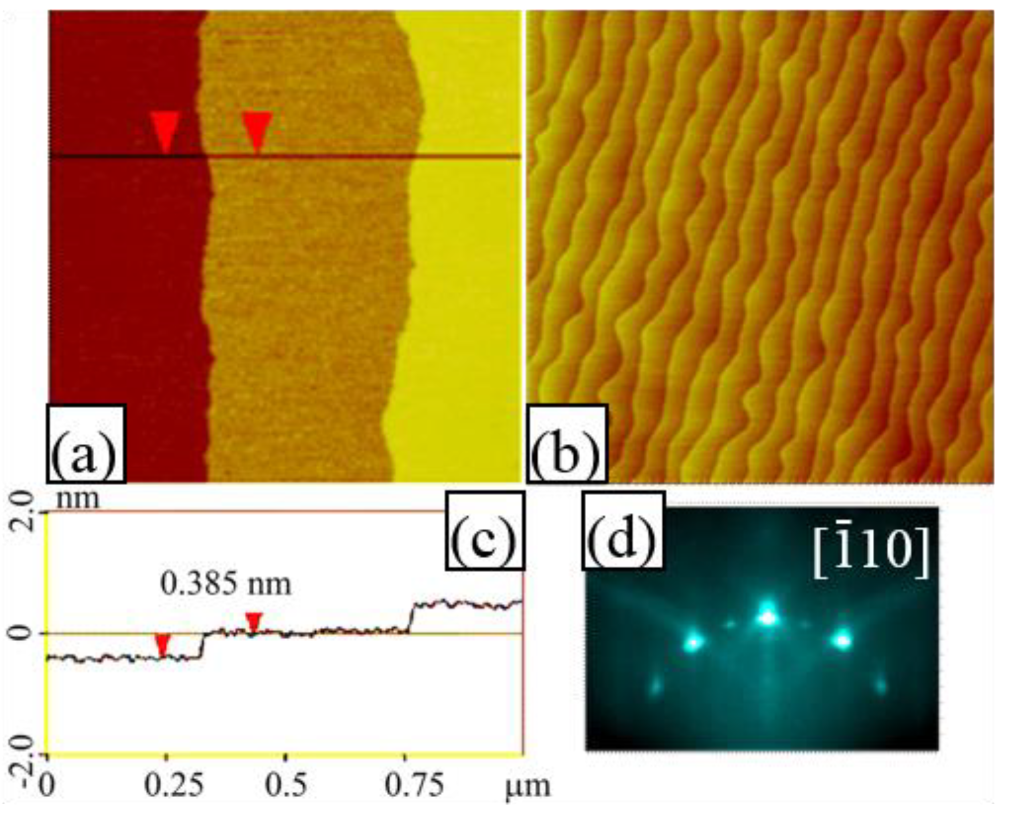
Figure 3.
(a) Topographic AFM image, (b) the line scan profiles, and (c) the RHEED pattern of the substrate from (a) for a (001) NdGaO3 substrate chemically etched for 2 min (m-BHF solution, pH = 4.5), followed by annealing for 2 h at 1000 °C in O2 flow (200 L/h). AFM scans size: 3 × 3 μm2 (from Ref. [29]).
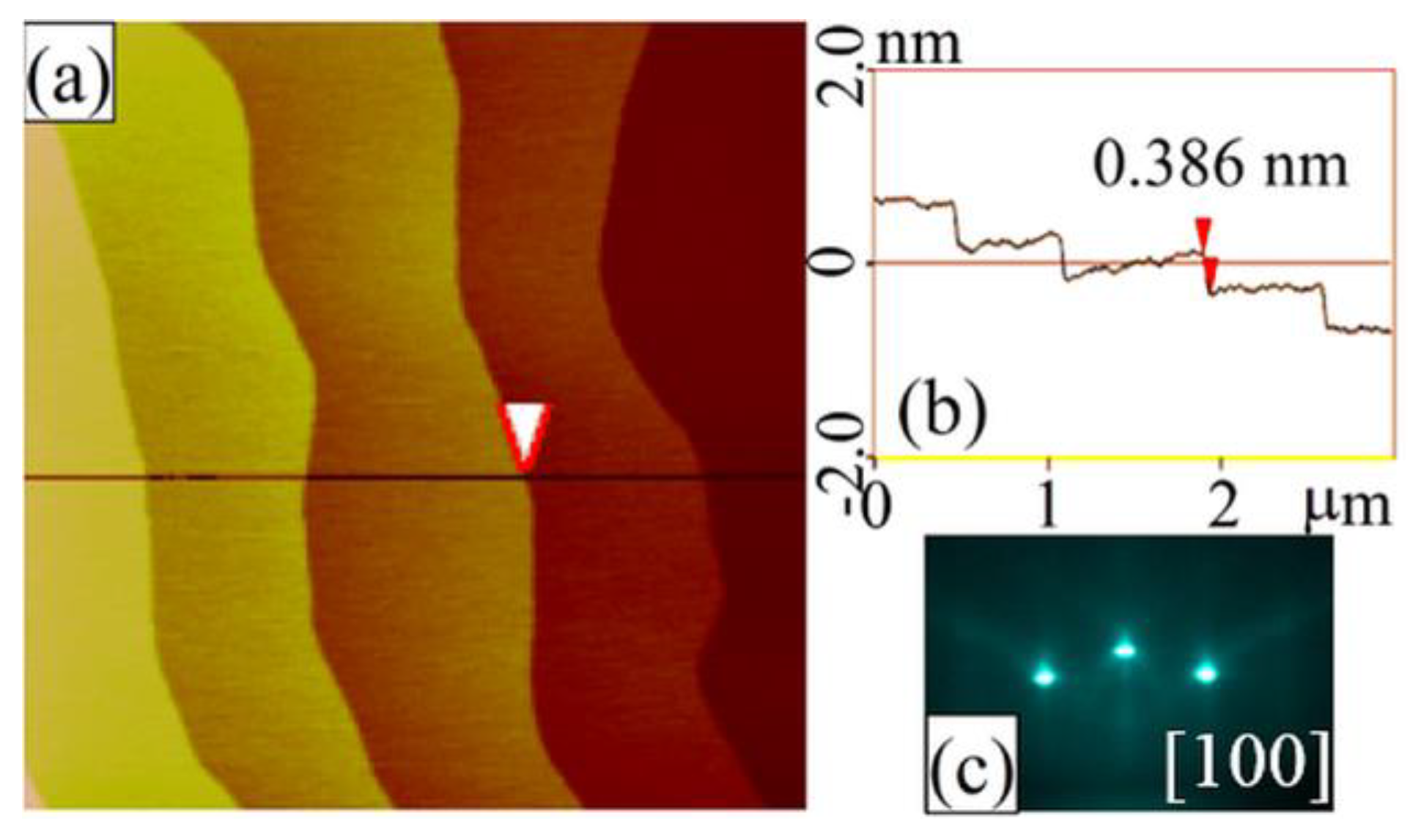
Figure 4.
(a,c) Topographic AFM images and (b,c) the line scan profiles indicating incomplete etching (a,b) and etch pit formation (c,d) for: (001) NdGaO3 substrate chemically etched for 2 min (m-BHF solution, pH = 5.5), in (a,b); (110) NdGaO3 substrate chemically etched for 2 min (m-BHF solution, pH = 4.5), in (c and d). Chemical etching was followed by annealing for 2 h at 1000 °C in O2 flow (200 L/h). AFM scans size: (a) 5 × 5 μm2 and (c) 2.5 × 2.5 μm2.

Figure 5.
AFM images of (001) NdGaO3 substrates (cut from the same larger wafer) characterized by an angle Δ of 45°: (a) chemically etched for 2 min in m-BHF solution and annealed for 2 h at 1000 °C in air, (b) only annealed for 2 h at 1000 °C in air. AFM scans size: (a) 7 × 7 μm2, and (b) 5 × 5 μm2.
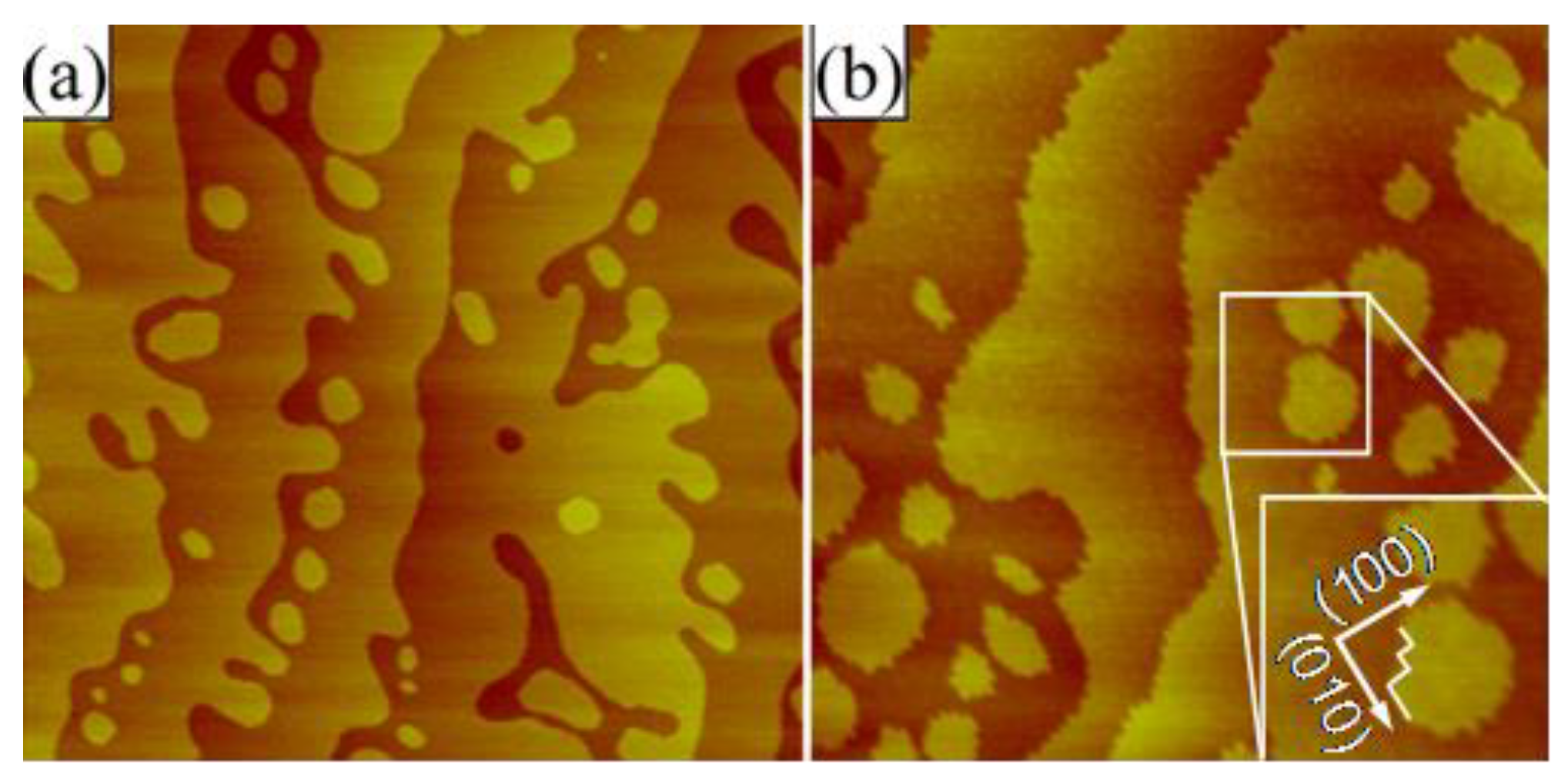
Figure 6.
AFM topographic images and the corresponding RHEED patterns of (a) ~1 monolayer TiO2 deposited on (110) NdGaO3 substrate annealed for 1 h at 1000 °C in O2 flow (50 L/h); (b) ~1 monolayer SrO deposited on (001) NdGaO3 substrate chemically etched in m-BHF solution and then annealed for 2 h at 1000 °C, in O2 flow (200 L/h); (c) SrO (the same amount of material as in (b)) deposited on (001) NdGaO3 substrate annealed for 2 h at 1000 °C, in O2 flow (200 L/h); SrO islands of about 0.26 nm height formed in this case on substrate terraces (cpc height), as shown by the line scan from (d). AFM scan size: (a) 1.5 × 1.5 μm2, (b) 0.75 × 0.75 μm2, and (c) 2 × 2 μm2.

Table 1.
Room temperature structural and physical properties of bulk NdGaO3. mp = melting point, ε = dielectric constant, ⍴ = density, tan δ = dielectric loss, α = linear thermal expansion coefficient.
Table 1.
Room temperature structural and physical properties of bulk NdGaO3. mp = melting point, ε = dielectric constant, ⍴ = density, tan δ = dielectric loss, α = linear thermal expansion coefficient.
| Symmetry | Space Group | Unit Cell (Å) | mp (°C) | ε | ⍴ (g/cm3) | tan δ | α (K−1) |
|---|---|---|---|---|---|---|---|
| Orthorhombic, GdFeO3 type | Pbnm | ao = 5.428 bo = 5.498 co = 7.708 | 1605 | 20–25 (1 MHz) | 7.57 | 3 × 10⁻³ | 5.8 × 10⁻⁶ |
Table 2.
Deposition parameters for the MeO (Me = Ti, Sr, Ba) thin films. Td = deposition temperature, Pd = deposition pressure (O2 gas), Ed = laser energy density on target, f = laser repetition rate, dts = substrate–target distance.
Table 2.
Deposition parameters for the MeO (Me = Ti, Sr, Ba) thin films. Td = deposition temperature, Pd = deposition pressure (O2 gas), Ed = laser energy density on target, f = laser repetition rate, dts = substrate–target distance.
| Material | Td (°C) | Pd (Pa) | Ed (J/cm2) | f (Hz) | dst (mm) |
|---|---|---|---|---|---|
| TiO2 | 850 | 7.5 | 2 | 1 | 45 |
| SrO | 750 | 10 | 2 | 1 | 55 |
| BaO | 590 | 15 | 1.3 | 1 | 55 |
Publisher’s Note: MDPI stays neutral with regard to jurisdictional claims in published maps and institutional affiliations. |
© 2022 by the author. Licensee MDPI, Basel, Switzerland. This article is an open access article distributed under the terms and conditions of the Creative Commons Attribution (CC BY) license (https://creativecommons.org/licenses/by/4.0/).
Share and Cite
MDPI and ACS Style
Leca, V. Termination Control of (001) and (110) NdGaO3 Single-Crystal Substrates by Selective Chemical Etching. Crystals 2022, 12, 1791. https://doi.org/10.3390/cryst12121791
AMA Style
Leca V. Termination Control of (001) and (110) NdGaO3 Single-Crystal Substrates by Selective Chemical Etching. Crystals. 2022; 12(12):1791. https://doi.org/10.3390/cryst12121791
Chicago/Turabian StyleLeca, Victor. 2022. "Termination Control of (001) and (110) NdGaO3 Single-Crystal Substrates by Selective Chemical Etching" Crystals 12, no. 12: 1791. https://doi.org/10.3390/cryst12121791
Note that from the first issue of 2016, this journal uses article numbers instead of page numbers. See further details here.