
Progress of InGaN-Based Red Micro-Light Emitting Diodes
by
 and
and
Panpan Li
1, 
Hongjian Li
1,*,
Matthew S. Wong
1,
Philip Chan
1,
Yunxuan Yang
1,
Haojun Zhang
1,
Mike Iza
1,
James S. Speck
1,
Shuji Nakamura
1,2 and
Steven P. Denbaars
1,2 1
Materials Department, University of California, Santa Barbara, CA 93106, USA
2
Department of Electrical and Computer Engineering, University of California, Santa Barbara, CA 93117, USA
*
Author to whom correspondence should be addressed.
Crystals 2022, 12(4), 541; https://doi.org/10.3390/cryst12040541
Submission received: 29 March 2022
/
Revised: 10 April 2022
/
Accepted: 10 April 2022
/
Published: 12 April 2022
(This article belongs to the Special Issue III-Nitride-Based Light-Emitting Devices)
Abstract
:InGaN-based red micro-size light-emitting diodes (μLEDs) have become very attractive. Compared to common AlInGaP-based red µLEDs, the external quantum efficiency (EQE) of InGaN red µLEDs has less influence from the size effect. Moreover, the InGaN red µLEDs exhibit a much more robust device performance even operating at a high temperature of up to 400 K. We review the progress of InGaN red μLEDs. Novel growth methods to relax the strain and increase the growth temperature of InGaN red quantum wells are discussed.
1. Introduction
Micro-size light-emitting diodes (μLEDs) have attracted huge attention as the next-generation display technology for wide applications, such as wearable watches, virtual/augmented reality, micro-projectors, and ultra-large televisions [1,2,3,4]. InGaN-based red μLEDs have become the research focus now [5,6,7,8]. To achieve red emission, the indium composition in the InGaN quantum wells (QWs) should be greater than 35%, which causes a lot of challenges. First, the large lattice mismatch leads to a high defect density. Second, a much lower growth temperature is required to increase the indium incorporation efficiency in the InGaN red QWs, resulting in poor materials crystal quality. Moreover, the high indium composition InGaN red QWs generate a large piezoelectric field and severe quantum-confinement Stark effect (QCSE), leading to a poor internal quantum efficiency (IQE) [8]. The common AlInGaP-based red light-emitting diodes (LEDs) show high efficiency in regular size devices (0.1 mm2) but the μLEDs devices suffer from a severe size-effect in external quantum efficiency (EQE) and poor thermal stability at a high temperature [9,10,11,12]. Our group has demonstrated that InGaN μLEDs can overcome EQE size effect by proper sidewalls passivation/treatment. InGaN μLEDs also exhibit a robust thermal stability in commercial InGaN blue and green LEDs [6,13,14]. Therefore, InGaN red μLEDs are promising candidates for μLEDs display application.
Our group has reported high efficiency InGaN green LEDs using AlGaN cap layer grown on top of InGaN green QWs [15]. More recently, we reported InGaN red μLEDs with an EQE over 3% using similar active region design [5,6,7]. Other novel growth strategies have been proposed to achieve InGaN red μLEDs, such as InGaNOS pseudo-substrate [16,17,18,19], nano-porous GaN [20], strain relaxed InGaN buffer layer using in-situ InGaN decomposition layer [21,22]. These technologies aim to relax the strain of InGaN buffer layer and increase the indium intake efficiency in the red InGaN QWs. Thus, the red InGaN QWs can be grown at a higher temperature, which promises a high crystal quality. Moreover, a new model of 3-dimension “V” pits injections was proposed and high-efficiency InGaN red LEDs were reported [23,24].
In this review, we discuss the advantages of InGaN red μLEDs. We review the recent progress of InGaN red LEDs/μLEDs grown on all kinds of substrate/templates, such as patterned sapphire substrate (PSS), Si (111), InGaNOS, nano-porous GaN template, and strain relaxed InGaN layer.
2. Advantages of InGaN Red μLEDs
2.1. Size-Independent Peak EQE of InGaN Red μLEDs
The EQE of AlInGaP red µLEDs reduces dramatically by decreasing the device size. Ultra-small size AlInGaP red µLEDs show a much lower efficiency, which cannot meet the requirement of AR and VR applications. P. Li et al. from UCSB firstly demonstrated size-independent EQE in the InGaN red µLEDs. Figure 1a shows the uniform emission (~3 A/cm2) by optical microscopy images for the InGaN red µLEDs with size reduces from 100 × 100 to 20 × 20 μm2 [6]. These µLEDs show a packaged EQE varied from 2.4% to 2.6% as the size reduces from 100 × 100 to 20 × 20 μm2 (Figure 1). The emission wavelength is centered at 607 nm and the full-width half maximum (FWHM) is 50 nm. A comparison of normalized EQE vs. µLEDs size between InGaN and AlInGaP red µLEDs points out that the EQE of AlInGaP red µLEDs reduces dramatically as the size decreases to 20 × 20 μm2 (only 43% EQE left) [10]. This is caused by Shockley-Read-Hall (SRH) nonradiative recombination due to sidewalls damage and a higher surface recombination velocity. It is very difficult to overcome this challenge since it is related to the intrinsic AlInGaP materials property. In contrast, the EQE of InGaN red µLEDs has less influence from the size effect down to 20 × 20 μm2 due to a lower surface recombination velocity. For the size down to 20 × 20 μm2, the electroluminescence (EL) is very uniform in InGaN red µLEDs. It is promising to achieve ultra-small (<10 × 10 μm2) high-efficiency red µLEDs using InGaN materials system instead of the common AlInGaP materials.
2.2. Robust Temperature Property of InGaN Red μLEDs
The output power and EQE of AlInGaP red µLEDs decrease dramatically when the operation temperature gets higher [12]. This is caused by carrier leakage and injection efficiency reduction. In contrast, InGaN red µLEDs show a robust thermal property. P. Li et al. from UCSB investigated the high-temperature EL properties from 300 K to 400 K of InGaN red µLEDs (40 × 40 µm2) [7,14]. The 600 nm InGaN red µLEDs show a high peak EQE of 3.2%. From Figure 2, the peak EQE decreases as the temperature increases, especially at a low current density (J). The hot/cold factor (HC factor) was defined by the ratio of high-temperature EQE to room-temperature EQE to quantify the thermal droop. At 50 A/cm2, the EQE HC factor is as high as 0.85 at 360 K and 0.72 at 400 K. The high HC in InGaN red µLEDs agrees with commercial InGaN blue LEDs, which is a general property in the InGaN materials system. The thermal droop of output power in AlInGaP red µLEDs is much more severe. Lee et al. reported that the output power of AlInGaP red µLEDs was reduced by more than 70% as the operating temperature increased to 120 °C (~400 K) [12]. Therefore, InGaN red µLEDs is much more robust at a high temperature, making them more promising for AR and VR application.
3. Progress of InGaN Red LEDs and μLEDs
3.1. InGaN Red LEDs/μLEDs Grown on PSS
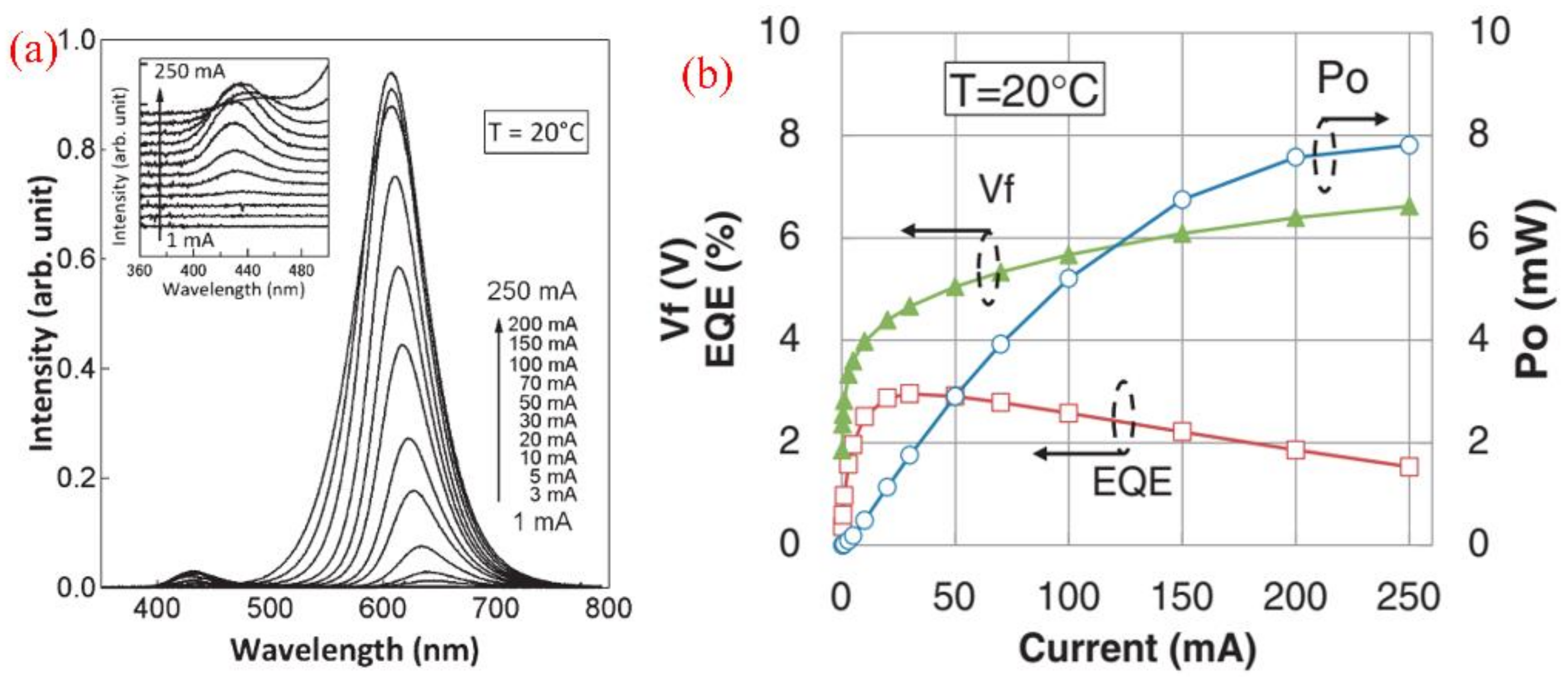
In 2014, Hwang et al. from Toshiba reported regular size (0001) InGaN red LEDs grown on PSS [8]. A high Al composition Al0.9Ga0.1N layer was inserted on top of InGaN red QWs, resulting in the uniform red emission from fluorescence images. From Figure 3, the 460 × 460 μm2 size InGaN red LEDs show an output power of 11 mW, an EQE of 2.9% and an emission wavelength of 629 nm at 20 mA. Another weak peak located at 430 nm was observed in the spectra, which is related to the phase-separated component in the InGaN red QWs.
In 2020, Iida et al. from KAUST reported InGaN red LEDs growing on PSS using 8-μm-thick n-GaN under layer with a lower residual in-plane stress. The red LEDs show a peak emission wavelength of 633 nm, a light output power of 0.64 mW, and external quantum efficiency of 1.6% at 20 mA [25]. Meanwhile, they demonstrated 10 × 10 arrays of InGaN 17 × 17 μm2 μLEDs [26]. The peak wavelength was blue-shifted from 662 to 630 nm as the J increased from 10 to 50 A/cm2. The on-wafer EQE was 0.18% at 50 A/cm2 and the output power density was 1.76 mW/mm2.
In 2021, Li et al. from UCSB demonstrated significant progress of InGaN red μLEDs on PSS [5,6,7]. As discussed in Section 2.1, the packaged 607 nm InGaN red μLEDs show a peak EQE of 2.4% to 2.6% as the size reduces from 100 × 100 μm2 to 20 × 20 μm2. The same team also demonstrated InGaN red μLEDs with a peak EQE of 3.2% and a much more robust thermal stability as compared to the common AlInGaP red μLEDs. Moreover, Li et al. from UCSB reported ultra-small 5 × 5 μm2 InGaN amber μLEDs grown on PSS with a peak EQE greater than 2% (Figure 4) [5]. The leakage current was only 10−9 A at −5 V. Since the AR and VR display demand μLEDs with a size smaller than 10 × 10 μm2, the excellent optical and electrical performance of the 5 × 5 μm2 InGaN amber μLEDs suggests the promising application for AR and VR micro-display using InGaN materials. The Light Tool simulation reveals that the light extraction efficiency (LEE) is 76% in the 5 × 5 μm2 InGaN red μLEDs, which is higher than 64% in the 100 × 100 μm2 μLEDs due to an enhanced light scatting from the sidewalls. However, the EQE of 5 × 5 μm2 InGaN μLEDs is lower than that of 100 × 100 μm2 μLEDs (3.2%). Therefore, the impact of nonradiative recombination from the sidewalls damage can’t be neglected in such small μLEDs. Fewer damage sidewalls etching process is a good approach to improve the efficiency of ultra-small InGaN red μLEDs. More recently, Li et al. from UCSB reported 623 nm red InGaN μLEDs (60 × 60 μm2) with a peak EQE of 4.5% using epitaxial tunnel junction (TJ) contact [27]. GaN TJ offers a better current spreading and less optical loss, which can improve efficiency. These EQE values are one order higher than the previous reports about InGaN red µLEDs and represent the start-of-the-are results for InGaN red μLEDs [17,19,20,21,22].
3.2. High-Efficiency InGaN Red LEDs Grown on Silicon Substrate Using 3-Dimension “V” Pits Injection
In 2019, Jiang et al. from Nanchang University proposed a “3D pn junction” from V-pits injection [23]. The V-pits can screen the dislocations and increase the hole injection into the active region. In 2020, the same team reported efficient InGaN-based red LEDs grown on Si (111) substrates [24]. The voids of V-pits reduce compressive strain and benefit the growth of high In composition InGaN QWs. The hybrid MQWs design with yellow QWs and orange QWs enables a high peak wall-plug efficiency (WPE) of 24% at 0.8 A/cm2 with an emission wavelength of 608 nm. 621 nm InGaN red LEDs with a peak WPE of 16.8% were achieved with a very low forward voltage of 1.96 V at 0.8 A/cm2. Theoretical simulation of “3D V-pits injection” has been investigated [28].
3.3. InGaN Red μLEDs Using Semi-Relaxed InGaNOS Pseudo-Substrate
In 2017, Even et al. from LETI and Soitec observed a significant enhancement of indium incorporation in full InGaN heterostructure grown on semi-relaxed InGaN pseudo-substrate (InGaNOS) due to the composition pulling effect [16]. The InGaNOS was developed by Soitec based on its Smart CutTM technology and offers a thin relaxed InGaN seed layer. The photoluminescent (PL) was red-shifted by ~50 nm by growing InGaN QWs on InGaNOS compared to the common GaN template (Figure 5). In 2021, Dussaigne et al. from LETI and Soitec reported InGaN red μLEDs grown on InGaNOS with a lattice parameter of 3.210 Å [17]. The 10 μm diameter circular 625 nm InGaN red μLEDs show an EQE of 0.14% at 8 A/cm2, despite the LEE estimated below 4%. Moreover, White et al. from UCSB and Soitec have greatly improved the EQE of 80 × 80 μm2 609 nm InGaN μLEDs on InGaNOS to 0.83% by reducing the defect density in the InGaN/GaN buffer layer and optimizing the p-type structure [18,19]. Noted that the growth temperature for red QWs on InGaNOS is much higher than the typical red QWs grown on GaN template (close to green InGaN QWs growth temperature).
3.4. InGaN Red μLEDs Grown on Strain Relaxed Nano-Porous InGaN Template
In 2021, Pasayat et al. from UCSB developed compliant GaN on porous GaN pseudo-substrates (PSs) for strain relaxed InGaN layer [20]. A 10 × 10 μm2 pattern with a 100 nm compliant GaN cap layer was grown on top of the porous GaN layer. Doping selective electrochemical (EC) etching was used to form the nano-porous structure. The 440 nm thick InGaN layer with 3–4% indium composition grown on the PSs shows a 56% strain relaxation from the X-ray diffraction reciprocal space map (RSM) (Figure 6). The peak wavelength was red-shifted by 56 nm. The 632 nm InGaN red μLEDs (6 × 6 μm2) show a peak on-wafer EQE of 0.2% (Figure 6). The output power density was 2.1 mW/mm2 at 100 A/cm2. However, such technology involves a complicated fabrication process and materials overgrowth. The thermal conductivity and reliability remain poor for the nano-porous template.
3.5. InGaN Red μLEDs Grown on Strained Relaxed Layer Using In-Situ Decomposition Layer
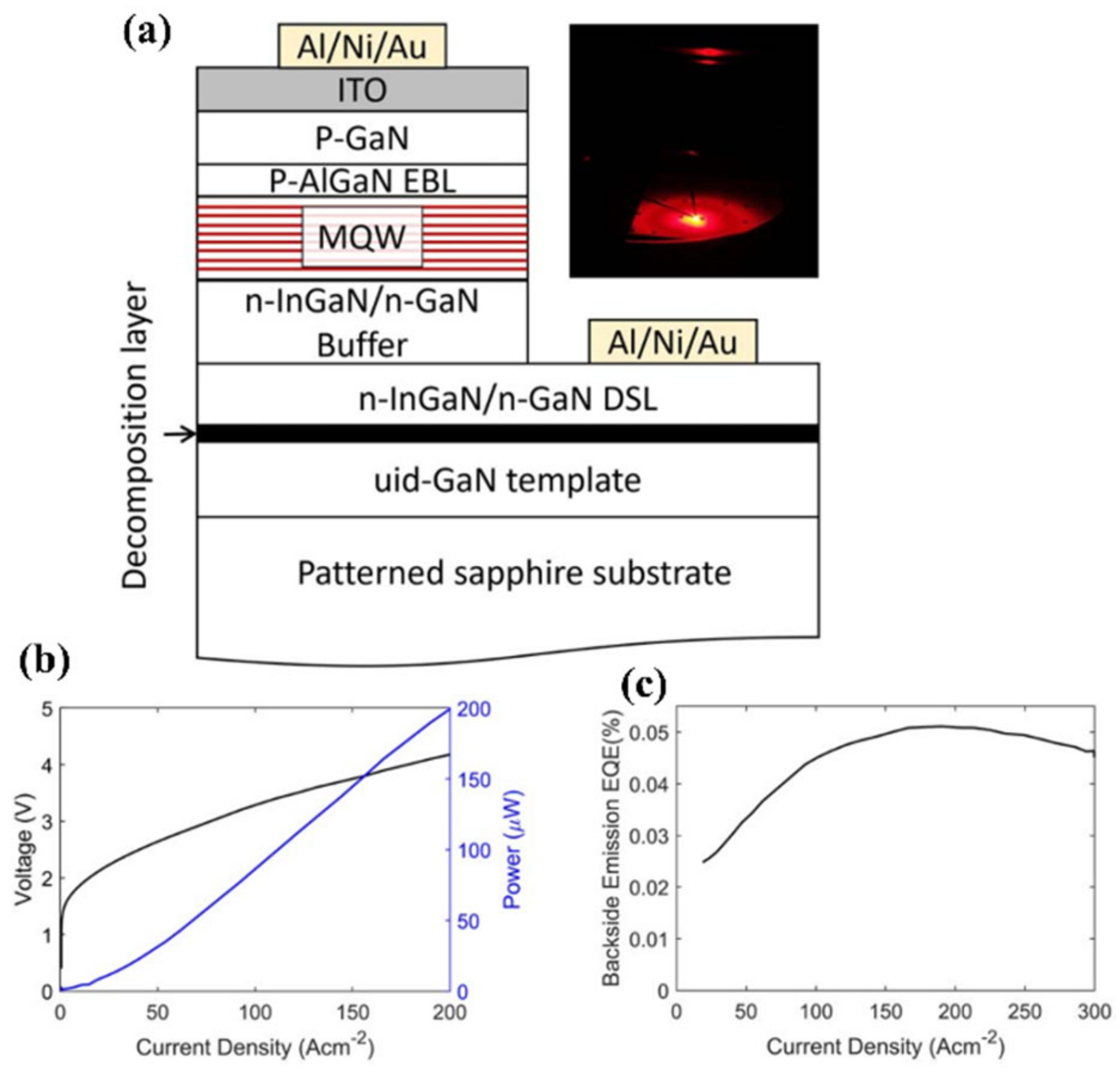
In 2021, Chan et al. from UCSB developed a novel technology using in-situ InGaN decomposition layer (DL) to achieve highly strain relaxed InGaN PSs [21]. A 3 nm thick very high indium composition InGaN DL and a 100 nm deposition stop layer were grown, and then thermal annealing at 1000 °C was carried out. Voids were formed in the DL by TEM (Figure 7). The 200 nm In0.04Ga0.96N grown on top were highly relaxed with an 85% biaxial relaxation confirmed by XRD RSM. The PL wavelength was red-shifted by 75 nm from 440 nm to 515 nm. Moreover, the same team reported 100% fully strain relaxed In0.04Ga0.96N layer. Red emission was obtained by growing the QWs at a very high temperature of 870 °C [22]. The 633 nm red LEDs show a peak on-wafer EQE of 0.05% (Figure 8). The operation forward voltage is as low as 2.25 V at 25 A/cm2. This technology is much more practical without introducing any extra complicated process or overgrowth as compared to InGaNOS and nano-porous templates. The surface of the relaxed InGaN buffer layer is very rough compared to the atomic force micrograph (AFM) with a lot of pits. Further epitaxy optimization is needed to minimize the surface roughness and reduce the defect density.
3.6. Other Novel Methods to Achieve InGaN Red Emissions
There are also some novel techniques to achieve InGaN red emissions, such as europium (Eu) doping, InGaN platelets, and N-polar GaN templates. The Eu-doped GaN layers performed by ion implantation with post-thermal annealing can be used to realize red emission using p-type GaN/Eu-doped GaN/n-type GaN structure. Ichikawa et al. reported a red emission with a narrow linewidth at 621 nm due to the intra-4f shell transitions of 5D0–7F2 in Eu3+ ions [29,30]. Bi et al. reported InGaN platelets made by in situ annealing of InGaN pyramid and selective area growth for the growth of high indium composition InGaN QWs and observed a weak red emission from electroluminescence (EL) [31]. More recently, Pandey. et al. showed InGaN red LEDs from EL measurement using n-polar InGaN/GaN nanowires structure grown by plasma-assisted molecular beam epitaxial (PA-MBE) [32]. Pantzas et al. proposed a semi-bulk InGaN/GaN structure, which is similar to that of bulk InGaN intended for the improvement of indium composition and the GaN insertion layer can effectively reduce the dislocation density [33]. However, the reported efficiency in these InGaN red LEDs/μLEDs remains low, which requires a significant improvement for the practical application of the μLEDs display technology.
4. Conclusions
In conclusion, we review the progress of InGaN red LEDs/μLEDs. Our group has demonstrated 623 nm InGaN red μLEDs with a peak EQE up to 4.5% grown on common PSS. New growth strategies to relax the strain and increase the growth temperature of InGaN red QWs are discussed, although the devices still show a relatively low EQE. Generally, InGaN-based red μLEDs hold the promise of high efficiency and thermal robustness in ultra-small size devices, which is very important for the full colors AR/VR display.
Author Contributions
Conceptualization, P.L. and S.P.D.; writing—original draft preparation, P.L. and H.L.; writing—review and editing, P.L., H.L., M.S.W., P.C., Y.Y., H.Z., M.I., J.S.S., S.N. and S.P.D.; supervision, S.N. and S.P.D. All authors have read and agreed to the published version of the manuscript.
Funding
This research was funded by Solid-State Lighting and Energy Electronics Center (SSLEEC) at UCSB and Google under contract PO101048934 for funding.
Informed Consent Statement
Not applicable.
Acknowledgments
A portion of this work was done in the UCSB nanofabrication facility.
Conflicts of Interest
The authors declare no conflict of interest.
References
- Day, J.; Li, J.; Lie, D.Y.C.; Bradford, C.; Lin, J.Y.; Jiang, H.X. III-Nitride full-scale high-resolution microdisplays. Appl. Phys. Lett. 2011, 99, 031116. [Google Scholar] [CrossRef]
- Wierer, J.J., Jr.; Tansu, N. III-Nitride micro-LEDs for efficient emissive displays. Laser Photonics Rev. 2019, 13, 1900141. [Google Scholar] [CrossRef]
- Li, P.; Li, H.; Yao, Y.; Zhang, H.; Lynsky, C.; Qwah, K.S.; Speck, J.S.; Nakamura, S.; DenBaars, S.P. Demonstration of high efficiency cascaded blue and green micro-light-emitting diodes with independent junction control. Appl. Phys. Lett. 2021, 118, 261104. [Google Scholar] [CrossRef]
- Li, P.; Zhang, H.; Li, H.; Iza, M.; Yao, Y.; Wong, M.S.; Palmquist, N.; Speck, J.S.; Nakamura, S.; DenBaars, S.P. Size-independent low voltage of InGaN micro-light-emitting diodes with epitaxial tunnel junctions using selective area growth by metalorganic chemical vapor deposition. Opt. Express 2020, 28, 18707. [Google Scholar] [CrossRef] [PubMed]
- Li, P.; Li, H.; Yang, Y.; Zhang, H.; Shapturenka, P.; Wong, M.; Lynsky, C.; Iza, M.; Golden, M.; Speck, J.S.; et al. Demonstration of ultra-small 5 × 5 μm2 607 nm InGaN amber micro-light-emitting diodes with an external quantum efficiency over 2%. Appl. Phys. Lett. 2022, 120, 041102. [Google Scholar] [CrossRef]
- Li, P.; Li, H.; Zhang, H.; Lynsky, C.; Iza, M.; Speck, J.S.; Nakamura, S.; DenBaars, S.P. Size-independent peak external quantum efficiency (>2%) of InGaN red micro-light-emitting diodes with an emission wavelength over 600 nm. Appl. Phys. Lett. 2021, 119, 081102. [Google Scholar] [CrossRef]
- Li, P.; David, A.; Li, H.; Zhang, H.; Lynsky, C.; Yang, Y.; Iza, M.; Speck, J.S.; Nakamura, S.; DenBaars, S.P. High-temperature electroluminescence properties of InGaN red 40 × 40 μm2 micro-light-emitting diodes with a peak external quantum efficiency of 3.2%. Appl. Phys. Lett. 2021, 119, 231101. [Google Scholar] [CrossRef]
- Hwang, J.-I.; Hashimoto, R.; Saito, S.; Nunoue, S. Development of InGaN-based red LED grown on (0001) polar surface. Appl. Phys. Express 2014, 7, 071003. [Google Scholar] [CrossRef]
- Oh, J.T.; Lee, S.Y.; Moon, Y.T.; Moon, J.H.; Park, S.; Hong, K.Y.; Song, K.Y.; Oh, C.; Shim, J.I.; Jeong, H.H.; et al. Light output performance of red AlGaInP-based light emitting diodes with different chip geometries and structures. Opt. Express 2018, 26, 11194. [Google Scholar] [CrossRef]
- Wong, M.S.; Kearns, J.A.; Lee, C.; Smith, J.M.; Lynsky, C.; Lheureux, G.; Choi, H.; Kim, J.; Kim, C.; Nakamura, S.; et al. Improved performance of AlGaInP red micro-light-emitting diodes with sidewall treatments. Opt. Express 2020, 28, 5787. [Google Scholar] [CrossRef]
- Oh, C.-H.; Shim, J.-I.; Shin, D.-S. Current- and temperature-dependent efficiency droops in InGaN-based blue and AlGaInP-based red light-emitting diodes. Jpn. J. Appl. Phys. 2019, 58, SCCC08. [Google Scholar] [CrossRef]
- Lee, D.-H.; Lee, S.-Y.; Shim, J.-I.; Seong, T.-Y.; Amano, H. Effects of Current, Temperature, and Chip Size on the Performance of AlGaInP-Based Red Micro-Light-Emitting Diodes with Different Contact Schemes. ECS J. Solid State Sci. Technol. 2021, 10, 095001. [Google Scholar] [CrossRef]
- Wong, M.S.; Hwang, D.; Alhassan, A.I.; Lee, C.; Ley, R.; Nakamura, S.; DenBaars, S.P. High efficiency of III-nitride micro-light-emitting diodes by sidewall passivation using atomic layer deposition. Opt. Express 2018, 26, 21324. [Google Scholar] [CrossRef]
- David, A.; Hurni, C.A.; Young, N.G.; Craven, M.D. Electrical properties of III-Nitride LEDs: Recombination-based injection model and theoretical limits to electrical efficiency and electroluminescent cooling. Appl. Phys. Lett. 2016, 109, 083501. [Google Scholar] [CrossRef] [Green Version]
- Alhassan, A.I.; Farrell, R.M.; Saifaddin, B.; Mughal, A.; Wu, F.; DenBaars, S.P.; Nakamura, S.; Speck, J.S. High luminous efficacy green light-emitting diodes with AlGaN cap layer. Opt. Express 2016, 24, 17868. [Google Scholar] [CrossRef] [PubMed]
- Even, A.; Laval, G.; Ledoux, O.; Ferret, P.; Sotta, D.; Guiot, E.; Levy, F.; Robin, I.C.; Dussaigne, A. Enhanced In incorporation in full InGaN heterostructure grown on relaxed InGaN pseudo-substrate. Appl. Phys. Lett. 2017, 110, 262103. [Google Scholar] [CrossRef]
- Dussaigne, A.; Maitre, P.L.; Haas, H.; Pillet, J.-C.; Barbier, F.; Grenier, A.; Michit, N.; Jannaud, A.; Templier, R.; Vaufrey, D.; et al. Full InGaN Red (625 Nm) micro-LED (10 μm) demonstration on a relaxed pseudo-substrate. Appl. Phys. Express 2021, 14, 092011. [Google Scholar] [CrossRef]
- White, R.C.; Khoury, M.; Wong, M.S.; Li, H.; Lynsky, C.; Iza, M.; Keller, S.; Sotta, D.; Nakamura, S.; DenBaars, S.P. Realization of III-Nitride c-Plane microLEDs Emitting from 470 to 645 nm on Semi-Relaxed Substrates Enabled by V-Defect-Free Base Layers. Crystals 2021, 11, 1168. [Google Scholar] [CrossRef]
- White, R.C.; Li, H.; Khoury, M.; Lynsky, C.; Iza, M.; Keller, S.; Sotta, D.; Nakamura, S.; DenBaars, S.P. InGaN-Based microLED Devices Approaching 1% EQE with Red 609 nm Electroluminescence on Semi-Relaxed Substrates. Crystals 2021, 11, 1364. [Google Scholar] [CrossRef]
- Pasayat, S.S.; Gupta, C.; Wong, M.S.; Ley, R.; Gordon, M.J.; DenBaars, S.P.; Nakamura, S.; Keller, S.; Mishra, U.K. Demonstration of ultra-small (<10 μm) 632 nm red InGaN micro-LEDs with useful on-wafer external quantum efficiency (>0.2%) for mini-displays. Appl. Phys. Express 2021, 14, 011004. [Google Scholar] [CrossRef]
- Chan, P.; Rienzi, V.; Lim, N.; Chang, H.M.; Gordon, M.; DenBaars, S.P.; Nakamura, S. Demonstration of relaxed InGaN-based Red LEDs grown with high active region temperature. Appl. Phys. Express 2021, 14, 101002. [Google Scholar] [CrossRef]
- Chan, P.; DenBaars, S.P.; Nakamura, S. Growth of highly relaxed InGaN pseudo-substrates over full 2-in. wafers. Appl. Phys. Lett. 2021, 119, 131106. [Google Scholar] [CrossRef]
- Zhang, S.; Zhang, J.; Gao, J.; Wang, X.; Zheng, C.; Zheng, C.; Zhang, M.; Wu, X.; Xu, L.; Ding, J.; et al. Efficient emission of InGaN-based light-emitting diodes: Toward orange and red. Photonics Res. 2020, 8, 1671. [Google Scholar] [CrossRef]
- Jiang, F.; Zhang, J.; Xu, L.; Ding, J.; Wang, G.; Wu, X.; Wang, X.; Mo, C.; Quan, Z.; Guo, X.; et al. Efficient InGaN-based yellow-light-emitting diodes. Photonics Res. 2019, 7, 144. [Google Scholar] [CrossRef]
- Iida, D.; Zhuang, Z.; Kirilenko, P.; Velazquez-Rizo, M.; Najmi, M.A.; Ohkawa, K. 633-nm InGaN-based red LEDs grown on thick underlying GaN layers with reduced in-plane residual stress. Appl. Phys. Lett. 2020, 116, 162101. [Google Scholar] [CrossRef]
- Zhuang, Z.; Iida, D.; Velazquez-Rizo, M.; Ohkawa, K. Ultrasmall and ultradense InGaN-based RGB monochromatic micro-light-emitting diode arrays by pixilation of conductive p-GaN. Photonics Res. 2021, 9, 1796–1802. [Google Scholar] [CrossRef]
- Li, P.; Li, H.; Zhang, H.; Yang, Y.; Wong, M.; Lynsky, C.; Iza, M.; Golden, M.; Speck, J.S.; Nakamura, S.; et al. Red InGaN micro-light-emitting diodes (>620 nm) with a peak external quantum efficiency of 4.5% using an epitaxial tunnel junction contact. Appl. Phys. Lett. 2022, 120, 121102. [Google Scholar] [CrossRef]
- Lheureux, G.; Lynsky, C.; Wu, Y.-R.; Speck, J.S.; Weisbuch, C. A 3D simulation comparison of carrier transport in green and blue c-plane multi-quantum well nitride light emitting diodes. J. Appl. Phys. 2020, 128, 235703. [Google Scholar] [CrossRef]
- Ichikawa, S.; Shiomi, K.; Morikawa, T.; Timmerman, D.; Sasaki, Y.; Tatebayashi, J.; Fujiwara, Y. Eu-doped GaN and InGaN monolithically stacked full-color LEDs with a wide color gamut. Appl. Phys. Express 2021, 14, 031008. [Google Scholar] [CrossRef]
- Nishikawa, A.; Kawasaki, T.; Furukawa, N.; Terai, Y.; Fujiwara, Y. Room-temperature red emission from a p-type/europium-doped/n-type gallium nitride light-emitting diode under current injection. Appl. Phys. Express 2009, 2, 071004. [Google Scholar] [CrossRef]
- Bi, Z.; Lenrick, F.; Colvin, J.; Gustafsson, A.; Hultin, O.; Nowzari, A.; Lu, T.; Wallenberg, R.; Timm, R.; Mikkelsen, A.; et al. InGaN platelets: Synthesis and applications toward green and red light-emitting diodes. Nano Lett. 2019, 19, 2832. [Google Scholar] [CrossRef] [PubMed]
- Pandey, A.; Malhotra, Y.; Wang, P.; Sun, K.; Liu, X.; Mi, Z. N-polar InGaN/GaN nanowires: Overcoming the efficiency cliff of red-emitting micro-LEDs. Photonics Res. 2022, 10, 1107. [Google Scholar] [CrossRef]
- Pantzas, K.; el Gmili, Y.; Dickerson, J.; Gautier, S.; Largeau, L.; Mauguin, O.; Patriarche, G.; Suresh, S.; Moudakir, T.; Bishop, C.; et al. Semibulk InGaN: A novel approach for thick, single phase, epitaxial InGaN layers grown by MOVPE. J. Cryst. Growth 2013, 370, 57. [Google Scholar] [CrossRef]
Figure 1.
(a). EL images of InGaN red µLEDs by microscope; (b) EQE curves of InGaN red µLEDs; (c) comparison of normalized peak EQE for different sizes InGaN and AlInGaP red µLEDs. These figures are reproduced from [6], with the permission of AIP Publishing.
Figure 1.
(a). EL images of InGaN red µLEDs by microscope; (b) EQE curves of InGaN red µLEDs; (c) comparison of normalized peak EQE for different sizes InGaN and AlInGaP red µLEDs. These figures are reproduced from [6], with the permission of AIP Publishing.

Figure 2.
Temperature-dependent (300 K to 400 K) (a) EQE vs. J; (b) EQE HC factor vs. J. These figures are reproduced from [7], with the permission of AIP Publishing.
Figure 2.
Temperature-dependent (300 K to 400 K) (a) EQE vs. J; (b) EQE HC factor vs. J. These figures are reproduced from [7], with the permission of AIP Publishing.
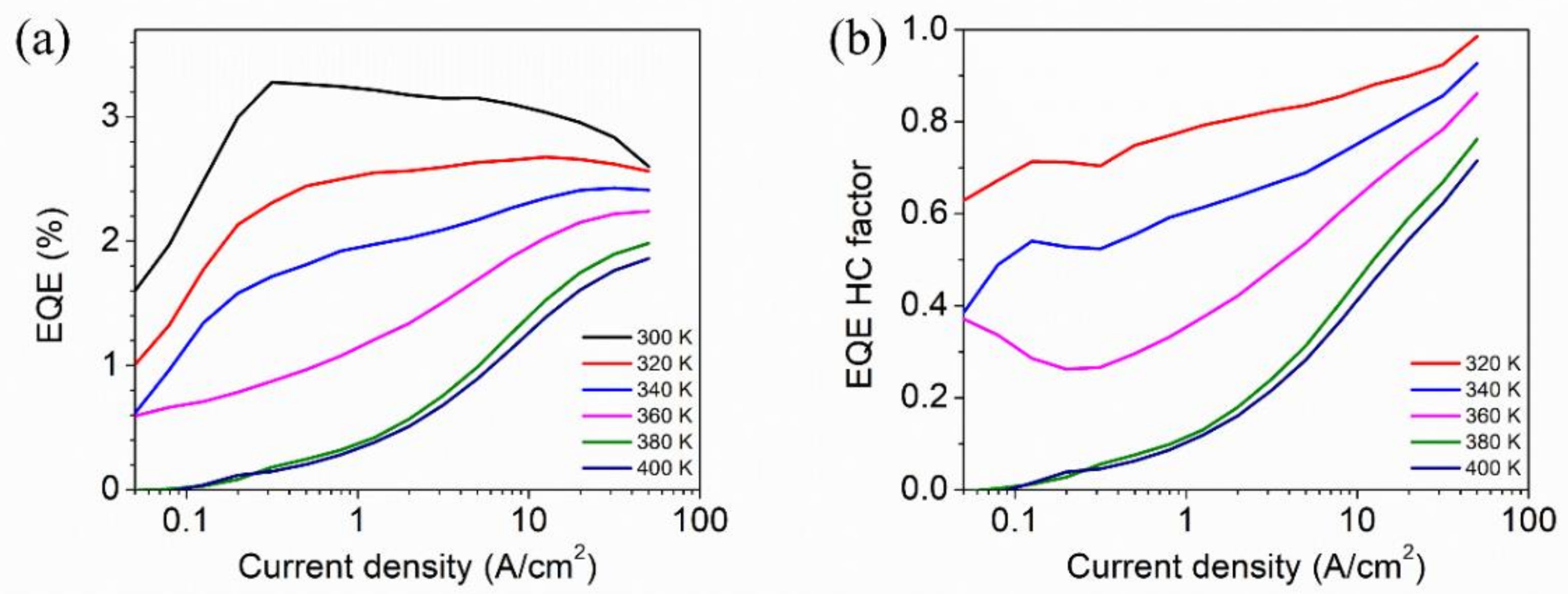
Figure 3.
(a) EL properties of red LEDs. (b) Output power-current-forward voltage and EQE vs. current. Copyright 2009 The Japan Society of Applied Physics [8].
Figure 3.
(a) EL properties of red LEDs. (b) Output power-current-forward voltage and EQE vs. current. Copyright 2009 The Japan Society of Applied Physics [8].

Figure 4.
(a) SEM image and (b) microscope EL image of 5 × 5 µm2 µLED; (c) EQE curves. These figures are reproduced from [5], with the permission of AIP Publishing.
Figure 4.
(a) SEM image and (b) microscope EL image of 5 × 5 µm2 µLED; (c) EQE curves. These figures are reproduced from [5], with the permission of AIP Publishing.

Figure 5.
PL wavelength comparison of MQWs grown on InGaNOS and GaN template. The figure is reproduced from [16], with the permission of AIP Publishing.
Figure 5.
PL wavelength comparison of MQWs grown on InGaNOS and GaN template. The figure is reproduced from [16], with the permission of AIP Publishing.
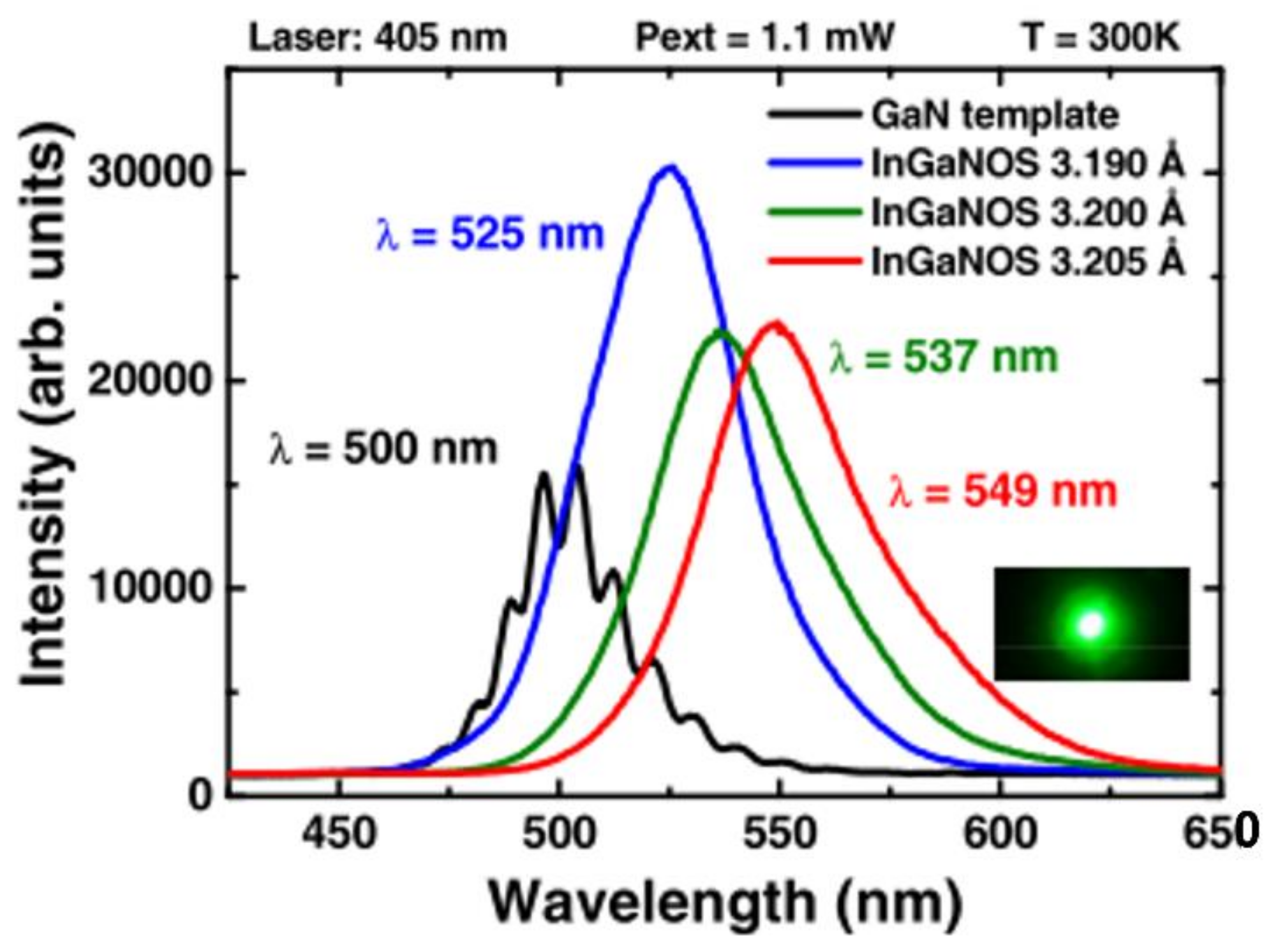
Figure 6.
(a) Scanning electron microscope of the red μLED with porous GaN; (b) XRD RSM; (c) peak wavelength and FWHM vs. J. Copyright 2009 The Japan Society of Applied Physics [20].
Figure 6.
(a) Scanning electron microscope of the red μLED with porous GaN; (b) XRD RSM; (c) peak wavelength and FWHM vs. J. Copyright 2009 The Japan Society of Applied Physics [20].

Figure 7.
(a) RSM and (b) AFM of as-grown epitaxy. (c) TEM of the DL after high-temperature GaN growth; (d) comparison of PL emission from MQWs regrown on GaN template and relaxed InGaN buffer. These figures are reproduced from [22], with the permission of AIP Publishing.
Figure 7.
(a) RSM and (b) AFM of as-grown epitaxy. (c) TEM of the DL after high-temperature GaN growth; (d) comparison of PL emission from MQWs regrown on GaN template and relaxed InGaN buffer. These figures are reproduced from [22], with the permission of AIP Publishing.
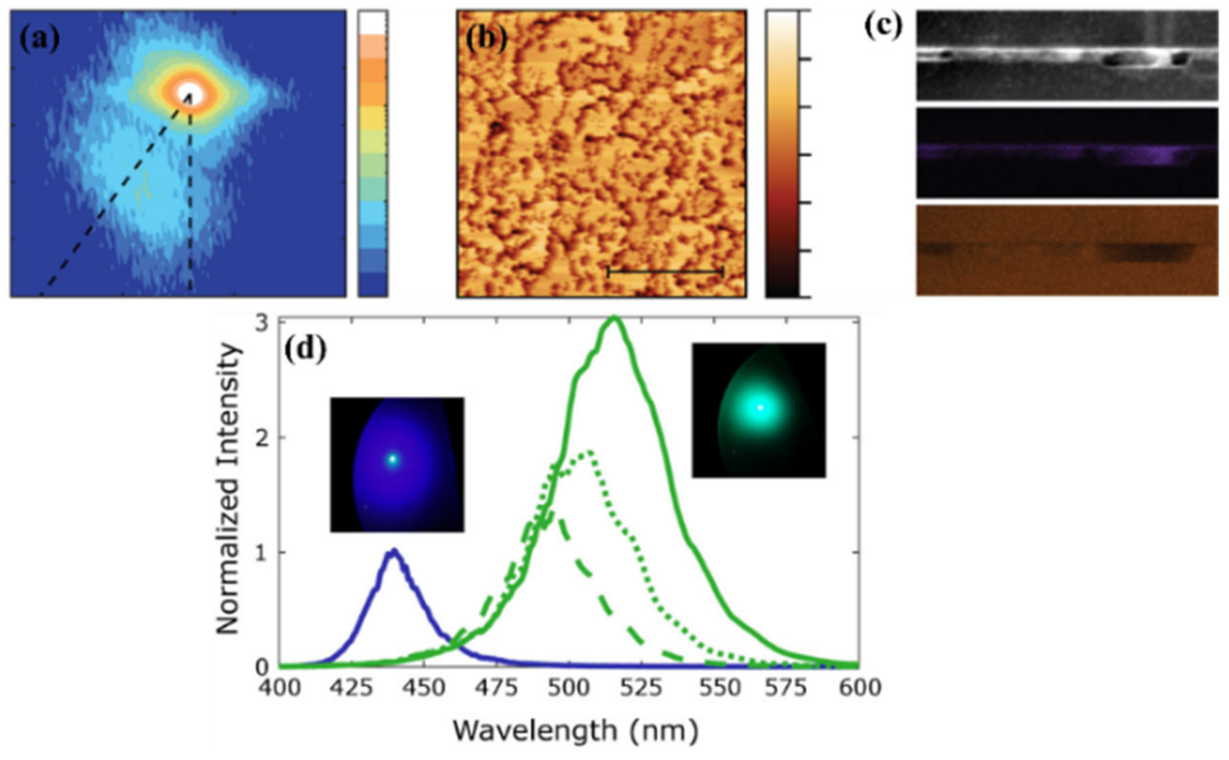
Figure 8.
(a) Cross-sectional epilayer design; (b) voltage and power measured from backside vs. J; (c) backside emission EQE as a function of J. Copyright 2009 The Japan Society of Applied Physics [21].
Figure 8.
(a) Cross-sectional epilayer design; (b) voltage and power measured from backside vs. J; (c) backside emission EQE as a function of J. Copyright 2009 The Japan Society of Applied Physics [21].

Publisher’s Note: MDPI stays neutral with regard to jurisdictional claims in published maps and institutional affiliations. |
© 2022 by the authors. Licensee MDPI, Basel, Switzerland. This article is an open access article distributed under the terms and conditions of the Creative Commons Attribution (CC BY) license (https://creativecommons.org/licenses/by/4.0/).
Share and Cite
MDPI and ACS Style
Li, P.; Li, H.; Wong, M.S.; Chan, P.; Yang, Y.; Zhang, H.; Iza, M.; Speck, J.S.; Nakamura, S.; Denbaars, S.P. Progress of InGaN-Based Red Micro-Light Emitting Diodes. Crystals 2022, 12, 541. https://doi.org/10.3390/cryst12040541
AMA Style
Li P, Li H, Wong MS, Chan P, Yang Y, Zhang H, Iza M, Speck JS, Nakamura S, Denbaars SP. Progress of InGaN-Based Red Micro-Light Emitting Diodes. Crystals. 2022; 12(4):541. https://doi.org/10.3390/cryst12040541
Chicago/Turabian StyleLi, Panpan, Hongjian Li, Matthew S. Wong, Philip Chan, Yunxuan Yang, Haojun Zhang, Mike Iza, James S. Speck, Shuji Nakamura, and Steven P. Denbaars. 2022. "Progress of InGaN-Based Red Micro-Light Emitting Diodes" Crystals 12, no. 4: 541. https://doi.org/10.3390/cryst12040541
Note that from the first issue of 2016, this journal uses article numbers instead of page numbers. See further details here.