
Defect-Free Phononic Crystal Waveguides on GaAs


Department of Physics, Engineering Physics & Astronomy, Queen’s University, Kingston, ON K7L 3N6, Canada
*
Author to whom correspondence should be addressed.
Crystals 2023, 13(11), 1540; https://doi.org/10.3390/cryst13111540
Submission received: 29 September 2023
/
Revised: 21 October 2023
/
Accepted: 24 October 2023
/
Published: 27 October 2023
(This article belongs to the Special Issue Advances in Phononic Crystals and Elastic Metamaterials)
Abstract
:A phononic crystal waveguide is presented that consists of the inverse of a typical structure. Instead of a defect waveguide within an extended phononic crystal, this waveguide consists of a phononic crystal of finite width, and the phononic crystal itself is composed of a shallow array of holes. The acoustic velocity is actually reduced in the phononic crystal region, which subsequently enables the waveguiding of the acoustic wave underneath the micro-structured surface. As the width of the waveguide increases with the number of inclusions, the waveguide morphs from an unstructured surface to an extended phononic crystal with a transitional modal region of an intermediate number of inclusions that is suitable for waveguiding. For the chosen phononic crystal parameters in terms of the hole depth and filling fraction, the optimum waveguide width of four inclusions is determined.
1. Introduction
The use of waveguides to control wave energy is now ubiquitous across many different types of wave systems. Waveguides for radio-frequency (RF) electromagnetic radiation are typically visualized as rectangular tubes, but the miniaturization of RF electronics has provided well-designed transmission lines on the micron scale [1]. In optics, ridge waveguides are materials with slower optical velocities surrounded by air or cladding with higher velocities that limit coupling to the outer environment and maintain the one-dimensional flow of wave energy [2]. With the advent of photonic crystal structures, the cladding is replaced by a photonic crystal, offering a valuable platform on which to develop a wide range of novel photonic crystal waveguide structures leading to optical circuits [3].
Similar to these other forms of wave energy, acoustics also has a compelling need for waveguide structures. While historic waveguides include medical and musical instruments, the broad use of surface acoustic wave (SAW) devices [4] naturally leads to the desire to better control and more efficiently transport this acoustic energy along well-defined channels and potential SAW-based acoustic circuits. Early conceptualizations of the slow layer for acoustic waveguiding have been discussed for thin films and homogeneous waveguide cores with cladding [5,6], while also expanding the discussion towards contiguous ridge and topographic waveguides, composite half-space waveguides and beam waveguides [6,7]. The concept of a "slow" and "fast" material has been described for such waveguides, indicating that mechanically soft and stiff materials (associated with slow and fast phase velocities, respectively) are necessary for good waveguiding. Typically, the fast material (or air) would be best suited for the cladding, and the slow material could then be used as the waveguide core. As an alternative to topographic waveguides, a waveguide on a planar substrate can be created by modifying the material properties near the surface by, for instance, using ion implantation [8,9]. In such an implementation, the altered regions become the slow waveguide layer with the original substrate becoming the cladding, or vice versa.
In an extension of the ridge waveguide structure, a one-dimensional array of blocks placed on a semi-infinite substrate has been shown to support the propagation of Rayleigh–Bloch waves [10]. This manner of waveguiding, using a phononic crystal (PnC) consisting of a one-dimensional periodic structure, provides the localization of Rayleigh waves laterally by slowing the phase velocity underneath the pillars. More recently, a periodic array of cylindrical pillars on a surface has also been shown to guide surface elastic waves via mode coupling of the pillars [11]. In addition to ridge waveguide and waveguide-like structures, PnC waveguide geometries are possible that mimic the waveguides in photonic crystals. Typical phononic waveguides therefore consider a PnC composed of holes in a material with a linear defect consisting of a row of missing holes [12,13,14,15,16]. As with photonic crystals, the waveguiding is enabled when the waveguide mode exists at a frequency inside the PnC bandgap, thus limiting motion to the direction of the waveguide.
In an alternative approach, we present here a composite model for a defect-free method of a PnC waveguide based on surface inclusions. The waveguide consists of a square phononic crystal array of finite width, where the shallow, cylindrical inclusions are a fraction of the acoustic wavelength (see Figure 1). An a priori understanding would suggest that removing mass from the surface, and lowering its average density, would not result in a "slow" layer compared to the pristine surface. However, the stiffness of the metamaterial-like surface is also altered such that the PnC of cylindrical void inclusions in GaAs indeed creates a slow layer. This concept can be seen in the phase velocity of the Rayleigh SAW modes in a shallow hole PnC compared to that of the GaAs surface [17]. For the shallow hole PnC on GaAs, the slow layer can be better suited as the waveguide core instead of a linear defect-based waveguide core, specifically regarding waveguides of the core cladding type.
2. Materials and Methods
The waveguide structure was modelled using the finite element method (FEM) in a fully three-dimensional geometry using eigenfrequency analysis in COMSOL Multiphysics, version 5 [18], along with the Structural Mechanics Module and the MEMS module to include piezoelectric effects. (See Section S1 of Supplemental Information.) The computational domain of the model consisted of a homogeneous half-space of -cut GaAs that was truncated to a depth of 50 μm and a length of 4 μm along the wave propagation direction. The width of the domain varied from 60 μm to 104 μm depending on the simulation performed, as discussed below. The cylindrical inclusions forming the PnC had a surface filling fraction of 0.564 and uniform array depths of 3 μm. The PnC was composed of a square lattice, with a lattice parameter of μm, with oriented along the -direction. The -direction of this GaAs surface is significant as it possesses the ability to support Rayleigh waves as well as being piezoelectric to enable the electrical generation of SAWs. The PnC geometry parallels earlier work, where the 3 μm depth of the inclusions was shown to allow them to act as a slow metamaterial with a significant difference in phase velocity compared to the substrate [17]. For visual reference, Figure 1 depicts a computational geometry with the exterior mesh visible and showing a waveguide core that is four inclusions wide along with 40 μm of cladding on either side; the maximum mesh element size is with the minimum size being .
In the computational volume, the values presented in Table 1 for the elastic stiffness constants and density are those used previously for GaAs by Tanaka and Tamura [19], and the piezoelectric properties are from COMSOL’s built-in Material Library. The surface boundary, including the surface of the cylindrical voids, was specified as a free boundary in COMSOL; hence, it was tractionless for the GaAs void to air interface. The bottom μm boundary was specified as a low-reflecting boundary [20], which was intended to perfectly match the mechanical impedance of pressure and shear waves from the medium. For the Bloch–Floquet boundary conditions, the μm extents (along the wave propagation direction) had a reduced wavevector of applied, giving a wavelength of 16 μm for the fundamental Rayleigh wave, which was four times larger than the lattice parameter of the PnC. Here, k is the wavevector magnitude in the -direction and is the wavevector magnitude at the -point of the Brillouin zone. Such a long wavelength was previously considered in the band structures of similar PnCs [17]. Being in the lowest frequency mode in the middle of the Brillouin zone (for an infinitely large periodic array of this type), this Rayleigh mode exhibits nearly linear dispersion and is far from higher-order modes or effects near the zone boundary. As a result, the mode with its long wavelength, as it is used here, will experience a homogenized, metamaterial-like waveguide behavior. This would suggest that the minimum finite length of a potential waveguide should be comparable to the acoustic wavelength as a full wave would then be impacted by the altered properties within the waveguide.
Many different solutions to the computational volume are provided by the solver, and, as a result, a variety of different criteria have been applied to distinguish modes of importance for this study. In particular, it is desirable to identify modes that reflect the properties of a SAW on a free GaAs surface. As with a SAW, the modes should reside near the surface. A surface strain energy ratio is therefore defined by , with the integrated strain energy contained in a volume near the surface of the computational domain (the upper 25 μm) or the entire computational domain for or , respectively. Only modes with a surface strain energy ratio greater than 0.6 are considered. The integrated strain energy in a target volume is determined by the relation
where is the stiffness tensor, is the strain tensor and the integral is performed over the target volume. In addition, it is desired that the modes are polarized similarly to the sagittally polarized Rayleigh modes in GaAs. The modes will then be characterized by a squared polarization ratio defined by
where , and are components of the displacement field, which are integrated over the entire computational domain [17,21,22]. A purely sagittal mode would therefore have . To consider a broad array of possible modes while maintaining sagittal polarization, only modes with a squared polarization ratio greater than 0.6 are considered.
To quantify a mode’s confinement within the waveguide, we also define the waveguide’s core strain energy ratio as , where is the integrated strain energy contained in the lateral region defined by the inclusion unit cells (Figure 1) and extending from the surface to the bottom of the domain. A core strain energy ratio of 0.5 would indicate that half of the waveguide mode is within the PnC core of the waveguide. To ensure that a significant fraction of the wave energy is contained within the PnC waveguide, a mode is defined as a core waveguide mode only if its core strain energy ratio is greater than 0.6 and in addition to the surface strain energy and the polarization criteria above.
3. Results
With the simulation geometry outlined above, an eigenfrequency analysis of a linear elastic and anisotropic GaAs material was conducted using COMSOL for PnCs of varying widths as defined by the number of inclusions. While the core widths of the waveguides were varied from a single row through 12 inclusions wide, the waveguide cladding was maintained at 28 μm on either side, or seven lattice parameters wide. In addition, these simulation models applied periodic boundary conditions to the lateral y-extents. Periodic boundary conditions result in an infinite number of adjacent waveguides, largely decoupled from each other but without the edge effects experienced with absorbing boundary conditions [23].
The real parts of the eigenfrequencies are plotted in Figure 2 for those modes with frequencies below 225 MHz. In addition, only those modes are plotted that meet the polarization and surface boundedness conditions. To help identify modes with the least attenuation of their acoustic power, the points in Figure 2 are color-coded according to their logarithmic reciprocal attenuation given by [17,24]. The reciprocal attenuation values provide a measure of the leakage of the acoustic energy into the bulk and away from the waveguide. The most resilient modes will therefore have larger reciprocal attenuation (less actual attenuation) and should be the focus of study. From Figure 2a, the higher-frequency modes are, generally, strongly attenuated.
The frequency of the Rayleigh mode on a free GaAs surface (177.99 MHz) is given by the red line in Figure 2. Given that waveguide frequencies less than that of the free GaAs are targeted for waveguiding, the higher frequencies can be ignored, with the lower-frequency modes of most interest. For reference, the displacement field map for the lowest-frequency mode at each width of inclusion is provided in Section S3 of the Supplementary Materials. Figure 2a also shows the frequency of the Rayleigh mode (171.10 MHz) on a surface with infinite inclusions of the same type as the waveguide [17]. With this, the lowest-frequency modes can typically be identified as the Rayleigh mode, as its frequency undergoes a transition from a GaAs surface-like mode for the narrowest waveguides to a PnC-like mode for a waveguide of 10 inclusions wide (or the SAW wavelength). This frequency transition follows a sigmoidal curve, and the frequencies for PnC widths from three to seven unit cells suggest that the mode is mixed between the PnC and unaltered surfaces.
To distinguish waveguide modes that are well contained by the PnC core, we used the waveguide’s core strain energy ratio provided above as a waveguide boundedness parameter. This criterion was applied to all modes in Figure 2a; the result after the removal process is shown in Figure 2b. Interestingly, all modes except the Rayleigh modes were removed from the plot. Further, the thinnest PnC core widths also disappeared as the velocity differential was not sufficiently slow to confine the modes to the waveguide—they remained more GaAs-substrate-like SAW modes. The introduction of this waveguide boundedness parameter therefore reveals modes with the majority of their energy bound within the PnC waveguide.
The widest PnC waveguide to pass the boundedness criterion (10 inclusions) is the slowest layer in contrast to the GaAs surface, as may be expected. The fact that this waveguide fulfilled the core strain energy ratio criterion may also be a result of it having a larger physical waveguide-to-domain ratio. Note, however, that the modes in these wider waveguide domains experience significantly higher attenuation. In contrast, the more confined modes in the narrower waveguides have a marked reduction in attenuation. This phenomenon seems to demonstrate that the tighter confinement and coupling to the Rayleigh modes in the waveguide cladding provide an improvement in the SAW attenuation for the narrower PnC core waveguides.
From Figure 2, a PnC geometry of four inclusions wide would therefore offer the most promising waveguiding behavior to channel SAWs. It would enable the best localization of a SAW due to its smaller lateral width, while also demonstrating that it can confine the acoustic energy sufficiently within the waveguide. In addition, the mode for the four-inclusion waveguide possesses the lowest attenuation of any mode, satisfying the localization condition imposed by the core strain energy ratio.
To model the four-inclusion waveguide, piezoelectric effects were added to the solid mechanics physics. The electrostatics in this model included piezoelectric charge conservation for the interior of the domain, Bloch-periodic conditions for the longitudinal boundaries ( μm) and a zero charge condition for all other domain boundaries. The computational domain was also increased to provide 40 μm (10 unit cells) of cladding on either side of the waveguide, giving a total width of 96 μm. In addition, the simulation model had low-reflecting boundary conditions applied to the y-extents (the planes μm in Figure 1) instead of periodic boundary conditions. Although the use of periodic boundary conditions has merit in this application, it was important to determine wave dissipation via bulk waves for this waveguide; thus, low-reflecting boundaries were chosen.
The eigenmode of the four-inclusion waveguide is a Rayleigh wave-like mode with an eigenfrequency of MHz. This yields a phase velocity of approximately 2810 m/s, which is 40 m/s less than the free semi-infinite GaAs substrate phase velocity, but 70 m/s faster than the infinite PnC [17]. The reciprocal attenuation was calculated to be , which is higher than the attenuation value of for the infinite two-dimensional array PnC equivalent [17], which will be discussed below. Figure 3 plots the magnitude of the (real) displacement field for the eigenmode of the waveguide. As expected, the displacement of the wave motion is well concentrated within the PnC core region and near the surface.
4. Discussion
To examine the waveguide mode more closely, the components of the real displacements , and are shown in Figure 4. The sagittal displacement components in the -plane are well confined to the waveguide, which is expected given the requirements of the polarization and core strain energy ratios. In contrast, the y-components of the displacement are much less localized. This may be due to the sagittal wave scattering from the inclusions and escaping laterally from the waveguide; however, there is no similarly strong z-component in the cladding, which indicates that this is not a simple scattered Rayleigh wave. This extended mode is therefore a delocalized shear component of the mode. The interesting, anti-symmetric nature of the surface features along with the reversal of the displacement below the inclusions further indicate that this shear component is not a simple energy-scattering mechanism. The complete waveguide mode therefore resembles a hybridization of the Rayleigh mode confined to the waveguide and this shear mode extending into the cladding. The y-displacement component seems to be accommodating strain from the sagittal waveguide mode. For the given phase of the waveguide mode propagation in Figure 4, the z-displacement is into the bulk, and both the x- and y-displacements are compressing the inclusions at the surface in a type of breathing mode. For the material below the inclusions, the negative z-displacement compresses the bulk with the strain being accommodated by lateral shear outwards from the waveguide. While the non-local extent of reaches towards the lateral absorbing boundaries and this could also contribute to the attenuation for this waveguide mode, a different aspect of this lateral shear component is found to be the dominant source of loss in the waveguide. In a previous work [17], the Rayleigh mode of an infinite PnC had a velocity below that of the longitudinal and shear vertical modes (as expected), but the Rayleigh mode was supersonic relative to the shear horizontal mode. As a result, the lateral shear component could couple to bulk modes and radiate energy into the bulk. This can be seen in the animation included with the Supplementary Materials, which shows acoustic energy radiating into the bulk with a lateral extent beyond the waveguide. Even with the lateral shear component, the mode of the four-inclusion waveguide can still be considered as a primarily localized SAW mode, with predominantly Rayleigh wave-like behavior. The displacement component, while extending beyond the waveguide, is much weaker than the sagittal displacement components, and, as shown in Figure 3, the total displacement is dominated by contributions within the PnC waveguide.
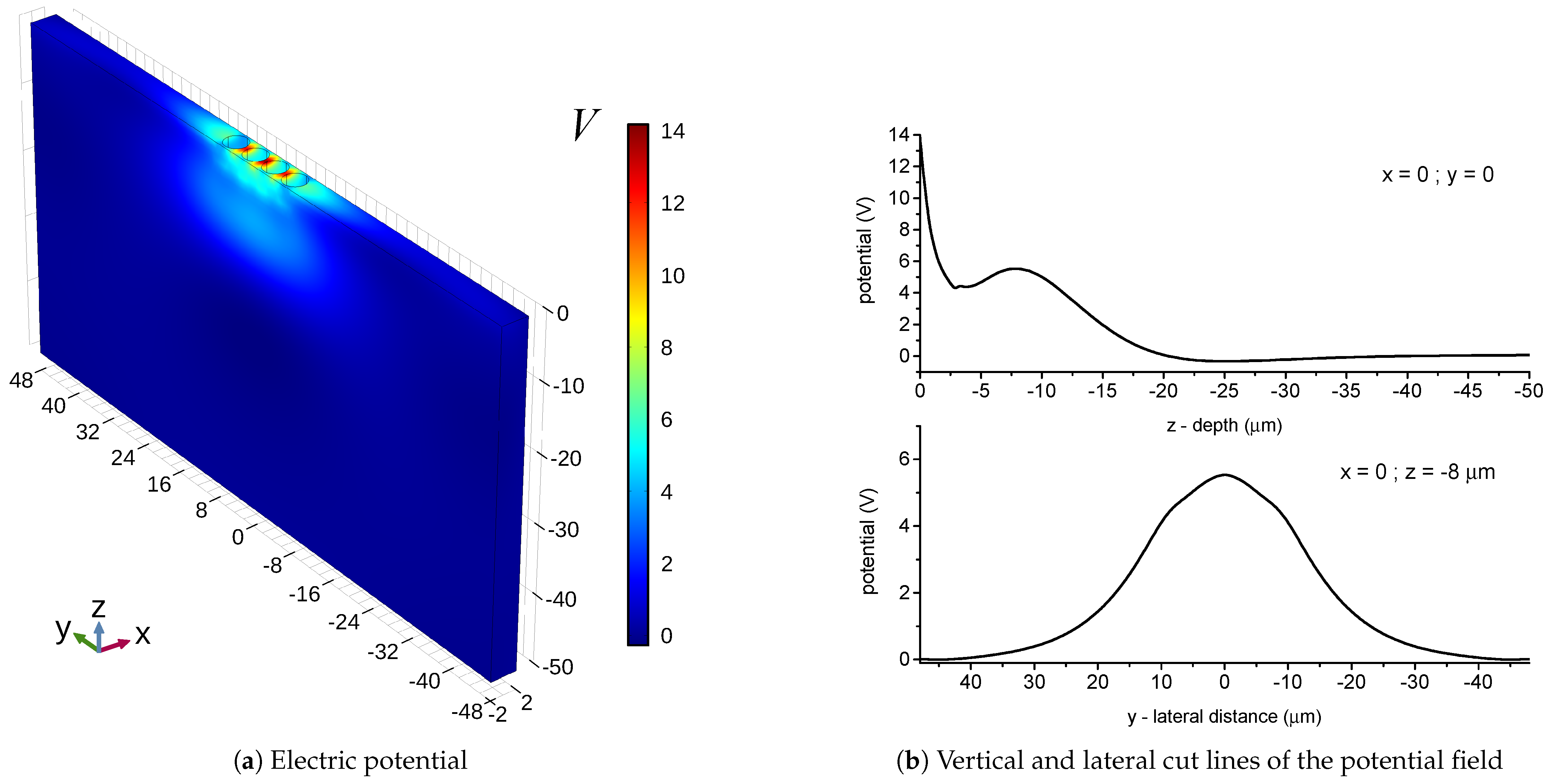
Given the ability of this PnC waveguide to guide acoustic waves, one interesting application of it would extend to previous work using SAWs to transport charge and spin in GaAs nanostructures for quantum information processing. In previous attempts to better control carriers, a variety of different configurations have been used to create lateral control, such as electrostatic gates [25], quantum wires [26] and dynamic quantum dots [27]. More recent work has shown that moving, piezoelectrically defined dots can not only coherently transport spin carriers, but that the strain of the acoustic waves can also modulate spin information within the coherence length of transport [28]. Moving forward, more complicated paths with good carrier localization could be used to extend the ideas in these earlier works and potentially provide a platform for acoustically enabled circuitry. SAW waveguides are one implementation that could allow the flexibility for varied, acoustically enabled charge and spin transport paths as long as the piezoelectric performance can mimic the lateral confinement of the strain waves. With these exciting possibilities in mind, the piezoelectric potential generated by the four-inclusion waveguide in GaAs studied above is plotted in Figure 5. The potential is very strong near the surface, coinciding with the large displacements in the PnC waveguide core. However, there is also a local maximum in both the depth and width underneath the inclusions that could be coupled to quantum nanostructures. Given the linearity of the elastic system, the excitation frequencies and PnC waveguide geometries could be scaled to reduce the spatial dimensions needed to preserve spin coherence [29]. Such potential dots could then provide the lateral confinement of electron spins needed to support long-range spin transport and enable more complex geometries for the implementation of dynamic quantum dots.
5. Conclusions
We have shown that well-localized wave motion can be achieved using a PnC waveguide of finite width. The PnC acts as the waveguide core and allows the wave to propagate since the wavevector (with a wavelength longer than multiple unit cells) is chosen to be far from the Brillouin zone edges where Bragg diffraction occurs. For a waveguide of four inclusions wide, the SAW propagates along the metamaterial-like core, with the majority of its energy in or near the waveguide core. The confinement of the Rayleigh modes within the metamaterial PnC core is quite different than the resonating pillar modes that have been previously reported [11]. In addition to the primary sagittal wave motion, there is a small but important shear () component of the waveguide mode, which seems to accommodate the strain localized in the waveguide but is also a source of loss. This presentation of a guided mode in the inverted phononic crystal surveys a small fraction of the parameter space for this type of device. Consequently, there are numerous possibilities for potential improvements to the design to minimize the shear component to the mode. Further exploration of the metamaterial-like nature of the waveguide could present a single material platform to study other interesting physical phenomena that may occur within the Brillouin zone, such as Dirac-like cone dispersion [30] or backward propagating waves [31].
It is also noted that the piezoelectric potential generated by the waveguide mode is localized below the waveguide inclusions and, given that piezoelectrically defined potentials have provided some of the longest spin coherence lengths in GaAs, the PnC waveguide is a potential candidate for the creation of lateral confinement for acoustically enabled spin transport and control [28]. Future iterations of the waveguide design with varied inclusion profiles could enable non-trivial structures and optimize acoustic confinement. Further, the relatively minimal surface processing for this defect-free PnC waveguide could be advantageous if used as a platform for acoustic circuits and potential acoustically enabled circuits for quantum information processing.
Supplementary Materials
The following supporting information can be downloaded at: https://www.mdpi.com/article/10.3390/cryst13111540/s1, Section S1: Materials and Methods: Additional Information; Section S2: Additional Simulation Parameters; Section S3: Additional Simulation Results; Video S1: Time dependence of the total displacement field for the 10-inclusion waveguide showing coupling to bulk modes (171.29 MHz).
Author Contributions
Conceptualization, E.M. and J.A.H.S.; methodology, E.M.; formal analysis, E.M.; writing—original draft preparation, E.M.; writing—review and editing, E.M. and J.A.H.S.; visualization, E.M. and J.A.H.S.; supervision, J.A.H.S.; funding acquisition, J.A.H.S. All authors have read and agreed to the published version of the manuscript.
Funding
This research was funded by the Natural Science and Engineering Research Council of Canada under Discovery Grant RGPIN/05701-2014. The authors would also like to gratefully recognize CMC Microsystems for the provision of products and services that facilitated this research, including Design Tools and computational resources.
Data Availability Statement
Data are presented within the article and Supplementary Materials.
Acknowledgments
The authors would like to gratefully acknowledge the open source GNU Octave project, whose software was used to generate the plots in this work [32].
Conflicts of Interest
The authors declare no conflict of interest.
Abbreviations
The following abbreviations are used in this manuscript:
| RF | Radio-frequency |
| SAW | Surface acoustic wave |
| PnC | Phononic crystal |
| FEM | Finite element method |
References
- Vecchi, F.; Repossi, M.; Eyssa, W.; Arcioni, P.; Svelto, F. Design of Low-Loss Transmission Lines in Scaled CMOS by Accurate Electromagnetic Simulations. IEEE J. Solid-State Circuits 2009, 44, 2605–2615. [Google Scholar] [CrossRef]
- Webster, M.A.; Pafchek, R.M.; Sukumaran, G.; Koch, T.L. Low-loss quasi-planar ridge waveguides formed on thin silicon-on-insulator. Appl. Phys. Lett. 2005, 87, 231108. [Google Scholar] [CrossRef]
- Lin, S.Y.; Chow, E.; Hietala, V.; Villeneuve, P.R.; Joannopoulos, J.D. Experimental Demonstration of Guiding and Bending of Electromagnetic Waves in a Photonic Crystal. Science 1998, 282, 274–276. [Google Scholar] [CrossRef]
- Delsing, P.; Cleland, A.N.; Schuetz, M.J.A.; Knörzer, J.; Giedke, G.; Cirac, J.I.; Srinivasan, K.; Wu, M.; Balram, K.C.; Bäuerle, C.; et al. The 2019 surface acoustic waves roadmap. J. Phys. D Appl. Phys. 2019, 52, 353001. [Google Scholar] [CrossRef]
- Auld, B.A. Acoustic Fields and Waves in Solids, Vols. I and II; John Wiley & Sons, Inc.: New York, NY, USA, 1973. [Google Scholar]
- Ash, E.A.; De La Rue, R.M.; Humphryes, R.F. Microsound Surface Waveguides. IEEE Trans. Microw. Theory Tech. 1969, 17, 882–892. [Google Scholar] [CrossRef]
- Modica, G.; Zhu, R.; Horvath, R.; Beaudoin, G.; Sagnes, I.; Braive, R. Slow propagation of 2 GHz acoustical waves in a suspended GaAs phononic waveguide on insulator. Appl. Phys. Lett. 2020, 117, 193501. [Google Scholar] [CrossRef]
- Oliner, A.A. Waveguides for surface waves. In Acoustic Surface Waves; Springer: Berlin/Heidelberg, Germany, 1978; pp. 187–223. [Google Scholar] [CrossRef]
- Mei, J.; Friend, J. A review: Controlling the propagation of surface acoustic waves via waveguides for potential use in acoustofluidics. Mech. Eng. Rev. 2020, 7, 19-00402. [Google Scholar] [CrossRef]
- Porter, R.; Evans, D.V. Embedded Rayleigh–Bloch surface waves along periodic rectangular arrays. Wave Motion 2005, 43, 29–50. [Google Scholar] [CrossRef]
- Al Lethawe, M.; Addouche, M.; Benchabane, S.; Laude, V.; Khelif, A. Guidance of surface elastic waves along a linear chain of pillars. AIP Adv. 2016, 6, 121708. [Google Scholar] [CrossRef]
- Khelif, A.; Choujaa, A.; Benchabane, S.; Djafari-Rouhani, B.; Laude, V. Guiding and bending of acoustic waves in highly confined phononic crystal waveguides. Appl. Phys. Lett. 2004, 84, 4400–4402. [Google Scholar] [CrossRef]
- Olsson, R.H., III; El-Kady, I. Microfabricated phononic crystal devices and applications. Meas. Sci. Technol. 2009, 20, 012002. [Google Scholar] [CrossRef]
- Muzar, E.; Aval, G.A.; Stotz, J.A.H. Wet-etched phononic crystal waveguiding on GaAs. J. Phys. D Appl. Phys. 2018, 51, 044001. [Google Scholar] [CrossRef]
- Benchabane, S.; Gaiffe, O.; Salut, R.; Ulliac, G.; Laude, V.; Kokkonen, K. Guidance of surface waves in a micron-scale phononic crystal line-defect waveguide. Appl. Phys. Lett. 2015, 106, 081903. [Google Scholar] [CrossRef]
- Laude, V. Principles and properties of phononic crystal waveguides. APL Mater. 2021, 9, 080701. [Google Scholar] [CrossRef]
- Muzar, E.; Stotz, J.A.H. Surface acoustic wave modes in two-dimensional shallow void inclusion phononic crystals on GaAs. J. Appl. Phys. 2019, 126, 025104. [Google Scholar] [CrossRef]
- Eigenfrequency Analysis. 2018. Available online: https://www.comsol.com/multiphysics/eigenfrequency-analysis (accessed on 1 October 2023).
- Tanaka, Y.; Tamura, S. Surface acoustic waves in two-dimensional periodic elastic structures. Phys. Rev. B 1998, 58, 7958–7965. [Google Scholar] [CrossRef]
- COMSOL. Structural Mechanics Module User’s Guide: Version 5.3. 2017. Available online: https://doc.comsol.com/5.3/doc/com.comsol.help.sme/StructuralMechanicsModuleUsersGuide.pdf (accessed on 1 October 2023).
- Liu, T.W.; Tsai, Y.C.; Lin, Y.C.; Ono, T.; Tanaka, S.; Wu, T.T. Design and fabrication of a phononic-crystal-based Love wave resonator in GHz range. AIP Adv. 2014, 4, 124201. [Google Scholar] [CrossRef]
- Achaoui, Y.; Khelif, A.; Benchabane, S.; Laude, V. Polarization state and level repulsion in two-dimensional phononic crystals and waveguides in the presence of material anisotropy. J. Phys. D Appl. Phys. 2010, 43, 185401. [Google Scholar] [CrossRef]
- Laude, V. Phononic Crystals; De Gruyter: Berlin, Germany; Boston, MA, USA, 2015. [Google Scholar] [CrossRef]
- Maznev, A.A.; Every, A.G. Surface acoustic waves in a periodically patterned layered structure. J. Appl. Phys. 2009, 106, 113531. [Google Scholar] [CrossRef]
- Hermelin, S.; Takada, S.; Yamamoto, M.; Tarucha, S.; Wieck, A.D.; Saminadayar, L.; Bäuerle, C.; Meunier, T. Electrons surfing on a sound wave as a platform for quantum optics with flying electrons. Nature 2011, 477, 435–438. [Google Scholar] [CrossRef]
- Couto, O.D.D.; Lazić, S.; Iikawa, F.; Stotz, J.A.H.; Jahn, U.; Hey, R.; Santos, P.V. Photon anti-bunching in acoustically pumped quantum dots. Nat. Photonics 2009, 3, 645–648. [Google Scholar] [CrossRef]
- Stotz, J.A.H.; Hey, R.; Santos, P.V.; Ploog, K.H. Coherent spin transport through dynamic quantum dots. Nat. Mater. 2005, 4, 585–588. [Google Scholar] [CrossRef] [PubMed]
- Helgers, P.L.J.; Stotz, J.A.H.; Sanada, H.; Kunihashi, Y.; Biermann, K.; Santos, P.V. Flying electron spin control gates. Nat. Commun. 2022, 13, 5384. [Google Scholar] [CrossRef] [PubMed]
- Stotz, J.A.H.; Hey, R.; Santos, P.V.; Ploog, K.H. Enhanced spin coherence via mesoscopic confinement during acoustically induced transport. New J. Phys. 2008, 10, 093013. [Google Scholar] [CrossRef]
- Maznev, A.A. Dirac cone dispersion of acoustic waves in plates without phononic crystals. J. Acoust. Soc. Am. 2014, 135, 577–580. [Google Scholar] [CrossRef] [PubMed]
- Maznev, A.; Every, A. Existence of backward propagating acoustic waves in supported layers. Wave Motion 2011, 48, 401–407. [Google Scholar] [CrossRef]
- Eaton, J.W.; Bateman, D.; Hauberg, S.; Wehbring, R. GNU Octave Version 4.2.1 Manual: A High-Level Interactive Language for Numerical Computations. 2017. Available online: https://www.gnu.org/software/octave/doc/v4.2.1/ (accessed on 1 October 2023).
Figure 1.
Phononic crystal waveguide geometry. The full computational volume for a four-inclusion waveguide with 40 μm of cladding shows the exterior mesh (scale: microns). On the right is a unit cell of the phononic crystal consisting of a GaAs matrix with a shallow inclusion. For this work, μm, μm, μm and μm.

Figure 2.
Real frequencies of the modes for waveguides of various PnC widths. The lines depict the frequencies of the Rayleigh wave on a defect-free GaAs surface (177.99 MHz; red) and on a surface with infinite inclusions (171.10 MHz; blue). The color of the points corresponds to the logarithmic reciprocal attenuation. All eigenmodes below 225 MHz are displayed in (a), while only those with a core strain energy ratio greater than 0.6 are shown in (b).
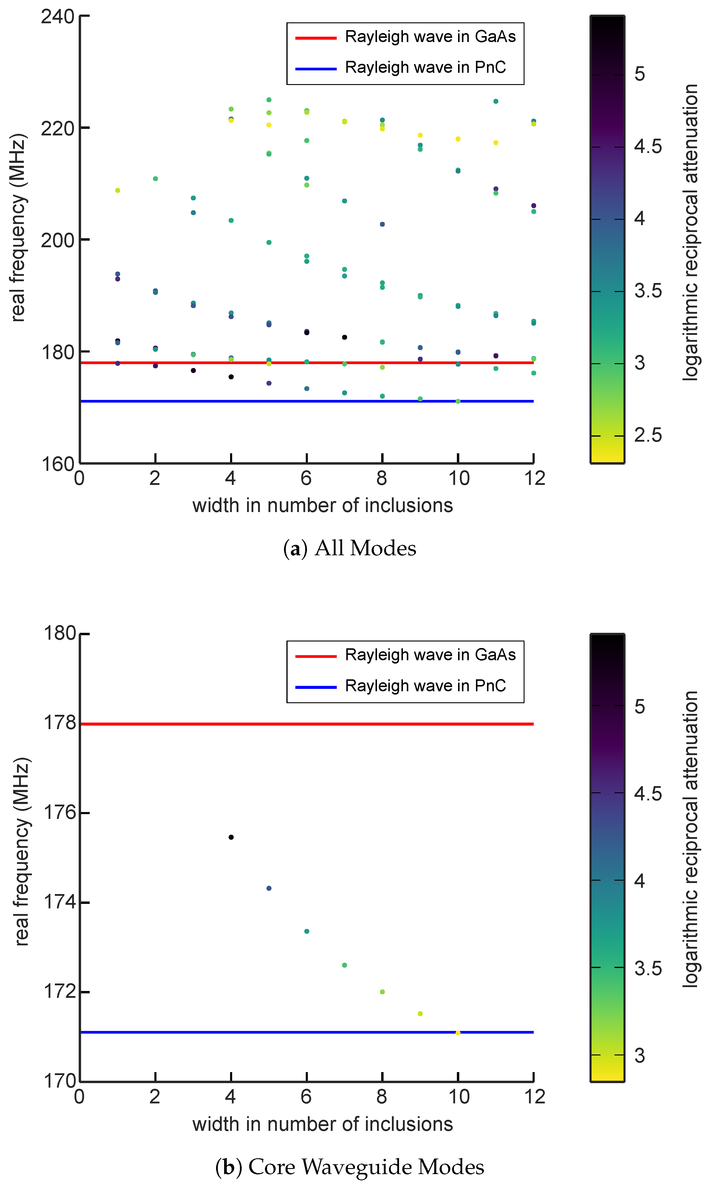
Figure 3.
The magnitude of the total displacement field from the mode for the four-inclusion waveguide consisting of 3 μm deep inclusions. Scale: microns.
Figure 3.
The magnitude of the total displacement field from the mode for the four-inclusion waveguide consisting of 3 μm deep inclusions. Scale: microns.
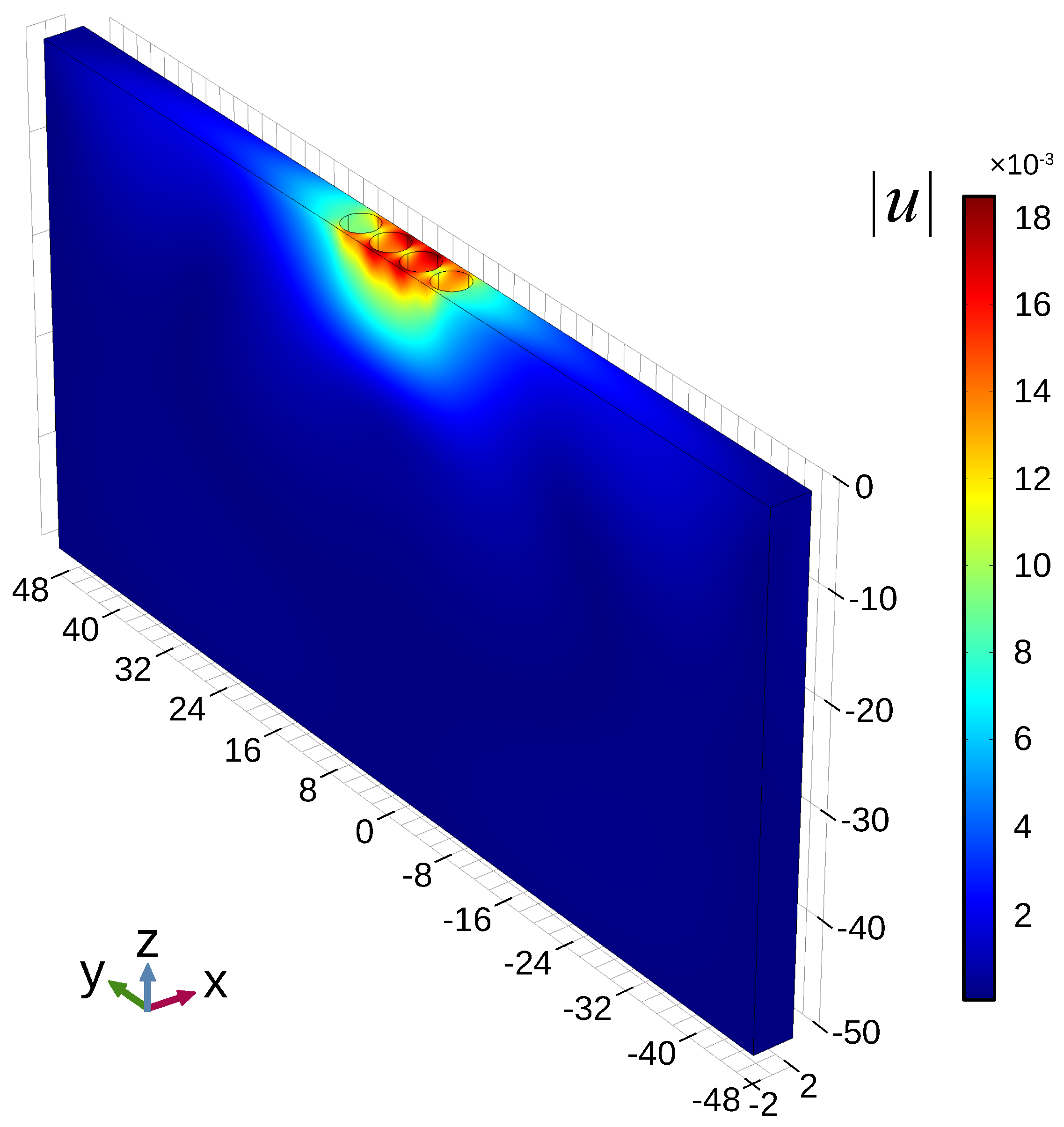
Figure 4.
Displacement fields for the four-inclusion waveguide mode consisting of 3 μm deep inclusions (175.40 MHz). The color scale shows the local displacement of the waveguide mode along the (a) x-, (b) y- and (c) z-directions. Scale: microns.
Figure 4.
Displacement fields for the four-inclusion waveguide mode consisting of 3 μm deep inclusions (175.40 MHz). The color scale shows the local displacement of the waveguide mode along the (a) x-, (b) y- and (c) z-directions. Scale: microns.
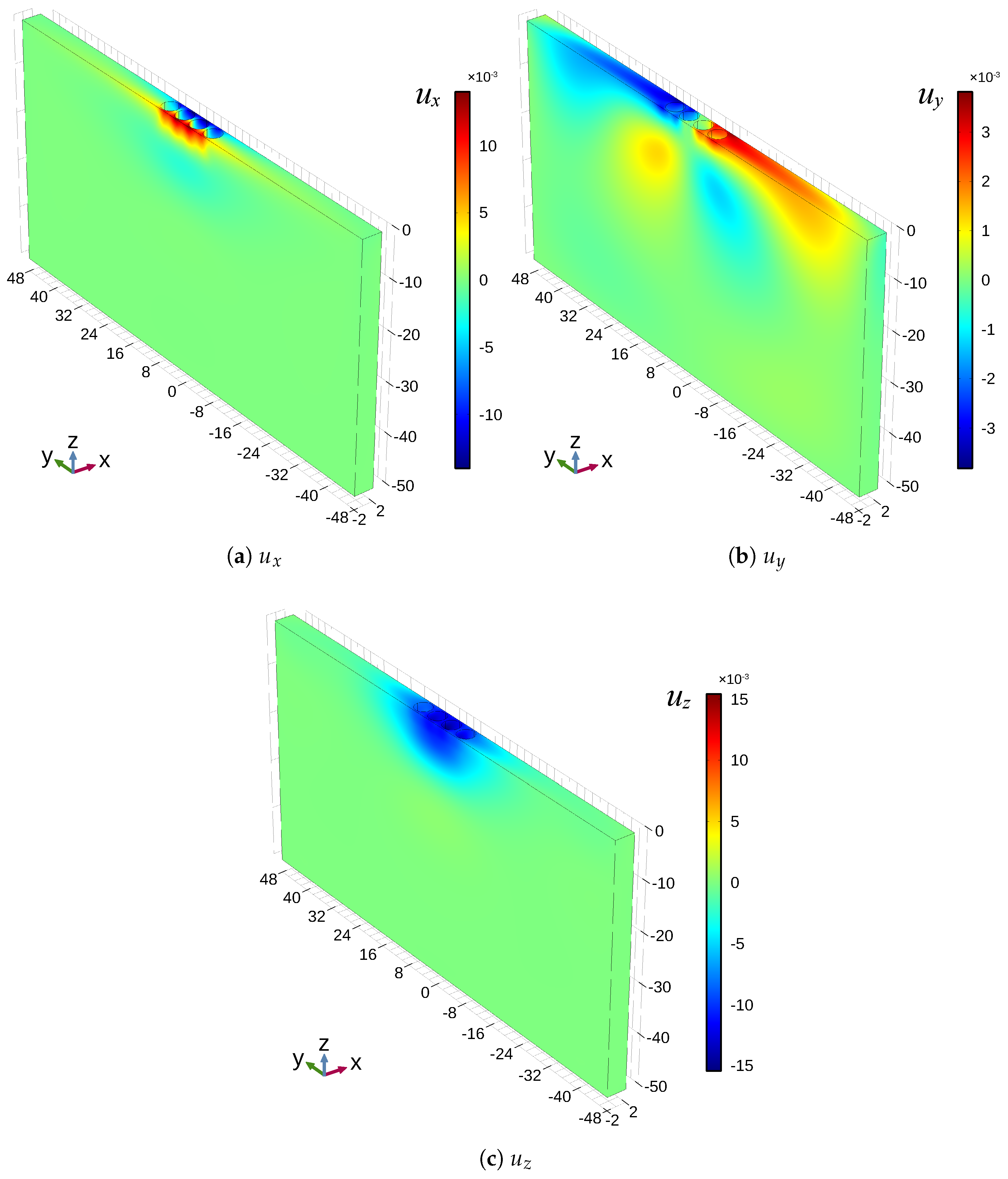
Figure 5.
Electric potential from the mode for the four-inclusion waveguide consisting of 3 μm deep inclusions (175.40 MHz). The 3D intensity map is provided in (a) and line plots along significant lines are shown in (b), where the upper panel shows the depth dependence of the potential in the middle of the computational domain and the lower panel provides the lateral dependence near the local maximum at μm. Scale: microns.

Table 1.
The values for GaAs material properties used in COMSOL for modelling. The mass density and elastic constants reflect those used previously by Tanaka and Tamura [19]. The piezoelectric coupling and relative permittivity parameters are from the built-in piezoelectric material constants in COMSOL.
| Constant | Value | Unit |
|---|---|---|
| 5360 | kg/m3 | |
| 11.88 | Pa | |
| = = | 5.38 | Pa |
| 5.94 | Pa | |
| 0.139785 | C/m2 | |
| 12.459 |
Disclaimer/Publisher’s Note: The statements, opinions and data contained in all publications are solely those of the individual author(s) and contributor(s) and not of MDPI and/or the editor(s). MDPI and/or the editor(s) disclaim responsibility for any injury to people or property resulting from any ideas, methods, instructions or products referred to in the content. |
© 2023 by the authors. Licensee MDPI, Basel, Switzerland. This article is an open access article distributed under the terms and conditions of the Creative Commons Attribution (CC BY) license (https://creativecommons.org/licenses/by/4.0/).
Share and Cite
MDPI and ACS Style
Muzar, E.; Stotz, J.A.H. Defect-Free Phononic Crystal Waveguides on GaAs. Crystals 2023, 13, 1540. https://doi.org/10.3390/cryst13111540
AMA Style
Muzar E, Stotz JAH. Defect-Free Phononic Crystal Waveguides on GaAs. Crystals. 2023; 13(11):1540. https://doi.org/10.3390/cryst13111540
Chicago/Turabian StyleMuzar, Edward, and James A. H. Stotz. 2023. "Defect-Free Phononic Crystal Waveguides on GaAs" Crystals 13, no. 11: 1540. https://doi.org/10.3390/cryst13111540
Note that from the first issue of 2016, this journal uses article numbers instead of page numbers. See further details here.