Article

Fabrication of SiC-on-Insulator (SiCOI) Layers by Chemical Vapor Deposition of 3C-SiC on Si-in-Insulator Substrates at Low Deposition Temperatures of 1120 °C

Crystal Growth Lab, Materials Department 6, University of Erlangen-Nürnberg, 91058 Erlangen, Germany
*
Author to whom correspondence should be addressed.
Crystals 2023, 13(11), 1590; https://doi.org/10.3390/cryst13111590
Submission received: 29 September 2023 / Revised: 10 November 2023 / Accepted: 15 November 2023 / Published: 17 November 2023
(This article belongs to the Special Issue Epitaxial Growth of Semiconductor Materials and Devices)

Abstract

:
Compared to bulk silicon carbide (SiC) wafers, SiC-on-insulator (SiCOI) substrates enable new device designs of electronic switches as well as novel photonic applications. One application is a micro-resonator for the usage in a Kerr frequency comb. For SiCOI substrates, a deposition temperature below 1200 °C is advisable due to stability reasons of the buried oxide layer during chemical vapor deposition (CVD) process conditions. To create 3C-SiC-on-insulator layers, a cold-wall CVD reactor was utilized, with propane and silane as the sources for carbon and silicon, respectively. To improve the cracking of the carbon source gas at low temperatures, the inner setup of the utilized cold-wall CVD reactor was changed to a non-water-cooled system. The change of the inner reactor setup was investigated numerically, and the grown epitaxial layers were characterized by Raman, EDX, SEM-imaging and XRD spectroscopy. We demonstrate successful deposition of 3C-SiC epitaxial layer substrates at temperatures below 1200 °C without delamination on SOI.

1. Introduction

Silicon carbide (SiC) has been established as a key wide bandgap semiconductor material in the area of high-power, high-temperature and optoelectronic applications. Due to its unique optical properties like a high third-order optical nonlinearity and a high refractive index, it is suitable to create photonic integrated circuits, such as a micro-resonator in a Kerr frequency comb [1,2]. To facilitate a light-guiding structure, photons can be confined in a layer made of a higher refractive index material surrounded by a lower refractive index material by total internal reflection. 3C-SiC exhibits a refractive index of 2.55. If enclosed by air and SiO2 with a refractive index of 1 and 1.45, respectively, it can act as a waveguide material [3,4].
Therefore, the fabrication of SiC-on-insulator (SiCOI) is of great interest. This has already been demonstrated, however, although at higher temperatures above 1200 °C [5]. In addition, an integration of such waveguide structures into the silicon MOS (metal oxide semiconductor) technology creates a new opto-micro-electronic device platform. Low process temperatures below 1200 °C are a prerequisite to retain CMOS compatibility and prevent diffusion of the buried SiO2 layer [6]. However, the cracking of the carbon species (i.e., propane) is diminished at lower temperatures. The utilized horizontal cold-wall CVD reactor AIX 200/4 SiC exhibits a water-cooled quartz susceptor holder, which carries the inductively heated graphite susceptor. The propane gas, as depicted in Figure 1, will not be heated up until it reaches the hot graphite plate, because the quartz susceptor holder will be kept at 20 °C during the process. In this work, we replaced the quartz susceptor holder with a ceramic based one, which is stable at temperatures up to 1600 °C and thus does not need to be water-cooled. Due to the lack of water cooling in the case of the ceramic holder, the propane gas will now be heated before reaching the susceptor and the substrate. This should improve the cracking of the propane gas flux. The impact of this change on the temperature field and temperature of the propane gas was investigated numerically utilizing the software COMSOL Multiphysics. 3C-SiC-on-Si samples were grown with both the quartz and the ceramic susceptor carrier. Subsequently, the epitaxial layer’s thickness was measured to quantify the amount of cracking of the carbon gas species. The epitaxial layers were further investigated with SEM imaging, EDX measurements, XRD measurements and Raman spectroscopy.

2. Material and Methods

For conducting the epitaxial growth of 3C-SiC, a horizontal cold-wall CVD reactor AIX 200/4 SiC setup was utilized. As precursor gases silane (10% SiH4/90% H2) and propane were used. Additional H2 functions as the carrier gas, purified to 6N. Using a high-frequency generator (Hüttinger TIG 20/300, Freiburg, Germany), the revolving graphite susceptor was inductively heated to temperatures of up to 1200 °C for the quartz susceptor carrier and 1120 °C for the ceramic susceptor carrier. The temperature was measured with the help of an optical differential pyrometer and a thermocouple built into the susceptor carrier. The employed SOI substrates with a resistivity of 1–20 Ω cm exhibit a 70 nm Si layer on top of a 2000 nm SiO2 layer. The underlying p-doped (boron) Si layer is oriented in the [100] direction. The Si substrates are an n-doped (phosphorus) [100] silicon wafer from SIEGERT WAFER GmbH with a resistivity of 10–20 Ω cm. A preceding cleaning step of the substrates was carried out, consisting of a 5 min ultrasonic bath at 70 °C in acetone, ethanol, H2O2/HCl and H2O2/NH3. Each epitaxy was performed according to the following steps, starting with a hydrogen cleaning step at 800 °C and 20 mbar of ambient pressure for 20 min, followed by a carbonization step at 800 °C and 150 mbar pressure for 10 min to convert the 70 nm Si layer into a SiC buffer layer, and a final growth step at temperatures of 1120 °C for the ceramic susceptor carrier, 1200 °C for the quartz susceptor carrier, and 150 mbar ambient pressure for 1 h. An overview of all grown epitaxial layers is given in Table 1.
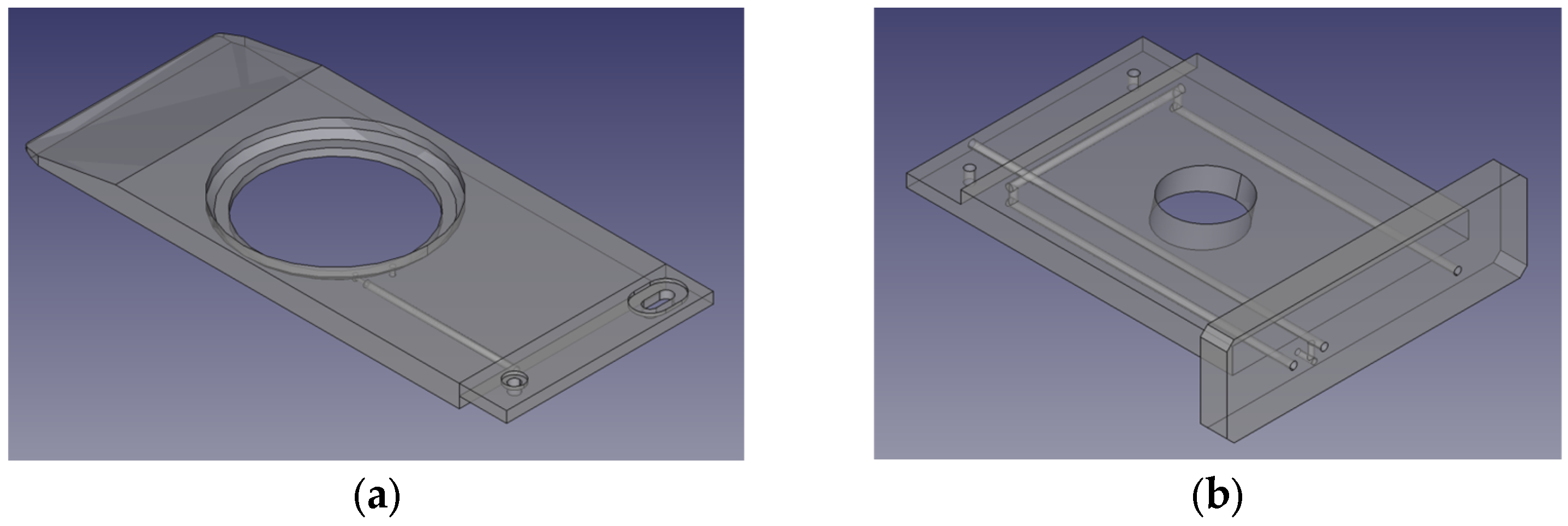
Since quartz glass exhibits a transformation temperature at around 1200 °C, it has to be cooled during normal epitaxy conditions. The standard susceptor carrier implemented in the AIX 200/4 setup is therefore water-cooled. While the low coefficient of thermal expansion allows high temperature gradients inside the quartz glass without breaking, it also means that the gas flow, as shown in Figure 1, will be kept at the corresponding temperature of the cooling water until it reaches the heated graphite susceptor. A new two-part susceptor carrier without water-cooling for the part closer to the magnetic field was designed. The utilized material for holding the inductively-heated graphite susceptor needs to be stable at high temperatures without water-cooling in a hydrogen-enriched atmosphere and non-inductive itself. High-purity Al2O3 ceramics fulfill these conditions. The part of the susceptor carrier further away of the magnetic field can be built using the hydrogen resistant 1.4006 steel alloy. Both parts are depicted in Figure 2.
The modeling of the gas flow and the temperature field of both the quartz- and ceramic susceptor holder has been carried out by utilizing the software COMSOL Multiphysics. The inner reactor setup was modeled in 3D and the temperature change of the propane gas flux investigated. Constant values of 20 °C for the cooling water and the inflowing gases and temperatures of 1120 °C and 1200 °C for the graphite susceptor were used for the modeling.
For the XRD measurements, a Panalytical Empyrean XRD setup (Malvern Panalytical GmbH, Kassel, Germany) was employed. For all measurements, the following parameters were set: 0.013° step-size, 50 s/step and 30 rpm sample rotation. A LabRAM HR Evolution Raman spectroscopy setup was employed, utilizing an 1800 gr/mm grating and a 532 nm laser. The EDX measurements were taken by a Jeol JSM-7610F Field emission scanning electron microscope (Jeol LTD, Akishima, Tokyo, Japan).

3. Results

3.1. Numerical Simulation

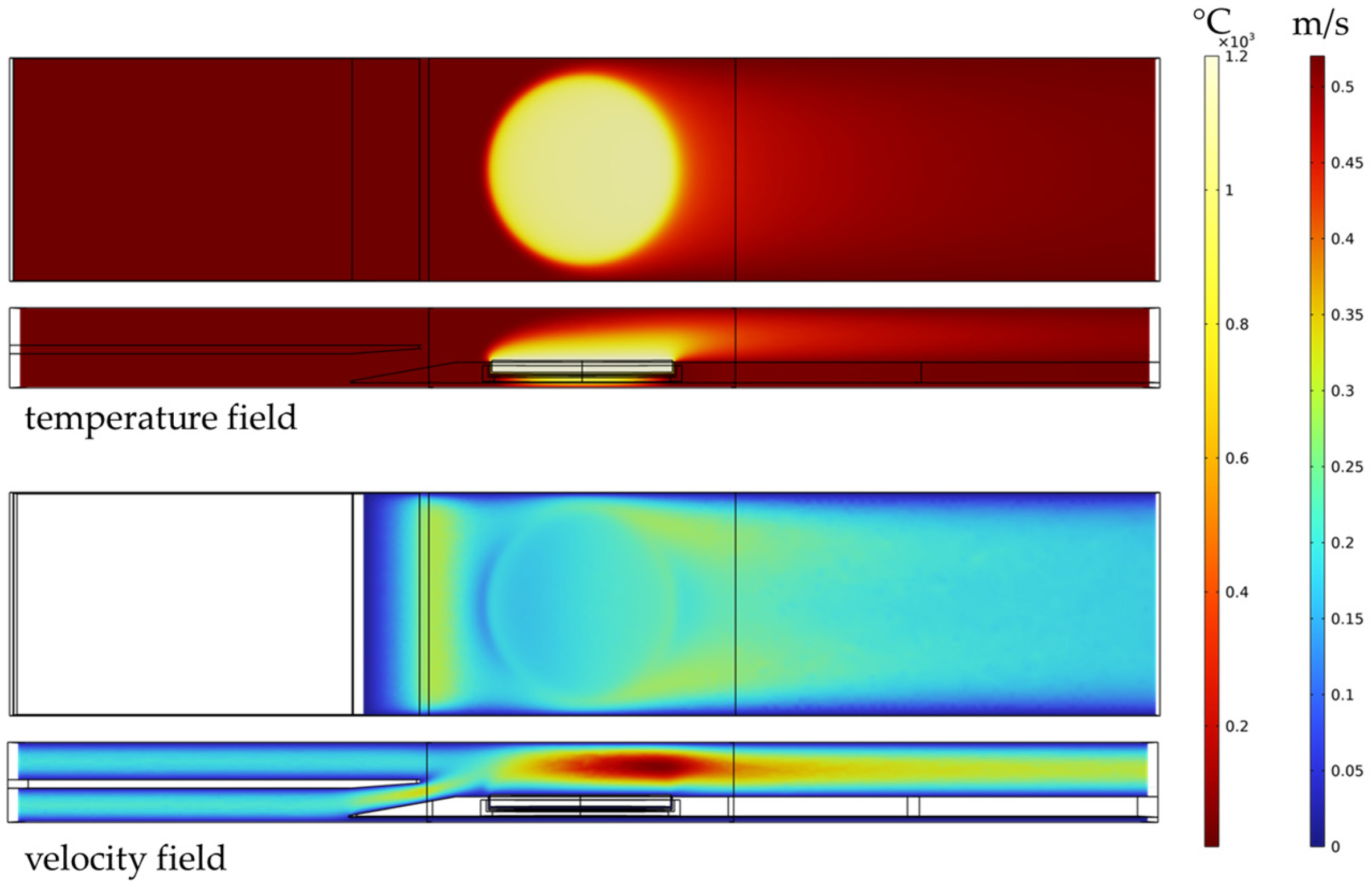
To quantify the difference in the temperature of the carbon-containing gas species, the old quartz and new ceramic susceptor carrier setup was simulated using COMSOL Multiphysics. The model includes the temperature field and laminar flow. The results can be seen in Figure 3 and Figure 4. Figure 3 depicts the calculated temperature field and the velocity of the gas flow in case of the water-cooled quartz susceptor carrier. Furthermore, the difference of temperature between the ceramic and the quartz holder is displayed in Figure 4a. It is obvious that the temperature of the front part of the ceramic carrier is much higher than the one of the quartz carrier. In Figure 4b, the temperature progression of the propane gas flux is depicted. The exact location where the data is taken from is denoted as the grey line in Figure 4a, set to 1 mm above the graphite susceptor plate. The temperature of the epitaxial run using the ceramic susceptor carrier was set slightly lower at 1120 °C instead of 1200 °C to retain CMOS compatibility for the 3C-on-SOI epitaxial runs. In case of the quartz susceptor carrier, the propane gas temperature stays at 20 °C until it reaches the edge of the graphite susceptor plate (x = 82 mm), where the temperature sharply increases to temperatures above 1000 °C. The gas flux flowing over the ceramic susceptor carrier consistently heats up before it reaches the edge of the graphite plate at 82 mm. As a consequence, the propane gas reaches high temperatures faster when the ceramic susceptor carrier is utilized.

3.2. Comparison of Growth Rate

The cross-sections of samples A and B are displayed in Figure 5, respectively. Sample A was grown utilizing the standard quartz susceptor carrier at 1200 °C with a growth rate of 237 nm/h. Sample B is shown in Figure 5b and was grown utilizing the ceramic susceptor carrier at 1120 °C with a growth rate of 492 nm/h. For both samples, the C/Si ratio was set to 6.8 with an effective flow rate of 0.66 sccm SiH4 and 1.49 sccm C3H8. The carrier gas H2 was set to 2154 sccm in total. Despite the lower growth temperature, sample B grew with a significantly higher growth rate, increased by a factor of 2.1. Since SiH4 decomposes easily at elevated temperatures above 300 °C, the main limiting factor for growth rate is the availability of carbon and the rate of adsorption in the boundary layer above the substrate [7,8,9].
We can calculate the total numbers of carbon atoms theoretically available for growth and compare that to the amount of carbon atoms necessary to enable the respective growth rates seen for sample A and B. All samples were grown for 60 min on a square 1-inch substrate. If no adsorption happened on the graphite susceptor itself and only on the substrate with a 1.49 sccm propane flow, only 0.049% of incoming carbon would incorporate into the epitaxial layer, as was the case in sample A, while this number would increase to 0.104% in case of sample B with the ceramic holder. If the heated surface of the graphite susceptor is included and it is assumed that the layer exhibits the same thickness as the substrate itself, the percentages would change to 0.690% and 1.475%, respectively. Since a cold-wall CVD reactor is utilized, the deposition on the reactor’s walls is negligible. It is evident that the low temperatures brought on by the cooling water needed for the system are the primary cause restricting the growth rate, as they lower the amount of carbon accessible due to insufficient fission. Nevertheless, the ceramic non-cooled susceptor carrier increases the amount of carbon cracking compared with the quartz susceptor carrier.

3.3. Characterization of Epitaxial Layers

All five 1-inch samples, A–E shown in Figure 6, were characterized by Raman, EDX and XRD. We investigated the impact of the changed temperature field caused by the different type of susceptor holder on the epitaxial layer by comparing sample A and sample B. Furthermore, samples B, C and D were characterized to examine the influence of the C/Si ratio in combination of the ceramic susceptor holder. Lastly, sample E, grown with the same parameters as sample B, except for the substrate type, was investigated.

3.3.1. Impact of the Susceptor Carrier Type

As shown in the previous chapter, the growth rate more than doubled using the new ceramic susceptor carrier instead of the water-cooled quartz susceptor carrier, despite the lower growth temperature. Figure 7a shows the XRD measurements of sample A and B. Both samples show distinct 3C-SiC peaks in the (200) plane, indicating a single crystalline growth of cubic SiC on Si. Despite a higher film thickness of sample B, the FWHM of the (200) peak is much higher (1.321°) than that of sample A (0.317°), implying a decreased crystalline quality. The additional observation of the (222) peak in sample B indicates that this sample is polycrystalline. Since the process parameters of SiH4 and C3H8 gas flow were kept the same and the growth rate increased nevertheless, we can assume that an increased amount of carbon is being incorporated into the epitaxial layer, shifting the C/Si ratio of the SiC layer above stochiometric parity. To conclude, a decrease of the propane gas flow is needed to improve the crystalline quality if the ceramic susceptor holder is utilized.
Figure 7b and 7c depict cross-sectional EDX measurements of samples A and B. They show that the carbon content of the surface layer is much higher in the case of sample B, reinforcing the assumption that the ceramic holder increases the amount of available carbon in the gas phase. The measured oxygen content is caused by oxidation of the sample after the epitaxial process is concluded. In addition to the increased carbon amount, it is also apparent that the ceramic holder is not incorporating Al atoms into the sample during the growth process since no Al could be detected.

3.3.2. Impact of C/Si Ratio

Sample B, C and D were grown with different C/Si ratios and characterized by Raman spectroscopy to quantify the impact on the crystalline quality. Figure 8a depicts the Raman shift between 700–1100 cm−1 of sample B, C and D, encompassing the TO and LO peak of 3C-SiC at 796 cm−1 and 972 cm−1 [11]. There is a clear trend visible with an increasing C/Si ratio. The LO and the TO peak of 3C-SiC decreases the higher the C/Si ratio is elevated. Sample D with the highest C/Si ratio of 13.2 shows essentially no 3C-SiC TO or LO intensities at all. This is contrary to the observation of Wilhelm et al., who reported an increasing LO/TO ratio in combination with high C/Si ratios. Furthermore, he linked an increasing LO- and decreasing TO peak to higher layer qualities [12].
In Figure 8b, the results of the XRD measurements of samples B, C and D are shown. Sample D with the highest C/Si ratio of 13.2 shows almost no 3C-SiC peaks at all except for the (111) and (222) peak, matching the results of the Raman measurements. Sample B grown with the intermediate C/Si ratio features the (200) and (400) peaks, indicating monocrystalline growth on the (100) substrate. Sample C grown with the lowest C/Si ratio also displays these peaks, however, there is also the (111) peak, the (220) peak and the (222) peak present, indicating polycrystalline growth.

3.3.3. Growth of 3C-SiC-on-SOI

Growth on an SOI substrate was concluded with the same parameters as for sample B on Si substrate. The only difference lies in the extended cool-down period to prevent delamination of the epitaxial layer from the SOI substrate. In Figure 9a, an SEM image of a cross-section of sample E is depicted. The epitaxial layer features a smooth surface and no void structures below the deposited layer could be found. The Raman measurements seen in Figure 9b show a TO peak as well as an LO peak, although the intensity is quite low compared to those of sample B (Figure 8a). On the other hand, the XRD measurements, as shown in Figure 9c, confirm a single crystalline 3C-SiC layer, with an FWHM of 1.066°, slightly better than the one of sample B (1.321°), although still worse than the one of sample A (0.317°). The growth rate was similar to samples B–D.

4. Discussion

The difference in quality between sample A grown with the water-cooled quartz susceptor carrier and sample B grown with the non-cooled ceramic susceptor carrier can be explained by the assumed increased availability of carbon in the boundary layer during the process above the substrate. Kollmuß et al. reported the same tendency while increasing the propane gas flux of 3C-SiC CVD processes [13]. He assumed that a higher propane gas flow leads to an increased number of 2D-SiC nuclei. This was accompanied with an increased growth rate, also seen in this work with all processes utilizing the ceramic susceptor carrier. Furthermore, the growth rate for sample B-E was observed to be similar in all processes, despite the different C3H8 gas flow rates. Chassagne et al. postulates that the growth rate is mainly dependent on the amount of SiH4 flow, which was constant for all processes carried out in the present work [14]. However, his growth temperatures were set to up to 1350 °C instead of the 1120 °C utilized for our samples, so the growth conditions can only be compared with caution.
It was also observed in the Raman measurements of samples B-D that the LO/TO ratio will increase with a decreased C3H8 gas flow rate. This is in direct contrast to the findings of Wilhelm et al., who reported the opposite effect [12]. The EDX measurements of sample A and B indicate that the ceramic susceptor carrier leads to an increased carbon cracking compared to the process with the quartz susceptor carrier. Due to this, the actual C/Si ratio is most likely higher than the intended ratio by the original process parameters. We assume that the C/Si ratio in the boundary layer is much higher for all processes employing the ceramic susceptor carrier. By reducing that imbalance, the quality of the deposited layer was improved.
Utilizing the growth parameters with slight adjustments, we could successfully deposit 3C-SiC on SOI substrates at 1120 °C. The XRD measurements of sample E illustrated in Figure 9b indicate that single crystalline 3C-SiC was grown on top of the SOI layer without delamination. There is still work to do to improve the crystalline quality of the deposited 3C layer, as the Raman measurements as well as the XRD measurements both indicate that the layer is of lower quality than desired. This could be performed by further reducing the C/Si ratio in the process or adjusting the length and the temperature of the carbonization step.

Author Contributions

Conceptualization, J.S. (Johannes Steiner), J.S. (Jana Schultheiß) and P.J.W.; methodology, J.S. (Johannes Steiner), J.S. (Jana Schultheiß) and P.J.W.; software, J.S. (Johannes Steiner) and S.W.; formal analysis, J.S. (Johannes Steiner), J.S. (Jana Schultheiß) and S.W.; investigation, J.S. (Johannes Steiner); writing—original draft preparation, J.S. (Johannes Steiner); writing—review and editing, J.S. (Jana Schultheiß) and P.J.W.; visualization, J.S. (Johannes Steiner); supervision, P.J.W.; project administration, P.J.W.; funding acquisition, P.J.W. All authors have read and agreed to the published version of the manuscript.

Funding

Funding has been provided by the European Union’s Horizon 2020 research and innovation program under grant agreement No. 899679 (SiComb).

Data Availability Statement

Data is contained within the article.

Acknowledgments

Financial support by the European Union’s Horizon 2020 research and innovation program under grant agreement No. 899679 (SiComb).

Conflicts of Interest

The authors declare no conflict of interest.

References

  1. Stern, L.; Stone, J.R.; Kang, S.; Cole, D.C.; Suh, M.G.; Fredrick, C.; Newman, Z.; Vahala, K.; Kitching, J.; Diddams, S.A.; et al. Direct Kerr frequency comb atomic spectroscopy and stabilization. Sci. Adv. 2020, 6, eaax6230. [Google Scholar] [CrossRef]
  2. Fan, T.; Moradinejad, H.; Wu, X.; Eftekhar, A.A.; Adibi, A. High-Q integrated photonic microresonators on 3C-SiC-on-insulator (SiCOI) platform. Opt. Express 2018, 26, 25814–25826. [Google Scholar] [CrossRef] [PubMed]
  3. Levinshtein, M.E.; Rumyantsev, S.L.; Shur, M.S. Properties of Advanced Semiconductor Materials: GaN, AIN, InN, BN, SiC, SiGe; John Wiley & Sons: Hoboken, NJ, USA, 2001. [Google Scholar]
  4. Malitson, I.H. Interspecimen Comparison of the Refractive Index of Fused Silica. J. Opt. Soc. Am. 1965, 55, 1205–1209. [Google Scholar] [CrossRef]
  5. Wischmeyer, F.; Wondrak, W.; Leidich, D.; Niemann, E. CVD growth of 3C-SiC on SOI (100) substrates with optimized interface structure. Mater. Sci. Eng. B 1999, 61–62, 563–566. [Google Scholar] [CrossRef]
  6. Sze, S.M. Semiconductor Devices, Physics and Technology; John Wiley & Sons: Hoboken, NJ, USA, 2001. [Google Scholar]
  7. Hogness, T.R.; Wilson, T.L.; Johnson, W.C. The Thermal Decomposition of Silane. J. Am. Chem. Soc. 2002, 58, 108–112. [Google Scholar] [CrossRef]
  8. Babushok, V.I.; Tsang, W.; Burgess, D.R.; Zachariah, M.R. Numerical study of low- and high-temperature silane combustion. Symp. (Int.) Combust. 1998, 27, 2431–2439. [Google Scholar] [CrossRef]
  9. Pierson, H.O. Handbook of Chemical Vapor Deposition: Principles, Technology and Applications; William Andrew: Norwich, NY, USA, 1999. [Google Scholar]
  10. Iwanowski, R.J.; Fronc, K.; Paszkowicz, W.; Heinonen, M. XPS and XRD study of crystalline 3C-SiC grown by sublimation method. J. Alloys Compd. 1999, 286, 143–147. [Google Scholar] [CrossRef]
  11. Nakashima, S.; Harima, H. Raman investigation of SiC polytypes. Phys. Status Solidi A-Appl. Res. 1997, 162, 39–64. [Google Scholar] [CrossRef]
  12. Wilhelm, M.; Rieth, M.; Brandl, M.; Wibowo, R.A.; Hock, R.; Wellmann, P. Optimization of growth parameters for growth of high quality heteroepitaxial 3C–SiC films at 1200 °C. Thin Solid Film. 2015, 577, 88–93. [Google Scholar] [CrossRef]
  13. Kollmuss, M.; Köhler, J.; Ou, H.Y.; Fan, W.C.; Chaussende, D.; Hock, R.; Wellmann, P.J. Chemical Vapor Deposition of 3C-SiC on [100] Oriented Silicon at Low Temperature < 1200 °C for Photonic Applications. Mater. Sci. Forum 2022, 1062, 119–124. [Google Scholar] [CrossRef]
  14. Chassagne, T.; Ferro, G.; Chaussende, D.; Cauwet, F.; Monteil, Y.; Bouix, J. A comprehensive study of SiC growth processes in a VPE reactor. Thin Solid Film. 2002, 402, 83–89. [Google Scholar] [CrossRef]
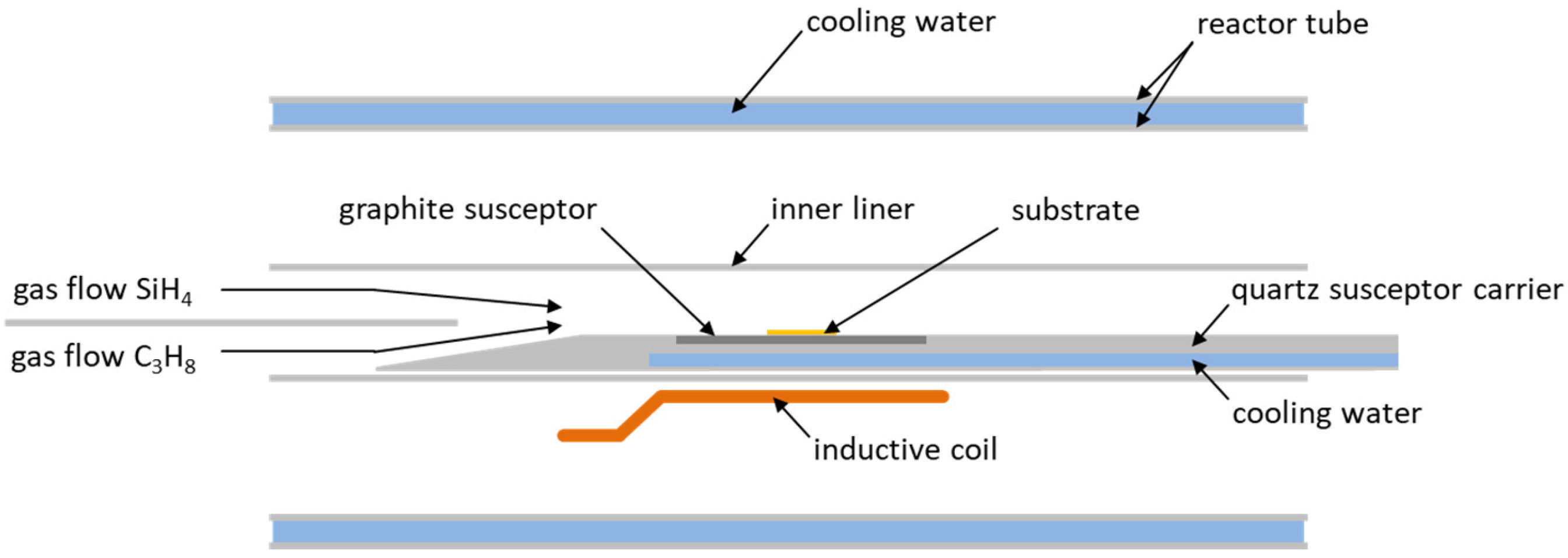
Figure 1. Schematic of the CVD reactor setup with a water-cooled susceptor carrier.
Crystals 13 01590 g001
Figure 2. (a) Al2O3 part including the internal gas line for susceptor rotation; (b) steel part of the redesigned susceptor carrier. In addition to the gas line for susceptor rotation, the steel part exhibits pipes for cooling water.
Crystals 13 01590 g002
Figure 3. Results of the numerical modeling of the water-cooled quartz susceptor carrier and its temperature and velocity field, respectively.
Crystals 13 01590 g003
Figure 4. (a) Calculated temperature fields of the ceramic and quartz holder, respectively. The black arrows denote the gas flow. The grey line marks the position of the temperature data, which is illustrated in (b).
Crystals 13 01590 g004
Figure 5. (a) Cross-section of sample A grown with the quartz susceptor carrier at 1200 °C. The thickness is measured to be 237 nm; (b) Cross-section of sample B grown with the ceramic susceptor carrier at 1120 °C. The thickness was measured to be 492 nm.
Crystals 13 01590 g005
Figure 6. Images of the grown epitaxial layers. (ad) Samples A–D grown on a Si substrate; (e) Sample E grown on a SOI substrate. The black shadows on (b,d,e) are reflections and not part of the surface morphology.
Crystals 13 01590 g006
Figure 7. (a) XRD measurements of the grown epitaxial layers A and B. The yellow dashed lines indicate specific peaks typical for 3C-SiC [10]. The sharp peaks at 33° and 62° and the distinctive peak at 70° belong to the Si substrate; (b) EDX measurements of a cross-section of sample A; (c) EDX measurements of a cross-section of sample B.
Crystals 13 01590 g007
Figure 8. (a) Raman measurements of the Si substrate and sample B, C and D grown with a C/Si ratio of 6.8, 3.4 and 13.2, respectively; (b) XRD measurements of samples B, C and D. The yellow dashed lines indicate specific peaks typical for 3C-SiC [10]. The sharp peaks at 33° and 62° and the distinctive peak at 70° belong to the Si substrate.
Crystals 13 01590 g008
Figure 9. (a) SEM image of cross-section of sample E; (b) Raman measurement of sample E; (c) XRD measurements of sample E. The yellow dashed lines indicate specific peaks typical for 3C-SiC [10]. The sharp peaks at 33° and 62° and the distinctive peak at 70° belong to the SOI substrate.
Crystals 13 01590 g009
Table 1. Overview of all grown samples with varied key parameters.
Sample NameSubstrate TypeSusceptor Carrier TypeProcess Temperature [°C]C/Si RatioGrowth Rate [nm/h]
sample ASiquartz12006.8237
sample BSiceramic11206.8492
sample CSiceramic11203.4650
sample DSiceramic112013.2615
sample ESOIceramic11206.8533
Disclaimer/Publisher’s Note: The statements, opinions and data contained in all publications are solely those of the individual author(s) and contributor(s) and not of MDPI and/or the editor(s). MDPI and/or the editor(s) disclaim responsibility for any injury to people or property resulting from any ideas, methods, instructions or products referred to in the content.