
Wafer-Scale Emission Energy Modulation of Indium Flushed Quantum Dots
by

Nikolai Spitzer
*,
Nikolai Bart
,
Hans-Georg Babin
,
Marcel Schmidt
,
Andreas D. Wieck
and
Arne Ludwig
Lehrstuhl für Angewandte Festkörperphysik, Ruhr-Universität Bochum, Universitätsstraße 150, 44801 Bochum, Germany
*
Author to whom correspondence should be addressed.
Crystals 2023, 13(12), 1657; https://doi.org/10.3390/cryst13121657
Submission received: 31 October 2023
/
Revised: 14 November 2023
/
Accepted: 25 November 2023
/
Published: 30 November 2023
(This article belongs to the Special Issue Modelling of Crystal Growth Processes)
Abstract
:Semiconductor self-assembled quantum dots (QDs) have garnered immense attention for their potential in various quantum technologies and photonics applications. Here, we explore a novel approach for fine-tuning the emission wavelength of QDs by building upon the indium flush growth method: Submonolayer variations in the capping thickness reveal a non-monotonic progression, where the emission energy can decrease even though the capping thickness decreases. indium flush, a well-known technique for inducing blue shifts in quantum dot emissions, involves the partial capping of QDs with GaAs followed by a temperature ramp-up. However, our findings reveal that the capping layer roughness, stemming from fractional monolayers during overgrowth, plays a pivotal role in modulating the emission energy of these QDs. We propose increased indium interdiffusion between the QDs and the surrounding GaAs capping layer for a rough surface surrounding the QD as the driving mechanism. This interdiffusion alters the indium content within the QDs, resulting in an additional emission energy shift, counterintuitive to the capping layer’s thickness increase. We utilize photoluminescence spectroscopy to generate wafer maps depicting the emission spectrum of the QDs. Using thickness gradients, we produce systematic variations in the capping layer thickness on 3″ wafers, resulting in modulations of the emission energy of up to 26 meV.
1. Introduction
Semiconductor self-assembled quantum dots (QDs) obtained by epitaxial growth are excellent single photon sources [1] and promising material systems for applications in quantum communication networks [2], quantum computation, quantum cryptography [3] and photonics [4,5]. QDs and similar low-dimensional electron systems, including nanotubes and 2D materials, play a crucial role in theoretical modulation and simulation. As a result, the growth process of In-based nanostructures and associated structural considerations have been accurately predicted [6,7]. This not only guides experimental work but also lays the foundation for future advancements. Different growth techniques are employed to achieve specific wavelength ranges suitable for applications and characterisation purposes. GaAs/AlGaAs QDs [8,9,10] created by local droplet etching and InAs/GaAs QDs formed via the Stranski–Krastanov growth mode [11] serve as notable examples. Stranski–Krastanov QDs have been extensively studied [12,13] and are well-established as high-quality single photon sources [1]. However, these QDs exhibit a limited emission wavelength range, typically spanning from 1100 nm to 1300 nm. Shifting this wavelength to short values is crucial in order to take advantage of widely used Si-based detectors and make it applicable to devices requiring precise specifications [14,15]. Methods include rapid thermal annealing [16,17], strain-induced material intermixing [18] and indium flushing [19]. Developed by Wasilewski et al. [19], this procedure blue-shifts the emission wavelength by reducing the QD height [20,21]. This involves partially covering of the QDs with GaAs and a subsequent temperature ramp-up, reducing the height of the QDs and thus shifting the wavelength towards the band gap energy of GaAs.
The indium flush technique has undergone extensive research [22], with numerous studies investigating capping layer height [21,23], annealing time [24], substrate temperature [25] and growth rates [26]. Here, we present findings on the influence of partial monolayer surface roughness during the capping layer’s growth phase in the indium flush process. During layer-by-layer growth, the surface state undergoes transitions between complete and fractional monolayer coverage, corresponding to an alternating evolution of smooth and rough surfaces, which is well known from observations during RHEED measurements [27,28]. Our recent findings have shed light on the significance of this surface roughness prior QD growth, showing a strong influence on the QD nucleation [29]. Similarly, during the indium flush process, the capping layer on top of the QDs undergoes the same transitions. Growing the capping layer with a deliberate thickness gradient provides QD capping with complete and incomplete monolayers, resulting in a modulation of the roughness across the wafer. We analyse the ground state emission energy peak of the QD ensemble performing photoluminescence spectroscopy. Across the wafer, we find a deviation from the expected monotonous progression of the emission energy as a function of the capping thickness. Instead, we observe an additional modulation along the gradient. Depending on the surface state of the capping layer, the emission energy can increase, even though the capping thickness increases. This allows us to find multiple capping thicknesses that correspond to the same emission energies.
2. Methods
The growth of self-assembled QDs was carried out using molecular beam epitaxy (MBE) on undoped (100)-oriented 3″ GaAs wafers with a miscut of less than 0.1°. The growth was performed in a modified Riber Epineat III/V S solid-source MBE system. The effusion cells have an inclination angle of 49° between the substrate plane and the cells, as illustrated in Figure 1c. This angle leads to a material gradient across the wafer, with higher deposition rates at the wafer side close to the cells. For layers without intentional gradients, the wafers were rotated during the deposition process. Prior to the growth process, the wafers were deoxidized at 640 °C (measured with a pyrometer) under an arsenic beam equivalent pressure (BEP) of 9.6 × 10⁻⁶ Torr. The standard growth rates were set at 0.2 nm/s for GaAs, 0.1 nm/s for AlAs and 0.3 nm/s for Al0.33Ga0.67As. The temperatures were calibrated using a pyrometer before growth. All GaAs, AlGaAs and AlAs layers were grown at 600 °C under an As BEP of 9.6 × 10⁻⁶ Torr.
The growth of all samples followed the same protocol: A 50 nm GaAs buffer layer was grown first to achieve a smooth surface, followed by a short period superlattice consisting of 30 pairs of 2 nm AlAs and 2 nm GaAs, and another 50 nm GaAs buffer layer. On the one hand, the superlattice stops the segregation of impurities; on the other hand, it smooths the surface and thus reduces the roughness. This was followed by an additional 30 nm of GaAs growth at 600 °C, with a 7-min annealing step for surface smoothing. The substrate temperature was then reduced in two steps: first, to 530 °C in 30 s, with a simultaneous decrease in arsenic BEP to 6.8 × 10⁻⁶ Torr; second, to the QD growth temperature at 515 °C in 1 min. A 1 minute break allowed the temperature to stabilize and the wafer rotation to stop. The indium was deposited in cycles by opening and closing the shutter at 4-s intervals. Typically, 12–13 cycles of indium were deposited, with a growth rate of approximately 0.012 nm/s. The initial four cycles were grown without rotation, increasing the indium flux at the big flat, while the remaining cycles were grown with rotation, achieving coverages ranging from 1.4 to 1.8 monolayers (ML) across the wafer. A 20 s break after indium deposition allows for additional QD formation. As a result, this deposition process typically yielded wafers with QDs covering more than half of the surface area, as illustrated in Figure 1a, where the border between areas with QDs and those without is referred to as the ‘transition’. The substrate temperature was decreased by 50 °C before partially capping the QDs with GaAs. During this process, the GaAs cap was grown without rotation, resulting in a thickness gradient parallel to the big flat, with the highest material concentration observed at the small flat, as depicted in Figure 1b. To cover a broad QD emission wavelength range from 920 nm to 1150 nm, we grew three samples with different GaAs capping gradients, yielding capping thicknesses from 2 nm to 6 nm. Excess InAs was removed by ramping up the temperature to 600 °C in 60 s while simultaneously increasing the As BEP to 9.6 × 10⁻⁶ Torr. The indium flushed QDs were then capped with 6 to 8.5 nm of GaAs, resulting in a total GaAs coverage of 11 nm for all samples. This is followed by 135 nm of Al0.33Ga0.67As. Finally, a 5 nm GaAs cap was grown to minimize oxidation.
The characterization of the QDs was performed using photoluminescence (PL) spectroscopy. For this purpose, a homebuilt setup was employed, consisting of a 3″ copper cold finger within a cryostat. The cryostat is cooled by liquid nitrogen, enabling the temperature to be maintained at approximately 85 K during measurements. For wafer mapping, the entire cryostat was subsequently moved with two step motors. To excite the QDs, a 518 nm laser with a spot size of 100 µm diameter was used, enabling the probing of the collective emission of a QD ensemble. Laser excitation powers between 1 and 5 mW were employed. Using a spectrometer equipped with a Si-CCD detector, the QD emission was measured at wavelengths ranging from 340 nm to 900 nm. Additionally, an InGaAs line array detector was used for wavelengths between 900 nm and 1715 nm.
3. Results
Figure 2a shows the integrated PL intensity counts within the wavelength range of 900–1050 nm, where the QD emission is expected for this sample. Notably, the PL intensity exhibits a distinct cut-off, attributed to the deposition of indium in a gradient fashion, leading to the formation of a transition region separating regions with QDs and those without. The geometry of this transition region mirrors the effusion profile of the indium cell. Above this transition region, the critical InAs layer thickness of 1.5 ML is not attained, preventing the nucleation of QDs [30].
In Figure 2b, spectra along the GaAs coverage gradient extracted from the PL map depicted in Figure 2a are presented. The red dashed line in Figure 2c designates the region from which the spectra were obtained. These spectra show the QD ground state emission at 950–1010 nm and the first excited state at 925–970 nm. The ground state level and the first excited state of the QDs exhibit a high degree of homogeneity within the displayed range. To gain deeper insights into the observed wavelength trends, Gaussian peak fits were applied to the ground state emission from the PL map in Figure 2a. The results of this analysis are illustrated in Figure 2c, revealing a stripe-like pattern that corresponds to non-monotonic behavior of the wavelength. The inset in Figure 2c shows the wavelengths along the red dashed line. Despite the steady increase in QD height—a key factor influencing emission wavelength—the gradient along the x-direction exhibits a distinctive pattern characterized by a slope superimposed with a sinusoidal-like function.
We propose that the wavelength modulation arises as a consequence of the surface roughness modulation induced by submonolayers, which naturally occurs during the growth process when rotation is halted. The process is schematically illustrated in Figure 3. A rough surface has the capacity to facilitate the incorporation of segregating indium into an InGaAs alloy situated at the surface. Figure 3c demonstrates the migration of indium from the tops of the QDs during the initial reduction in height within the first capping regime [26,31]. The migrating indium forms an InGaAs wall around the QDs as depicted in Figure 3b. During heating, the InGaAs ring diffuses and spreads over the surface, with the rough surface around the QD incorporating more of the indium-rich material in its vicinity as illustrated in Figure 3d. The surface’s inherent roughness provides statistically more monolayer steps [29], thus offering an increased number of binding sites for InAs to integrate into the surface. Consequently, this phenomenon makes sublimation less probable. The higher indium content resulting from this process serves to decrease InGa interdiffusion in the QD. Another effect that takes place is the reduction of strain in the QD due to the higher indium content in the surrounding InGaAs layer. The reduction in strain effectively accelerates the onset of the second capping phase, during which the QDs are capped by GaAs, resulting in higher InGa interdiffusion [31]. Which of the two mechanisms is dominant cannot be clarified with the present measured data. Nevertheless, the modulation periods should correspond to the count of integer GaAs capping thickness, measured in monolayers across the entire wafer.
To determine the capping thickness as a function of the location on the wafer, we utilized a position-dependent growth rate simulation of the gallium effusion cell profile based on optical measurements of AlAs/GaAs quantum well samples. Thickness distributions of the GaAs coverage on QDs prior to the flushing step are shown for three samples in Figure 2d, Figure 4d and Figure A1d, respectively. The shape and the modulation period match the observed modulation in Figure 2c, Figure 4a and Figure A1a. Sample #15633’s results further affirm the agreement between simulation and measured data, as shown in the Figure 4d. Across the wafer, the thickness of the capping layer varies between 6 and 10 ML of GaAs. The QDs emit between 900 and 980 nm, as evident in the waterfall plot in Figure 4b. The observed wavelength modulation periods appear to match with the number of different integer monolayers. With a capping difference of four monolayers of GaAs on the wafer, the gradient plot displays four local maxima.
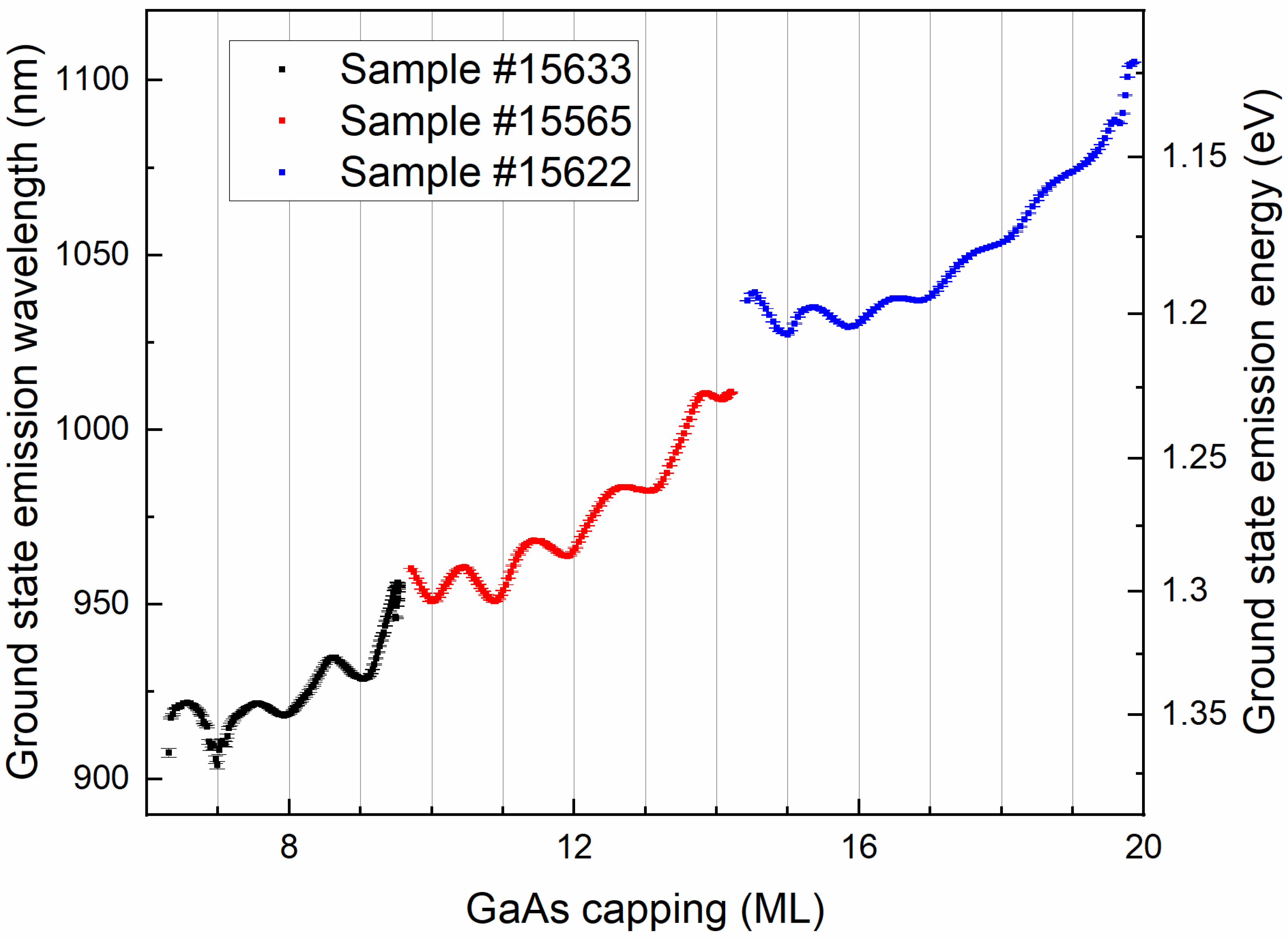
Figure 5 shows the ground state energies of QD emissions plotted against the GaAs coverage of the QDs for all three samples. The measured data correspond to the red dashed lines in Figure 2c, as well Figure 4a and Figure A1a. The modulation of the peak emission energies covers the entire wavelength range, extending from 900 nm to 1100 nm. Notably, the amplitude of this modulation diminishes as the GaAs coverage layers increase in size. This phenomenon aligns with expectations because a larger coverage layer results in a smaller interaction area of a QD with the GaAs surface. Furthermore, the influence of indium segregation diminishes as capping layers become thicker. The gradient of all three wafers shows a red shift at the edge, which corresponds to the largest and smallest GaAs capping, respectively, that deviates from the overall trend. This behavior can be explained by the inhomogeneous heat distribution on the wafer. At the edge of the wafer, the temperature is lower so that less indium diffuses from the QD during the flush process. The gridlines on the graph indicate a strong correspondence between the simulation and experimental data across the entire investigated emission spectrum.
4. Conclusions
In conclusion, this study underscores the significance of the growth phase in the indium flush method, a pivotal technique for in-situ QD treatment. A key discovery in this research is the occurrence of a roughness modulation, primarily induced by fractional monolayers during the gradient overgrowth of QDs, which results in a modulation of the ground state energy, with fluctuations of up to 26 meV. We observe the effect consistently across the entire wavelength range, spanning from 900 nm to 1100 nm. This corresponds to flushed QDs with heights ranging from 2 nm to 6 nm. Notably, the effect diminishes for longer wavelengths.
This phenomenon can be tentatively explained by the heightened interdiffusion between the QDs and the surface in the presence of a rough surface. The roughness, by providing additional binding sites, seemingly facilitates the diffusion of indium from the QD.
The observed effect demonstrates the importance of the growth phase not only for the subsequent grown structures [9,29], but also for the material transport and arrangement of atomic steps during annealing breaks. The seemingly subtle effect of the periodically evolving growth phase thus becomes not only strongly evident in the nucleation of QDs [9,30], but also in the emission properties of flushed QDs. The observed effect is expected to extend its influence to the indium flush process and, more broadly, to double capping techniques involving other material systems, such as InAs/InP [32].
However, it is important to note that for a precise and comprehensive understanding of this effect, further investigations are needed. Utilizing imaging techniques, particularly transmission electron microscopy, will be instrumental in deciphering both the size and composition of the QDs, enabling a more detailed and accurate explanation.
Furthermore, future research should delve into the prospect of contrasting the optical characteristics of QDs featuring different GaAs coverages while maintaining similar emission energies. Employing techniques such as micro-PL not only promises to yield valuable insights into the optical behaviors of these QDs, such as transition and level energies, optical recombination rate and Auger rate [33], but may also unlock novel methods for enhancing QD applications in terms of quantum and spin coherence or susceptibility to charge noise.
Author Contributions
Conceptualization, N.S., N.B. and A.L.; methodology, N.S. and N.B.; software, M.S.; validation, N.S., N.B. and A.L.; formal analysis, N.S., N.B., H.-G.B. and A.L.; investigation, N.S. and N.B.; resources, A.D.W. and A.L.; data curation, N.S.; writing—original draft preparation, N.S. and N.B.; writing—review and editing, N.S., N.B., H.-G.B., A.D.W. and A.L.; visualization, N.S.; supervision, N.S., A.D.W. and A.L.; project administration, A.D.W. and A.L.; funding acquisition, A.D.W. and A.L. All authors have read and agreed to the published version of the manuscript.
Funding
We gratefully acknowledge financial support from the grants DFH/UFA CDFA05-06, DFG TRR160, DFG project 383065199, EU Horizon 2020 Grant No. 861097, Federal Ministry of Education and Research (BMBF) QR.X Project 16KISQ009, 16KISQ027BMBF and Q.Link.X 16KIS0867.
Data Availability Statement
The data presented in this study are openly available in FigShare at 10.6084/m9.figshare.24665622.
Conflicts of Interest
The authors declare no conflict of interest.
Appendix A
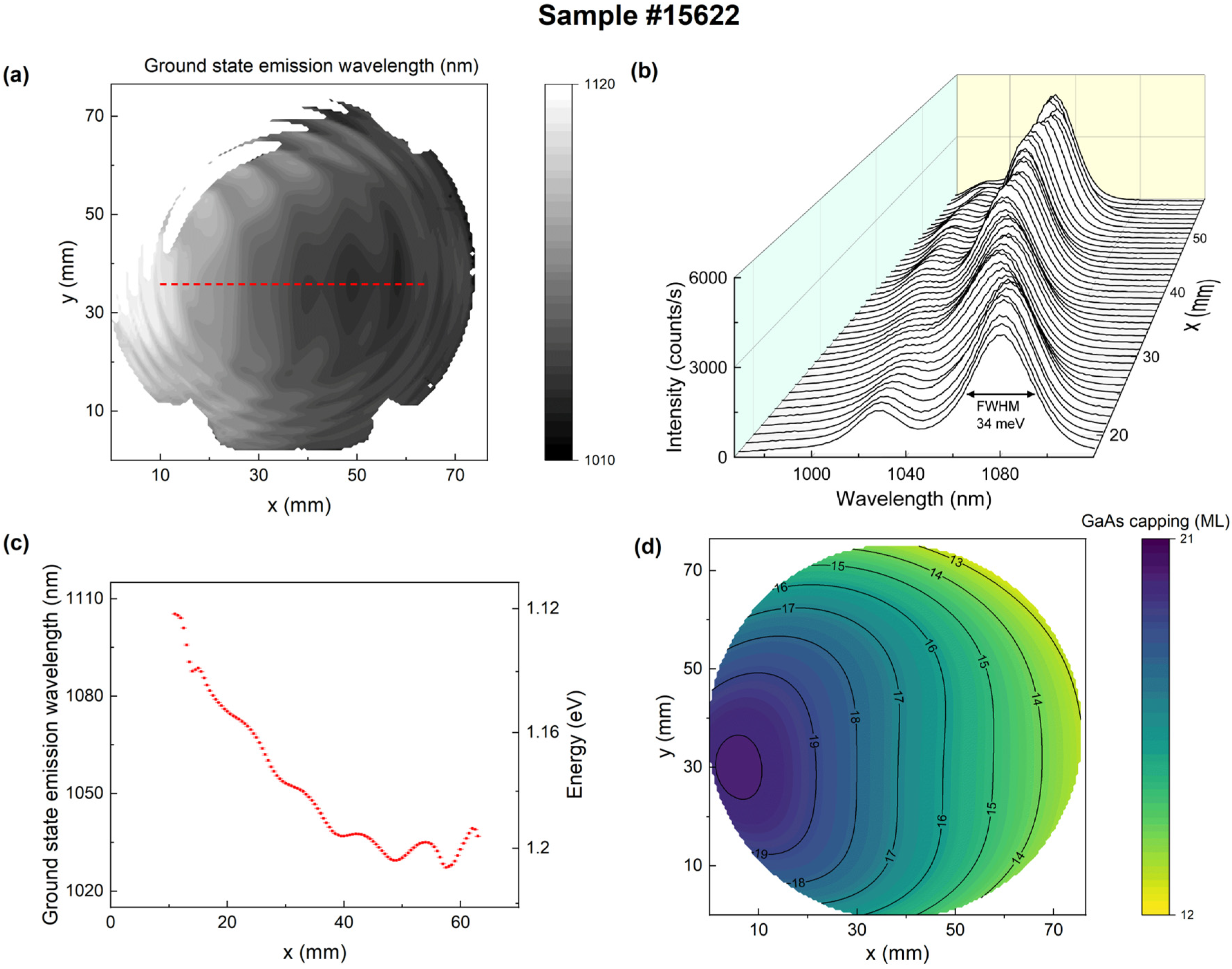
Figure A1.
PL measurements of sample #15622 with a flushing gradient from 21 to 12 ML. (a) The wafer map displays the ground state QD emission wavelength, which was extracted through Gaussian fitting of the PL data. The modulation at the edge of the wafer is another effect described by us in an earlier publication. The growth phase of the substrate on which the QDs are grown has an influence on density and emission energy [29]. (b) A waterfall plot illustrating the PL spectra taken at the gradient along y = 36 mm marked with a dashed line in (a). (c) The ground state emission wavelength and energy along the dashed line in (a). (d) Simulation of the GaAs capping thickness on the wafer.
References
- Tomm, N.; Javadi, A.; Antoniadis, N.O.; Najer, D.; Löbl, M.C.; Korsch, A.R.; Schott, R.; Valentin, S.R.; Wieck, A.D.; Ludwig, A.; et al. A bright and fast source of coherent single photons. Nat. Nanotechnol. 2021, 16, 399–403. [Google Scholar] [CrossRef] [PubMed]
- The Nobel Prize in Chemistry 2023. NobelPrize.org. Nobel Prize Outreach AB 2023. Mon. 16 October 2023. Available online: https://www.nobelprize.org/prizes/chemistry/2023/summary/ (accessed on 13th October 2023).
- Kuhlmann, A.V.; Houel, J.; Ludwig, A.; Greuter, L.; Reuter, D.; Wieck, A.D.; Poggio, M.; Warburton, R.J. Charge noise and spin noise in a semiconductor quantum device. Nat. Phys. 2013, 9, 570–575. [Google Scholar] [CrossRef]
- Shchekin, O.B.; Deppe, D.G. 1.3 μm InAs quantum dot laser with To=161 K from 0 to 80 °C. Appl. Phys. Lett. 2002, 80, 3277–3279. [Google Scholar] [CrossRef]
- Newell, T.C.; Bossert, D.J.; Stintz, A.; Fuchs, B.; Malloy, K.J.; Lester, L.F. Gain and linewidth enhancement factor in InAs quantum-dot laser diodes. IEEE Photonics Technol. Lett. 1999, 11, 1527–1529. [Google Scholar] [CrossRef]
- Alves Machado Filho, M.; Hsiao, C.-L.; Dos Santos, R.B.; Hultman, L.; Birch, J.; Gueorguiev, G.K. Self-Induced Core-Shell InAlN Nanorods: Formation and Stability Unraveled by Ab Initio Simulations. ACS Nanosci. Au 2023, 3, 84–93. [Google Scholar] [CrossRef] [PubMed]
- Lundgren, C.; Kakanakova-Georgieva, A.; Gueorguiev, G.K. A perspective on thermal stability and mechanical properties of 2D Indium Bismide from ab initio molecular dynamics. Nanotechnology 2022, 33, 335706. [Google Scholar] [CrossRef]
- Babin, H.G.; Ritzmann, J.; Bart, N.; Schmidt, M.; Kruck, T.; Zhai, L.; Löbl, M.C.; Nguyen, G.N.; Spinnler, C.; Ranasinghe, L.; et al. Charge Tunable GaAs Quantum Dots in a Photonic n-i-p Diode. Nanomaterials 2021, 11, 2703. [Google Scholar] [CrossRef] [PubMed]
- Babin, H.-G.; Bart, N.; Schmidt, M.; Spitzer, N.; Wieck, A.D.; Ludwig, A. Full wafer property control of local droplet etched GaAs quantum dots. J. Cryst. Growth 2022, 591, 126713. [Google Scholar] [CrossRef]
- Heyn, C.; Stemmann, A.; Hansen, W. Dynamics of self-assembled droplet etching. Appl. Phys. Lett. 2009, 95, 173110. [Google Scholar] [CrossRef]
- Leonard, D.; Krishnamurthy, M.; Reaves, C.M.; Denbaars, S.P.; Petroff, P.M. Direct formation of quantum-sized dots from uniform coherent islands of InGaAs on GaAs surfaces. Appl. Phys. Lett. 1993, 63, 3203–3205. [Google Scholar] [CrossRef]
- Passow, T.; Li, S.; Feinäugle, P.; Vallaitis, T.; Leuthold, J.; Litvinov, D.; Gerthsen, D.; Hetterich, M. Systematic investigation into the influence of growth conditions on InAs/GaAs quantum dot properties. J. Appl. Phys. 2007, 102, 073511. [Google Scholar] [CrossRef]
- Rosenauer, A.; Gerthsen, D.; van Dyck, D.; Arzberger, M.; Böhm, G.; Abstreiter, G. Quantification of segregation and mass transport in InxGa1−xAs/GaAs Stranski-Krastanow layers. Phys. Rev. B 2001, 64, 245334. [Google Scholar] [CrossRef]
- Haffouz, S.; Raymond, S.; Lu, Z.G.; Barrios, P.J.; Roy-Guay, D.; Wu, X.; Liu, J.R.; Poitras, D.; Wasilewski, Z.R. Growth and fabrication of quantum dots superluminescent diodes using the indium-flush technique: A new approach in controlling the bandwidth. J. Cryst. Growth 2009, 311, 1803–1806. [Google Scholar] [CrossRef]
- Hino, Y.; Ozaki, N.; Ohkouchi, S.; Ikeda, N.; Sugimoto, Y. Growth of InAs/GaAs quantum dots with central emission wavelength of 1.05 μm using In-flush technique for broadband near-infrared light source. J. Cryst. Growth 2013, 378, 501–505. [Google Scholar] [CrossRef]
- Fafard, S.; Allen, C.N. Intermixing in quantum-dot ensembles with sharp adjustable shells. Appl. Phys. Lett. 1999, 75, 2374–2376. [Google Scholar] [CrossRef]
- Perret, N.; Morris, D.; Franchomme-Fossé, L.; Côté, R.; Fafard, S.; Aimez, V.; Beauvais, J. Origin of the inhomogenous broadening and alloy intermixing in InAs/GaAs self-assembled quantum dots. Phys. Rev. B 2000, 62, 5092–5099. [Google Scholar] [CrossRef]
- Lipinski, M.O.; Schuler, H.; Schmidt, O.G.; Eberl, K.; Jin-Phillipp, N.Y. Strain-induced material intermixing of InAs quantum dots in GaAs. Appl. Phys. Lett. 2000, 77, 1789–1791. [Google Scholar] [CrossRef]
- Wasilewski, Z.R.; Fafard, S.; McCaffrey, J.P. Size and shape engineering of vertically stacked self-assembled quantum dots. J. Cryst. Growth 1999, 201–202, 1131–1135. [Google Scholar] [CrossRef]
- Fafard, S.; Wasilewski, Z.R.; Allen, C.N.; Picard, D.; Spanner, M.; McCaffrey, J.P.; Piva, P.G. Manipulating the energy levels of semiconductor quantum dots. Phys. Rev. B 1999, 59, 15368–15373. [Google Scholar] [CrossRef]
- Fafard, S.; Wasilewski, Z.R.; Allen, C.N.; Hinzer, K.; McCaffrey, J.P.; Feng, Y. Lasing in quantum-dot ensembles with sharp adjustable electronic shells. Appl. Phys. Lett. 1999, 75, 986–988. [Google Scholar] [CrossRef]
- Molas, M.; Gołasa, K.; Kuldová, K.; Borysiuk, J.; Babiński, A.; Lapointe, J.; Wasilewski, Z.R. The effect of In-flush on the optical anisotropy of InAs/GaAs quantum dots. J. Appl. Phys. 2012, 111, 33510. [Google Scholar] [CrossRef]
- Keizer, J.G.; Clark, E.C.; Bichler, M.; Abstreiter, G.; Finley, J.J.; Koenraad, P.M. An atomically resolved study of InGaAs quantum dot layers grown with an indium flush step. Nanotechnology 2010, 21, 215705. [Google Scholar] [CrossRef]
- Wang, L.; Rastelli, A.; Schmidt, O.G. Structural and optical properties of In(Ga)As/GaAs quantum dots treated by partial capping and annealing. J. Appl. Phys. 2006, 100, 064313. [Google Scholar] [CrossRef]
- Kumagai, N.; Ohkouchi, S.; Nakagawa, S.; Nomura, M.; Ota, Y.; Shirane, M.; Igarashi, Y.; Yorozu, S.; Iwamoto, S.; Arakawa, Y. Suppression of indefinite peaks in InAs/GaAs quantum dot spectrum by low temperature capping in the indium-flush method. Phys. E Low-Dimens. Syst. Nanostructures 2010, 42, 2753–2756. [Google Scholar] [CrossRef]
- Costantini, G.; Rastelli, A.; Manzano, C.; Acosta-Diaz, P.; Songmuang, R.; Katsaros, G.; Schmidt, O.G.; Kern, K. Interplay between thermodynamics and kinetics in the capping of InAs/GaAs(001) quantum dots. Phys. Rev. Lett. 2006, 96, 226106. [Google Scholar] [CrossRef]
- Harris, J.J.; Joyce, B.A.; Dobson, P.J. Oscillations in the surface structure of Sn-doped GaAs during growth by MBE. Surf. Sci. Lett. 1981, 103, L90–L96. [Google Scholar] [CrossRef]
- Neave, J.H.; Joyce, B.A.; Dobson, P.J.; Norton, N. Dynamics of film growth of GaAs by MBE from Rheed observations. Appl. Phys. A 1983, 31, 1–8. [Google Scholar] [CrossRef]
- Bart, N.; Dangel, C.; Zajac, P.; Spitzer, N.; Ritzmann, J.; Schmidt, M.; Babin, H.G.; Schott, R.; Valentin, S.R.; Scholz, S.; et al. Wafer-scale epitaxial modulation of quantum dot density. Nat. Commun. 2022, 13, 1633. [Google Scholar] [CrossRef]
- Leonard, D.; Pond, K.; Petroff, P.M. Critical layer thickness for self-assembled InAs islands on GaAs. Phys. Rev. B 1994, 50, 11687–11692. [Google Scholar] [CrossRef]
- Joyce, P.B.; Krzyzewski, T.J.; Bell, G.R.; Jones, T.S. Surface morphology evolution during the overgrowth of large InAs–GaAs quantum dots. Appl. Phys. Lett. 2001, 79, 3615–3617. [Google Scholar] [CrossRef]
- Ulloa, J.M.; Koenraad, P.M.; Gapihan, E.; Létoublon, A.; Bertru, N. Double capping of molecular beam epitaxy grown InAs/InP quantum dots studied by cross-sectional scanning tunneling microscopy. Appl. Phys. Lett. 2007, 91, 073106. [Google Scholar] [CrossRef]
- Kurzmann, A.; Ludwig, A.; Wieck, A.D.; Lorke, A.; Geller, M. Auger Recombination in Self-Assembled Quantum Dots: Quenching and Broadening of the Charged Exciton Transition. Nano Lett. 2016, 16, 3367–3372. [Google Scholar] [CrossRef]
Figure 1.
(a) Sketch of the indium cell emission profile and the resulting QD density. (b) The direction of the gallium effusion cell during the capping process of the QDs is shown. (c) Drawing of the pseudo cross section through the wafer. The flushed QDs become smaller in the gradient growth method the farther they are from the effusion cell, i.e., the thinner the GaAs capping layer is.
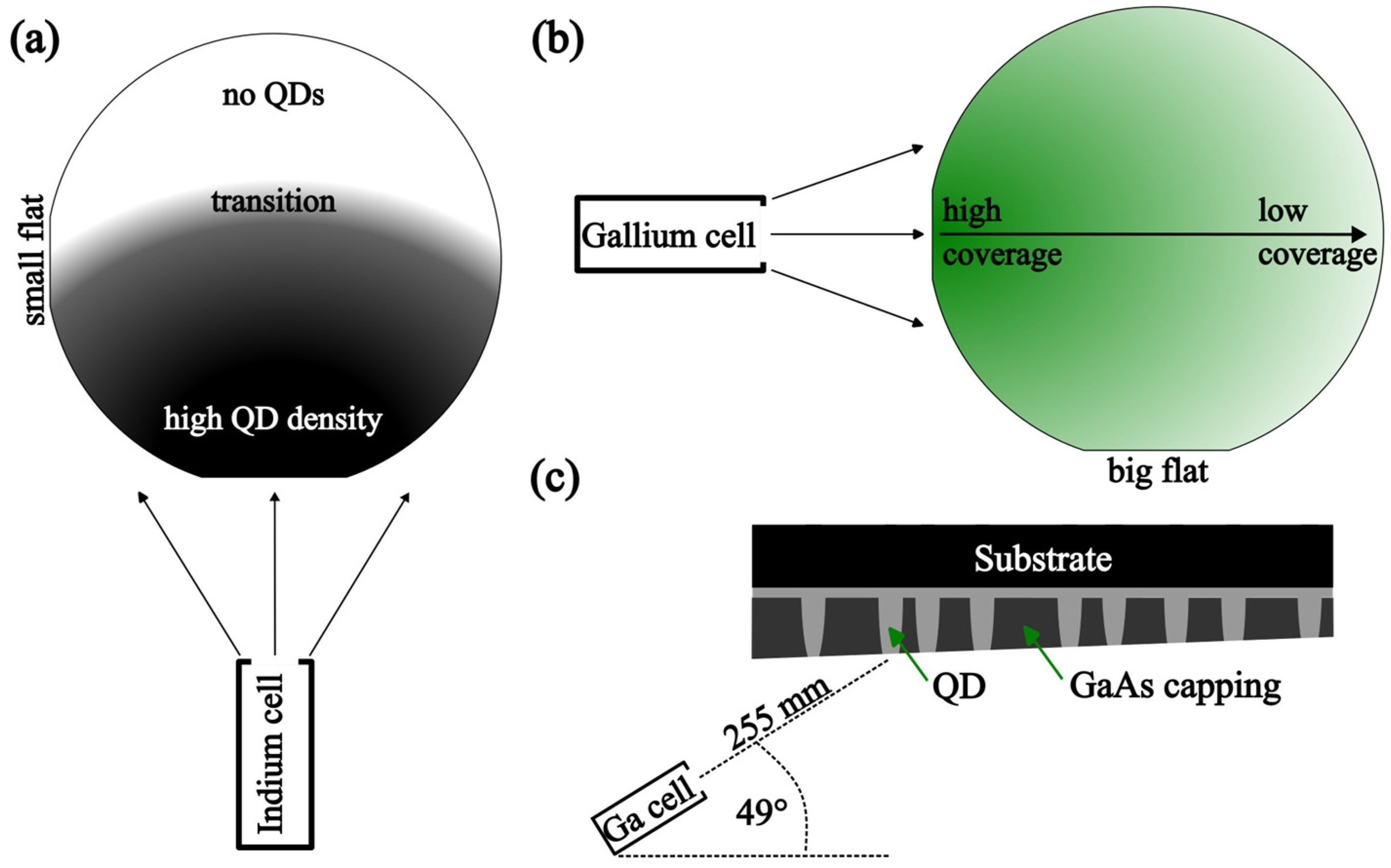
Figure 2.
PL measurements, analysis and growth rate simulation of sample #15565. (a) Wafer map depicting the integrated PL intensity between 900 nm and 1050 nm. (b) PL spectra along the gradient, corresponding to red dashed line in (c). (c) Wafer map of the wavelength of the ground state emission, determined with Gaussian fits. The inset plot shows the wavelengths along the gradient and is marked with the red dotted line at y = 32 mm. (d) Calculated layer thickness for the flush capping layer showing the cell beam profile of the gallium cell with the growth parameters used for the sample.
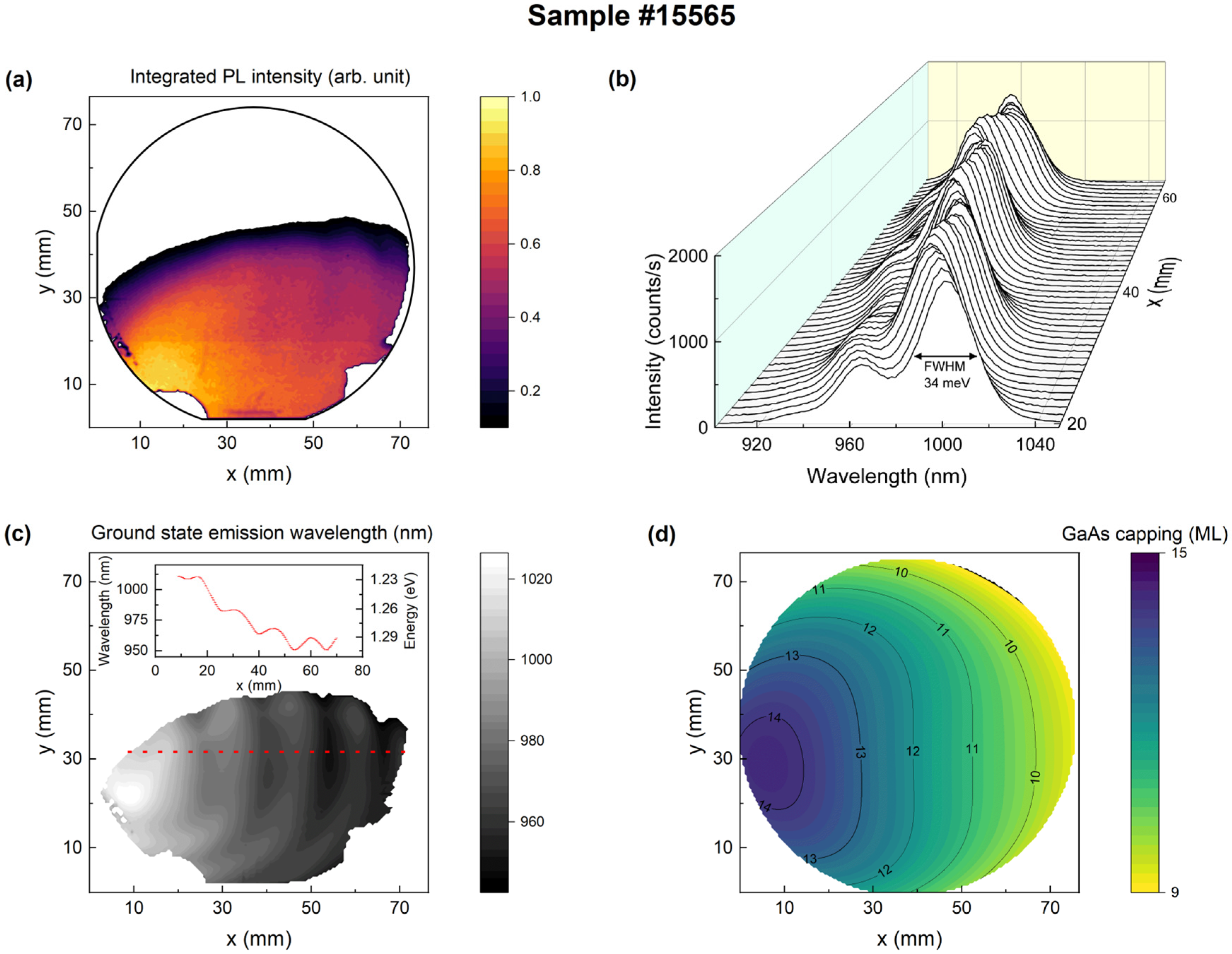
Figure 3.
Schematic representation of the overgrowth and anneal process for a rough and a smooth surface. (a) A QD typical for our growth parameters. (b) The QD is overgrown with a few ML GaAs. GaAs cannot grow on the QD because of the high strain. Ga and In atoms migrate away from the top of the QD and form a wall around it. The height of the QD is greatly reduced during this process. (c) The growth of the capping layer is completed. The effects of segregation of In from the wetting layer, diffusion of the InGaAs wall around the QD, and sublimation of In are shown for a rough surface (left) and for a smooth surface (right). On the left side, half a monolayer of more GaAs was grown. (d) The temperature rapidly increased according to the indium flush method. The ring around the QD has diffused away. The QD surrounded by a rough surface before annealing has a higher indium content in its interior and immediate surroundings.
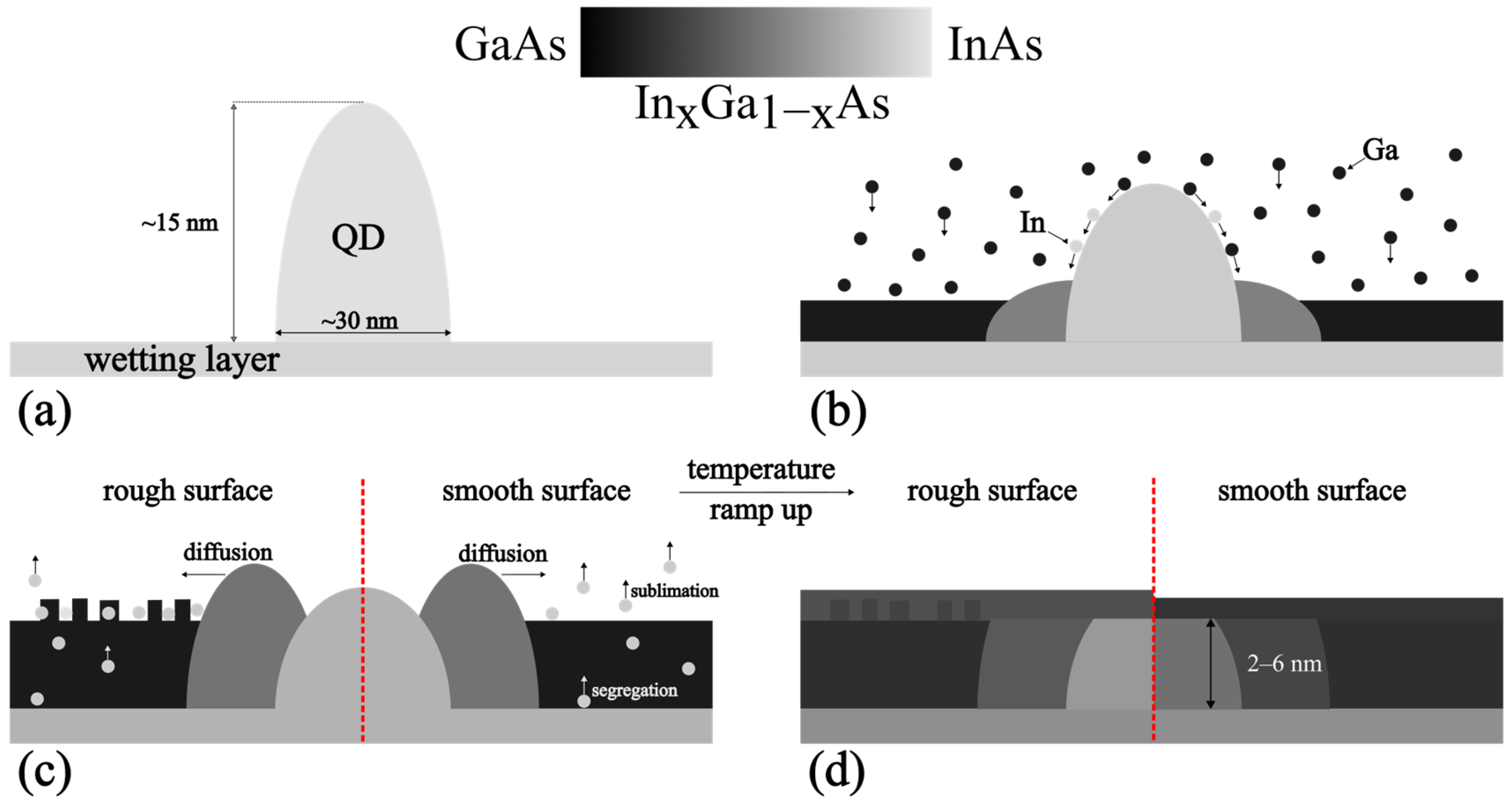
Figure 4.
PL measurements of sample #15633 with a flushing gradient from 10 to 6 ML. (a) The wafer map displays the ground state QD emission wavelength, which was extracted through Gaussian fitting of the PL data. (b) A waterfall plot showing the PL spectra taken at the gradient along y = 33 mm marked with a dashed line in (a). (c) The ground state emission wavelength and energy along the dashed line in (a). (d) Growth rate simulation of the GaAs capping thickness on the wafer.
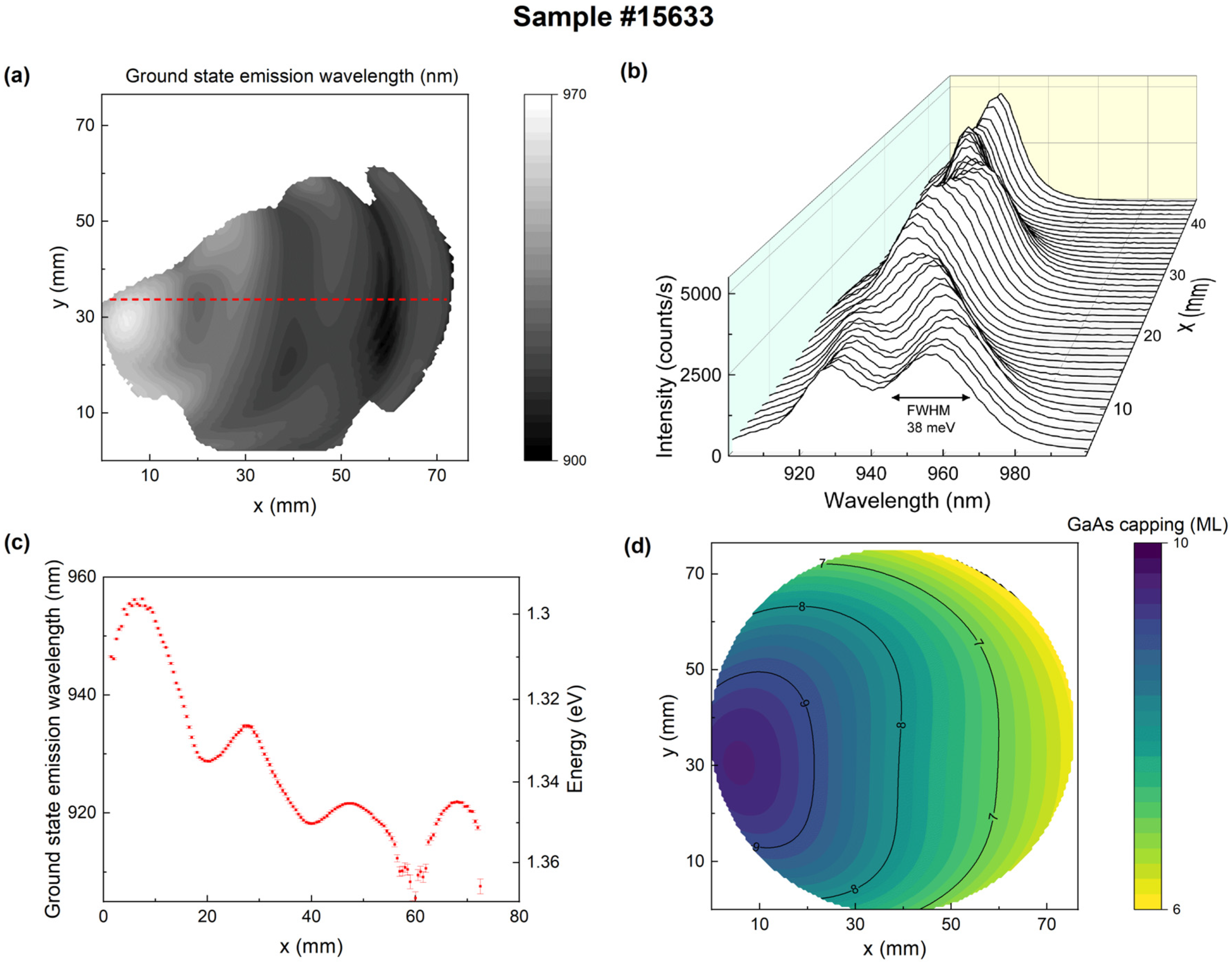
Figure 5.
The ground state emission energies of three samples along the gradients marked in red were plotted against the simulated GaAs capping layer.
Figure 5.
The ground state emission energies of three samples along the gradients marked in red were plotted against the simulated GaAs capping layer.
Disclaimer/Publisher’s Note: The statements, opinions and data contained in all publications are solely those of the individual author(s) and contributor(s) and not of MDPI and/or the editor(s). MDPI and/or the editor(s) disclaim responsibility for any injury to people or property resulting from any ideas, methods, instructions or products referred to in the content. |
© 2023 by the authors. Licensee MDPI, Basel, Switzerland. This article is an open access article distributed under the terms and conditions of the Creative Commons Attribution (CC BY) license (https://creativecommons.org/licenses/by/4.0/).
Share and Cite
MDPI and ACS Style
Spitzer, N.; Bart, N.; Babin, H.-G.; Schmidt, M.; Wieck, A.D.; Ludwig, A. Wafer-Scale Emission Energy Modulation of Indium Flushed Quantum Dots. Crystals 2023, 13, 1657. https://doi.org/10.3390/cryst13121657
AMA Style
Spitzer N, Bart N, Babin H-G, Schmidt M, Wieck AD, Ludwig A. Wafer-Scale Emission Energy Modulation of Indium Flushed Quantum Dots. Crystals. 2023; 13(12):1657. https://doi.org/10.3390/cryst13121657
Chicago/Turabian StyleSpitzer, Nikolai, Nikolai Bart, Hans-Georg Babin, Marcel Schmidt, Andreas D. Wieck, and Arne Ludwig. 2023. "Wafer-Scale Emission Energy Modulation of Indium Flushed Quantum Dots" Crystals 13, no. 12: 1657. https://doi.org/10.3390/cryst13121657
Note that from the first issue of 2016, this journal uses article numbers instead of page numbers. See further details here.