
An Alternative to Chlorobenzene as a Hole Transport Materials Solvent for High-Performance Perovskite Solar Cells
by

Seung Ho Lee
1,†,
Seong Bin Lim
2,†,
Jin Young Kim
1,
Seri Lee
2,
Se Young Oh
2,* and
Gyu Min Kim
1,* 1
Faculty of Food Biotechnology and Chemical Engineering, Hankyong National University, Anseong 17579, Republic of Korea
2
Department of Chemical and Biomolecular Engineering, Sogang University, Seoul 04107, Republic of Korea
*
Authors to whom correspondence should be addressed.
†
These authors contributed equally to this work.
Crystals 2023, 13(12), 1667; https://doi.org/10.3390/cryst13121667
Submission received: 12 November 2023
/
Revised: 2 December 2023
/
Accepted: 5 December 2023
/
Published: 7 December 2023
(This article belongs to the Special Issue Effect of Solvents and Solution Chemistry on the Properties of Perovskite Solar Cells)
Abstract
:Spiro-OMeTAD is a widely used hole-transporting layer (HTL) material, characterized by high hole mobility and good film-forming properties, in perovskite solar cells (PSCs). However, this material has high synthesis costs, low solubility, dependence on hygroscopic dopants, and a low commercial potential. Recently, we investigated alternative materials with good solubility, simple synthetic methods, and good electrical characteristics for use as hole transport materials (HTM) in triple-cation PSCs. Herein, (E,E,E,E)-4,4′,4″,4′″-[Benzene-1,2,4,5-tetrayltetrakis(ethene-2,1-diyl)]tetrakis[N,N-bis(4-methoxyphenyl)aniline], which has a small molecular weight and similar properties to Spiro-OMeTAD, was assessed for use as a HTM via a pre-test of device performance, including its electrical properties, surface morphology, and coating process method, with PSC efficiencies routinely surpassing 20%. A remarkable open-circuit voltage of 1.111, along with a photovoltaic efficiency of 20.18% was obtained in PSCs using this HTM with dichloromethane (DCM) instead of chlorobenzene, indicative of its potential for the fabrication of resistance components with improved surface uniformity. These results provide insights into DCM as an efficient solvent for small molecule-based HTM.
1. Introduction
The generation of energy from solar cells is highly regarded as a potential source of renewable energy because of the low costs associated with its distributed power generation, operation, and maintenance [1]. Over the years, PSCs based on organic–inorganic halide materials have attracted significant interest as a low-cost and high-power conversion-efficiency photovoltaic technology, achieving efficiencies as high as 26.08% [2].
Recently, PSCs have also gained research attention for their potential to remove barriers to perovskite commercialization. Hence, a multitude of researchers are currently deeply engrossed in the advancement of PSCs, dedicating their efforts to designing innovative device architectures, exploring nanostructures, refining synthesis methods, and tweaking chemical compositions. Their overarching goal is to meticulously optimize the properties of thin-film layers [3,4,5,6,7,8]. Moreover, there is a concerted effort to unravel the intricate effects of doping on the performance, stability, and advancement of various deposition processes used for crafting high-quality perovskite films and coated layers, a pursuit that is being pursued with vigor and dedication [9,10,11,12,13]. In the intricate realm of PSC manufacturing, the primary deposition techniques employed for constructing top-tier thin films are the universal vapor- and solution-based deposition methods. These methodologies play a pivotal role in shaping the structural integrity and functional characteristics of PSCs, contributing to their overall efficiency and performance.
Conventional photovoltaic operations necessitate precise band-edge alignment, imposing significant constraints on the range of hole and electron-transporting materials viable for use in PSCs. Notably, 2,2′,7,7′-Tetrakis[N,N-di(4-methoxyphenyl)amino]-9,9′-spirobifluorene (Spiro-OMeTAD) has emerged as the go-to HTM in PSCs configured with n-i-p structures, owing to its exceptional performance [14,15,16,17,18,19]. This widespread usage attests to its effectiveness in facilitating efficient charge transport within the solar cell architecture, a critical aspect for achieving optimal photovoltaic performance. Although PSCs with Spiro-OMeTAD are unstable at high temperatures (60–120 °C), they are considered an important HTM for the fabrication of n-i-p PSCs compared to other HTMs in terms of efficiency. Spiro-OMeTAD is a prominent HTM in standard PSCs because of its high solubility, film formability, proper ionization potential, matched absorption spectrum, and uniformly smooth solid-state morphology [17]. However, the unaltered Spiro-OMeTAD solution inherently lacks the requisite mobility and conductivity necessary for the efficient conveyance of photogenerated holes, primarily due to the unwieldy tridimensional nature of its molecules. This inherent limitation culminates in devices characterized by elevated series resistance and diminished overall performance. While various strategies have been devised to ameliorate this issue, they entail additional processing steps during device fabrication, which introduce complexities that compromise both economic efficiency and procedural simplicity [18,19]. Conversely, the exploration of optimizing commercially viable, cost-effective processes by leveraging solvents and adopting comparable chemical structures has garnered attention across numerous research groups. These endeavors have not only showcased effectiveness but also unveiled the potential for a more streamlined and straightforward approach [20,21,22,23].
In this study, our primary focus is on elucidating the meticulous control of thin-film morphology and the optimization of charge transport within PSCs. We employ alternative materials and solvents possessing properties akin to Spiro-OMeTAD, aiming to curtail costs without compromising on performance equivalence. Within the scope of this research, we present a detailed exploration of the performance outcomes of PSCs engineered with the integration of a cathode interlayer. This strategic approach not only seeks to enhance the cost-effectiveness of PSC fabrication but also underscores the importance of achieving a performance level on par with conventional materials. Notably, the properties of HTM and solvents in PSCs, namely (E,E,E,E)-4,4′,4″,4′″-[Benzene-1,2,4,5-tetrayltetrakis(ethene-2,1-diyl)]tetrakis[N,N-bis(4-methoxyphenyl)aniline] (TOP-HTM-α2) and dichloromethane (DCM), respectively, exhibited an excellent hole mobility and surface morphology, as well as a cheaper alternative to Spiro-OMeTAD. By controlling the amount of TOP-HTM-α2 in commonly used chlorobenzene (CB) and newly introduced DCM, a HTL can be created at the top surface of the perovskite film that optimizes the active layer and mitigates problems associated with electrode interface contact [24,25].
To this end, the performance of the PSCs was compared to that of devices with Spiro-OMeTAD and TOP-HTM-α2 as HTMs under DCM and CB solvent conditions. The hole transport layer was generated via simple and conventional methods without an annealing process under ambient conditions. The roughness of the surfaces implied that the top of the perovskite active layer could be covered using the large optimum thickness of the TOP-HTM-α2 layer rather than the Spiro-OMeTAD layer. This indicates that the use of TOP-HTM-α2 (in DCM) as the HTL is beneficial as it decreases the contact resistance between the active layer and the electrode. The electrical and major surface characteristics of HTM were measured using a fabricated hole-only device, X-ray diffraction (XRD), and atomic force microscopy (AFM). The performance of PSCs with a TOP-HTM-α2 (in DCM) layer is discussed herein, with a particular focus on alternative HTMs of spiro-OMeTAD, low-cost fabrication, and excellent mobility.
2. Materials and Methods
2.1. Materials
N,N-dimethylformamide (DMF, 99.5%), N-methylpyrrolidone (NMP, 99.0%), CB (99.8%), DCM (99.0%), and TOP-HTM-α2 (98.0%) were purchased from TCI Chemicals (Tokyo, Japan). Cesium bromide (CsBr, 99.9%), lead (II) iodide (PbI2, 99.99%), formamidine iodide (FAI, 99.0%), Spiro-OMeTAD (99.0%), lithium bis(trifluoromethylsulfonyl) imide (Li-TFSI, 99.99%), 4-tert butylpyridine (tBP, 98.0%), and methylammonium chloride (MACl, 99.0%) were purchased from Sigma-Aldrich (St. Louis, MI, USA). Tin oxide (SnO2, 15% in an H2O colloidal dispersion liquid) and 3-(formamidinothio)-1-propanesulfonic acid (FTPS) were purchased from Alfa (Ward Hill, Massachusetts, USA). All materials were used as received without further purification.
2.2. Preparation of Precursors
The SnO2 solutions were diluted to four times the volume of the FTPS solutions (0.3 mg/mL) [26]. The perovskite precursor solution was prepared from a DMF/NMP co-solvent (9:1 volume ratio) containing PbI2 (1.35 M), FAI (1.0 M), CsBr (0.2 M), and MACl (0.2 M). The composition of perovskite was (FA)0.85(CS)0.15(Br)0.15(Pb)1(I)2.85(MA)0.15. Spiro-OMeTAD (0.059 M) was dissolved in CB using Li-TFSI and tBP as additives. The molar ratio of Spiro-OMeTAD:Li-TFSI:tBP was 1:0.53:3.33. TOP-HTM-α2 (0.028 M) was dissolved in DCM with Li-TFSI and tBP as additives. The molar ratio of TOP-HTM-α2:Li-TFSI:tBP was 1:0.78:4.52.
2.3. Device Fabrication
The ITO glass substrates with a patterned design underwent a thorough cleaning process in an ultrasonic bath containing a 2% Hellmanex detergent, deionized water, acetone, and isopropyl alcohol. Each cleaning step lasted for 15 min, culminating in ultraviolet/ozone treatment for an additional 6 min. The detailed device structure and energy level of materials were visually represented in Figure 1a,b. The structure of the PSCs comprised layers in the sequence of ITO/SnO2/perovskite/HTM (Spiro-OMeTAD or TOP-HTM-α2)/Au. A SnO2 solution (100 μL) was spin coated onto the ITO substrate, subjected to spinning at 5000 rpm for 30 s, and subsequently annealed at 150 °C for 25 min. This step was followed by an additional ultraviolet/ozone treatment lasting 6 min. The perovskite precursor (50 μL) was spin coated onto the SnO2-coated substrate at 3000 rpm for 30 s. During the spin-coating process, 20 μL of CB was dripped as an antisolvent 15 s before the spin-coating concluded. The resulting film underwent annealing at 120 °C for 60 min. The HTM precursor (50 μL)—either Spiro-OMeTAD or TOP-HTM-α2—was spin coated onto the perovskite films at 2500 rpm for 30 s. Following this, a 100 nm thick layer of Au was thermally evaporated using the KVE-T2000 equipment (Korea Vacuum Tech, Gimpo-si, Republic of Korea). Notably, the entire PSCs fabrication process, including the coating of perovskite and the HTL, was conducted in a dry air environment with humidity levels maintained below 20%. A visual representation of the PSCs fabrication process is outlined in Figure S1.
2.4. Measurements and Characterizations
The investigation into the characteristics of the current density voltage (J-V) was meticulously conducted under simulated conditions, employing 1 sun illumination (equivalent to 100 mW/cm2 AM 1.5 G). This assessment was carried out using a sophisticated solar cell I-V test system (T2003; Ossila, Sheffield, UK) complemented by a solar simulator lamp (LSH-7320; Newport, RI, USA) to ensure precise and controlled experimental conditions. External quantum efficiency (EQE) measurements were executed using the advanced K3100 instrument (McScience, Suwon-si, Republic of Korea), which played a pivotal role in providing a comprehensive understanding of the efficiency of the solar cell across different wavelengths. This analytical approach contributes valuable insights into the performance of the PSCs under consideration. To evaluate the morphological aspects of the HTL, AFM was employed for detailed detection and characterization. The utilization of AFM, specifically the MFP-3D Origin+ model by Oxford Instruments (Abingdon, UK), enabled a high-resolution analysis of the surface morphology, shedding light on the structural intricacies of the HTL. For a more comprehensive understanding of the PSC structure, cross-sectional scanning electron microscopy (SEM) images were obtained. The utilization of a field-emission SEM (JSM-710F; JEOL Co., Ltd., Tokyo, Japan) allowed for detailed visualizations, enabling the examination of the layer-by-layer composition and structural integrity of the PSCs. Furthermore, XRD analysis using the SmartLab instrument by Rigaku (Tokyo, Japan) was employed to characterize the crystallographic structure of the samples. This analytical technique provides essential information about the crystalline phases present in the perovskite films, offering crucial insights into the material properties and quality. In essence, the comprehensive characterization of the samples through a range of advanced analytical techniques ensures a thorough exploration of the structural, morphological, and crystallographic aspects, contributing to a holistic understanding of the PSCs under study.
3. Results
3.1. Device Characterization
In the present study, we strategically employed TOP-HTM-α2 as an alternative material in lieu of the conventionally utilized Spiro-OMeTAD. To assess its compatibility and performance, we conducted comprehensive solubility experiments that aimed to discern the most suitable solvent, compare the device performance under various solvent conditions, and juxtapose the outcomes with a control group. The outcomes of these experiments unequivocally demonstrate that the integration of TOP-HTM-α2 leads to a noteworthy enhancement in device performance. Our findings unveil a straightforward and efficacious process that leverages a low boiling point and readily soluble solvent, a methodology derived from thorough analyses encompassing surface characteristics, dynamic behaviors, and electrical properties. In the context of dissolving TOP-HTM-α2 with CB, a solvent commonly employed for dissolving HTM, an interesting observation emerged. It was noted that TOP-HTM-α2 did not dissolve at room temperature, requiring elevated temperatures, specifically 90 °C, for complete dissolution. This intricacy highlights the need for optimization in the fabrication process of PSCs when utilizing CB as the solvent. This optimization endeavor becomes crucial to ensure the effective integration of TOP-HTM-α2 into the fabrication process, maximizing its potential benefits.
In Figure S2, the chemical structure of the solvent utilized in the initial experiments is presented. These preliminary experiments aimed to circumvent solution heating and annealing steps, focusing on identifying a solvent that exhibits solubility at room temperature. Simultaneously, Figure S3 visually depicts the appearance of TOP-HTM-α2 after dissolution in the selected solvent. The crucial observation from Figures S2 and S3 is the confirmation that a solvent capable of dissolving TOP-HTM-α2 at room temperature necessitates the presence of two or more R-Cl moieties while excluding a benzene structure. This strategic solvent selection is imperative for optimizing the dissolution process of TOP-HTM-α2 under ambient conditions, aligning with the objective of streamlining fabrication steps in the experimental procedure.
The J-V characteristics of PSCs using solvents are shown in Figure S4 and Table S1. There are differences in power conversion efficiency (PCE), open-circuit voltage (Voc), fill factor (FF), and short-circuit current density (Jsc) depending on each solvent. It was confirmed that the use of DCM as a solvent provided the highest performance. DCM is evaporated rapidly during the spin-coating without an annealing step due to its low boiling point, and TOP-HTM-α2 will move upward together with DCM and finally reach the top surface to form a uniform surface to TOP-HTM-α2-rich layer [27]. DCM exhibits better solubility in TOP-HTM-α2 compared to CB, and its lower boiling point results in shorter contact time with the perovskite layer in the liquid state. The shorter the contact time, the less influence the solvent has on the perovskite. Therefore, using a solvent with a low boiling point can have a positive effect by reducing the contact time with the perovskite layer. The corresponding J-V curves of the PSCs are visually depicted in Figure 2a. This graphical representation serves as a comprehensive illustration of the cells’ electrical characteristics under varying operational conditions. To delve deeper into the performance metrics of these solar cells, namely, Jsc, Voc, FF, and PCE, a detailed summary is provided in Table 1. This tabular presentation offers a succinct yet informative overview of the key parameters governing the effectiveness and efficiency of fabricated solar cells. According to the results, the PCE of the reference device with Spiro-OMeTAD (in CB) as HTM was 18.85%, with a Jsc of 23.42 mA/cm2, Voc of 1.086 V, and FF of 75.06%. When using HTM as TOP-HTM-α2 with DCM, the PCE value was 20.18% with a Jsc of 23.58 mA/cm2, a Voc of 1.111 V, and an FF of 76.97%. However, in the case of CB, the cell performance worsened as discussed previously, due to the very poor solubility of TOP-HTM- α2 in CB. Using TOP-HTM-α2, the PCE value of PSCs increased, which is indicative of dependence on the solvent.
The EQE curves of the best-performing devices are presented in Figure 2b. From there, it can be inferred that a high value of ~90% was obtained in the wavelength between 350 and 450 nm, which could be explained by a decrease in absorption by HTL when a TOP-HTM-α2 was implemented in comparison to Spiro-OMeTAD. The observed increment in EQE can be attributed to the noteworthy impact of transitioning from CB to DCM as the solvent. The distinct characteristics of the J-V and EQE curves underscore a discernible influence of the solvent on the performance of the HTM within the device. Specifically, TOP-HTM-α2 demonstrated optimal conditions when dissolved in DCM, showcasing superior performance, while Spiro-OMeTAD exhibited peak performance when dissolved in CB. This stark contrast in the choice of solvent highlights the nuanced relationship between the HTM and the solvent, emphasizing the critical role of solvent selection in tailoring and optimizing the performance of PSCs.
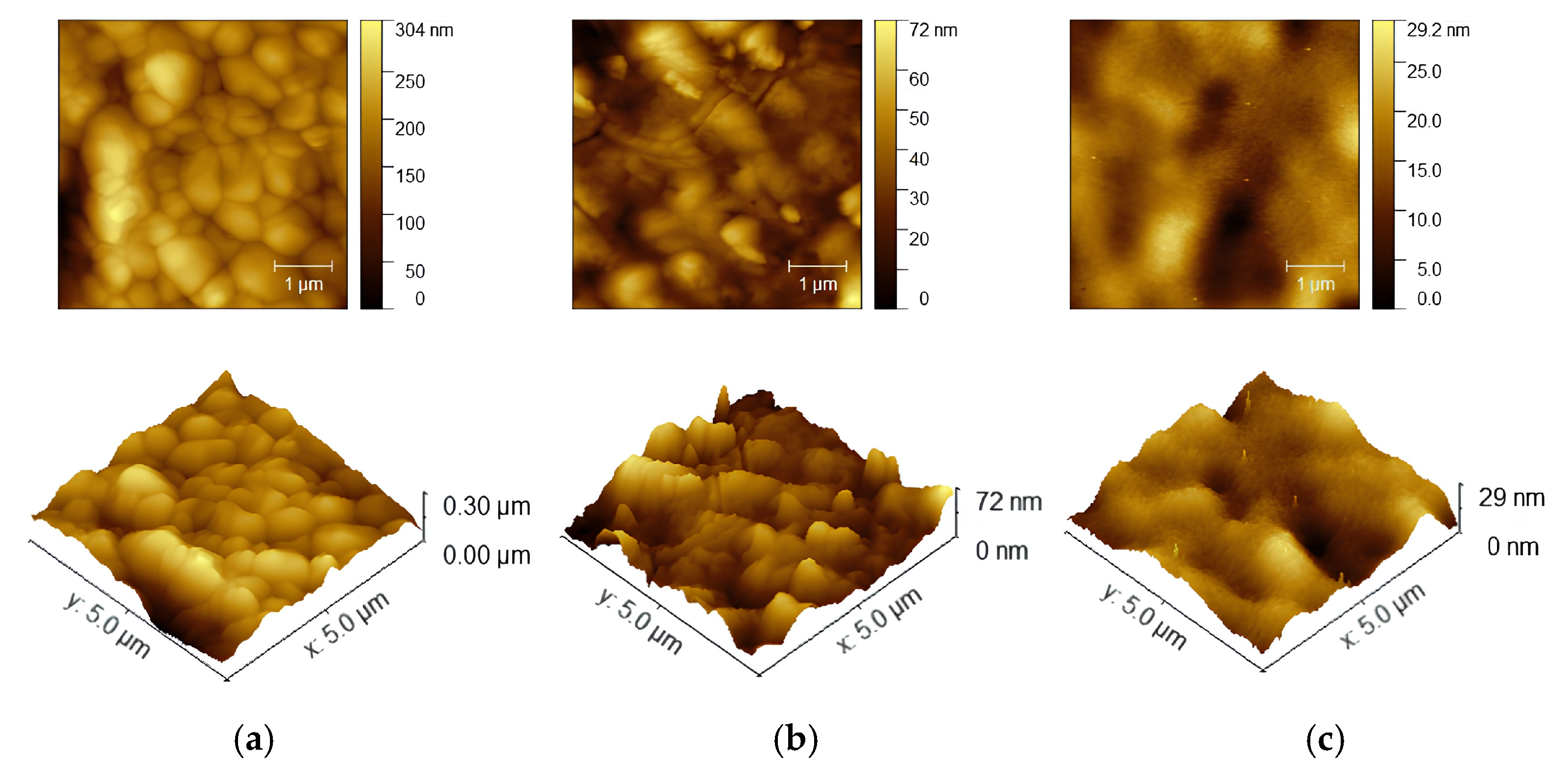
3.2. Surface Analysis
The corresponding morphology and roughness were subjected to further in-depth analysis using AFM, as illustrated in Figure 3. AFM examination was conducted employing tapping mode with a 5 μm × 5 μm image size. The film based on Spiro-OMeTAD (in CB) displayed a noticeably uneven surface, characterized by its roughness. In contrast, the film based on TOP-HTM-α2 exhibited a more uniform and smoother surface. Specifically, the TOP-HTM-α2-based film showcased a significantly lower Root Mean Square Roughness (Rrms) of 4.41 nm, a notable improvement compared to the Spiro-OMeTAD (in CB)-based film with an Rrms of 11.26 nm. The observed roughness on the surfaces suggests that the triple-cation perovskite films can achieve better coverage when employing the substantial optimum thickness of the TOP-HTM-α2-based film (in DCM) compared to the Spiro-OMeTAD film (in CB). This disparity in roughness further underscores the strategic advantage of using TOP-HTM-α2, particularly in conjunction with dichloromethane, for achieving superior film coverage and surface quality in the fabrication of perovskite films. The analysis of EQE and AFM results emphasized the favorable attributes of DCM as the solvent for TOP-HTM-α2. The rationale behind designating DCM as the optimal choice lies in its correlation with an increased current density value. The application of TOP-HTM-α2 in conjunction with DCM not only yields a heightened current density but also facilitates the formation of a surface characterized by uniformity and smoothness. This uniform surface holds strategic significance as it actively contributes to the mitigation of contact resistance between the electrode and the perovskite layer. The consequential reduction in contact resistance is particularly noteworthy in enhancing the overall efficiency and performance of the device. Moreover, the observed uniformity in the surface texture appears to play a direct role in influencing the series resistance, as highlighted in the prior literature [28].
In essence, the meticulous choice of DCM as the solvent in the TOP-HTM-α2 application process emerges as a decisive factor in optimizing both the electrical and surface characteristics, leading to a more efficient and effective integration of these advanced materials into the perovskite film. The HTL surface layer was analyzed in the absence of annealing, and as a result, the results were confirmed to be related to AFM. Upon employing TOP-HTM-α2 as the HTL, a discernibly smoother surface was observed. This enhanced surface quality was complemented by a measured thickness of 500 ± 20 nm for the perovskite film, as revealed by cross-sectional imaging in Figure 4 using SEM. The strategic choice of utilizing a TOP-HTM-α2-based film (in DCM) as the HTL proves to be advantageous, primarily attributed to its capability to mitigate the contact resistance between the triple-cation perovskite films and the electrode, as emphasized in previous studies [29]. This reduction in contact resistance not only contributes to the aesthetic improvement of the film’s surface but also plays a pivotal role in fostering more efficient and reliable interactions between the perovskite layer and the electrode. The resulting enhancement in contact efficiency holds promising implications for elevating the overall performance and efficiency of devices that incorporate these cutting-edge materials.
3.3. Materials Properties as HTL
A comparison of the XRD patterns of triple-cation perovskite films on glass substrates is provided in Figure 5. Diffraction peaks were observed at 14.1°, 20.0°, 24.5°, 28.3°, 31.8°, 35.1°, 40.5°, and 43.1°, which are attributed to the (110), (112), (202), (220), (310), (312), (224), and (314) diffraction planes of the octahedral Immm space group. The crystallization conditions of the triple-cation perovskite films were unchanged after coating with HTM (Spiro-OMeTAD or TOP-HTM-α2) [30].
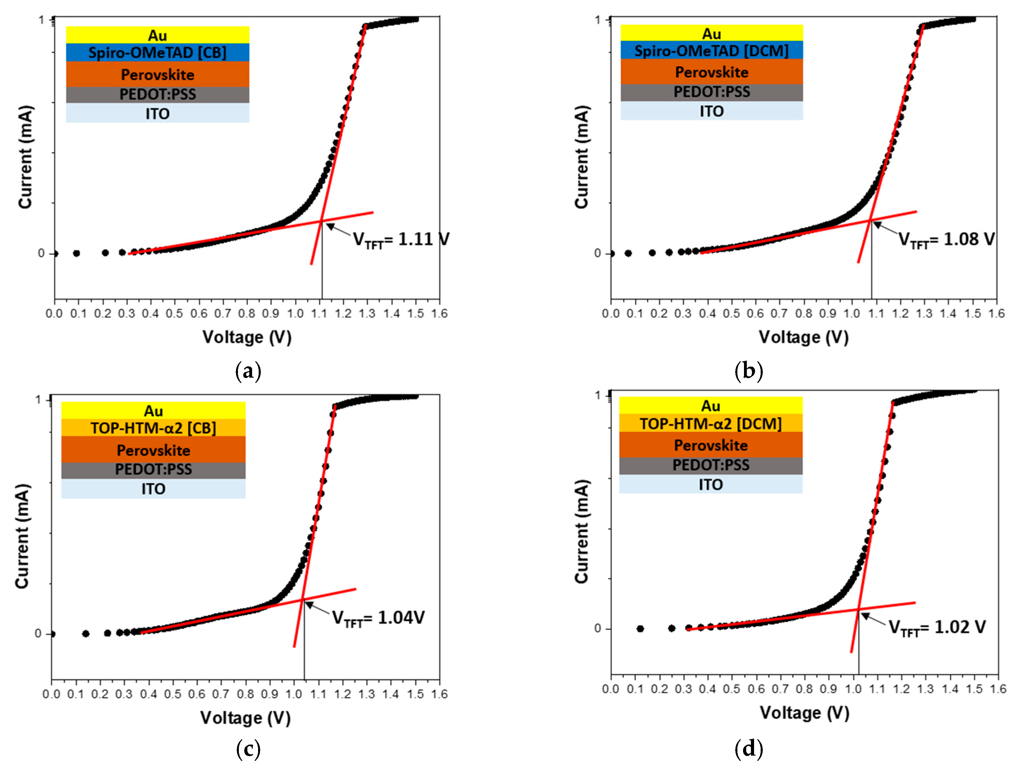
In this study, given the singular utilization of one type of perovskite, the characteristics of carrier mobility are anticipated to be primarily influenced by the properties of the Charge Transport Layer (CTL). In order to elucidate the specific attributes of the HTL under the influence of various solvents, we conducted tests to observe either hole mobility or trap density existing between the perovskite layer and the HTL [31]. As depicted in Figure 6, the capacitance–voltage (C-V) curves exhibited distinct regions, including the ohmic region, trap-filling-limited region, and space-charge-limited current. The ohmic response and trap-filling phenomena were particularly noteworthy as the voltage increased continuously, potentially leading to the termination of a linear J-V relation. These observations provide valuable insights into the charge transport dynamics at the interface of the perovskite layer and the HTL, shedding light on the nuanced interactions governing the device’s performance. For the hole-only device, a trap-filling-limited voltage (VTFL) of 1.11 V for Spiro-OMeTAD with a CB device and a 1.02 V trap-filling limited-voltage for TOP-HTM-α2 with a DCM device was measured. The trap state density was calculated using Equation (1):
where L is the thickness of the perovskite layer, ε is the dielectric constant, ε0 is the vacuum dielectric constant, and q is the elementary charge. VTFL of TOP-HTM-α2 with a DCM device was 1.02 V, lower than that of the Spiro-OMeTAD (in CB)-based film device [32,33]. Significantly, the data obtained through space-charge-limited current (SCLC) measurements in this study places a distinct emphasis on measuring trap-filled-limited voltage rather than focusing solely on hole mobility. The analytical approach was strategically designed to ascertain the quantity of hole traps present between the perovskite layer and different HTLs [34,35]. This subtlety analysis provides a deeper understanding of the charge transport dynamics and the impact of various HTLs on the VTFL in the PSCs structure.
Through an exhaustive series of device fabrication processes and thorough analyses, we meticulously confirmed that the utilization of DCM resulted in enhanced efficiency and a reduction in the fabrication process time in comparison to Spiro-OMeTAD. The solar simulator results from the iterative experiments are visually represented in Figure S5, and additional data can be found in Table S2.
4. Conclusions
The results presented in this study demonstrate that alternative materials (TOP-HTM-α2) and a solvent with similar properties to Spiro-OMeTAD can be used to control thin-film morphology and the optimization of charge transport in PSCs in order to improve the cost-effectiveness and generate an equivalent performance. The J-V characteristics of the devices showed that the absorption layer with triple-cation perovskite structure and electrode interface contact problems were optimized compared with those of the controlled materials for HTL, thus resulting in an increase in PCE. AFM and XRD measurements confirmed that the electrical and major surface characteristics of HTM implied that the top of the perovskite active layer can achieve a better coverage via the use of the large optimum thickness of the TOP-HTM-α2 layer rather than the Spiro-OMeTAD layer. Furthermore, the TOP-HTM-α2-based film exhibited a lower Rrms (4.41 nm) compared with the Spiro-OMeTAD (in CB)-based film (11.26 nm). These findings suggest that the low-boiling solvent (DCM in this study) processing method use of TOP-HTM-α2 can be an effective approach compared to CB-based solvent to decrease the contact resistance between the active layer and electrode, which is of great importance for the optimization of low-cost processes of PSCs in practical applications. The majority of non-polar solvents, including DMF, CB, dichlorobenzene (DCB), and toluene, which are all commonly employed as universal solvents in the PSCs fabrication process, are typically associated with high-temperature procedures. However, to enhance stability and mitigate risks in practical industrial applications, there is a distinct advantage in transitioning to low-temperature processes. Our ongoing research is centered on realizing low-temperature methodologies for materials that can substitute and enhance existing components within the PSCs fabrication process. The ultimate objective is to enable the entire device fabrication process to be conducted at temperatures below 100 °C, aligning with industry benefits for improved efficiency and operational feasibility.
Supplementary Materials
The following supporting information can be downloaded at: https://www.mdpi.com/article/10.3390/cryst13121667/s1, Figure S1. PSCs fabrication process; Figure S2. Chemical structure of the solvent; Figure S3. Appearance of TOP-HTM-α2 after dissolving the solvent; Figure S4. J-V characteristic of PSCs using TOP-HTM-α2 with differnet solvents; Figure S5. Box plot: (a) PCE, (b) Voc, (c) FF, and (d) Jsc for PSCs; Table S1. Summary of detailed performance parameters of PSCs; Table S2. Summary of detailed performance parameters of PSCs.
Author Contributions
Conceptualization, S.H.L. and S.B.L.; methodology, S.H.L. and S.B.L.; software, S.H.L. and S.B.L.; validation, S.H.L. and S.B.L.; formal analysis, S.H.L., S.B.L., J.Y.K. and S.L.; investigation, S.H.L. and S.B.L.; resources, S.H.L. and S.B.L.; data curation, S.H.L. and S.B.L.; writing—original draft preparation, S.H.L. and S.B.L.; writing—review and editing, G.M.K.; visualization, S.H.L. and S.B.L.; supervision, G.M.K. and S.Y.O.; project administration, G.M.K.; funding acquisition, G.M.K. All authors have read and agreed to the published version of the manuscript.
Funding
This work was supported by a research grant from Hankyong National University in the year of 2021.
Data Availability Statement
The data collected in this study are presented and available in this article.
Conflicts of Interest
The authors declare no conflict of interest.
References
- Mosher, D.; Boese, R.; Soukup, R. Advantages of Sun tracking for planar silicon solar cells. Sol. Energy 1977, 19, 91–97. [Google Scholar] [CrossRef]
- Park, J.; Kim, J.; Yun, H.; Paik, M.J.; Noh, E.; Mun, H.J.; Kim, M.G.; Shin, T.J.; Seok, S.I. Controlled growth of perovskite layers with volatile alkylammonium chlorides. Nature 2023, 616, 724–730. [Google Scholar] [CrossRef] [PubMed]
- Rong, Y.; Hu, Y.; Mei, A.; Tan, H.; Saidaminov, M.I.; Seok, S.I.; McGehee, M.D.; Sargent, E.H.; Han, H. Challenges for Commercializing Perovskite Solar Cells. Science 2018, 361, 1214. [Google Scholar] [CrossRef] [PubMed]
- Falaras, C.; Stathatos, E. Performance Enhancement and Stability Improvement in Perovskite Solar Cells via Interface Functionalization. Electronics 2023, 12, 3319. [Google Scholar] [CrossRef]
- Jiang, Q.; Song, Z.; Bramante, R.C.; Ndione, P.F.; Tirawat, R.; Berry, J.J.; Yan, Y.; Zhu, K. Highly efficient bifacial single-junction perovskite solar cells. Joule 2023, 7, 1543–1555. [Google Scholar] [CrossRef]
- Yelzhanova, Z.; Nigmetova, G.; Aidarkhanov, D.; Daniyar, B.; Baptayev, B.; Balanay, M.P.; Junmabekov, A.N.; Ng, A. A Morphological Study of Solvothermally Grown SnO2 Nanostructures for Application in Perovskite Solar Cells. Nanomaterials 2022, 12, 1686. [Google Scholar] [CrossRef] [PubMed]
- Huang, D.; Xiang, H.; Ran, R.; Wang, W.; Zhou, W.; Shao, Z. Recent Advances in Nanostructured Inorganic Hole-Transporting Materials for Perovskite Solar Cells. Nanomaterials 2022, 12, 2592. [Google Scholar] [CrossRef]
- Zhu, C.; Wang, X.; Li, H.; Wang, C.; Gao, Z.; Zhang, P.; Niu, X.; Li, N.; Xu, Z.; Su, Z.; et al. Stress compensation based on interfacial nanostructures for stable perovskite solar cells. Interdiscip. Mater. 2023, 2, 348–359. [Google Scholar] [CrossRef]
- Gu, Y.; Wang, H.; Sun, J.; Lu, Y.; Luo, P.; Hu, J. Fabrication of efficient and stable wide band gap CsPbIBr2 inorganic perovskite solar cells via doping with lead chloride compound. J. Alloys Compd. 2023, 963, 171291. [Google Scholar] [CrossRef]
- Guo, Y.; Chen, W.; Wang, H.; Cai, W.; Qaid, S.M.H.; Zang, Z. Additive Conformational Engineering to Improve the PbI2 Framework for Efficient and stable Perovskite Solar Cells. Inorg. Chem. 2023, 62, 14086–14093. [Google Scholar] [CrossRef]
- Lee, S.U.; Park, H.; Shin, H.; Park, N.G. Atomic layer deposition of SnO2 using hydrogen peroxide improves the efficiency and stability of perovskite solar cells. Nanoscale 2023, 15, 5044–5052. [Google Scholar] [CrossRef] [PubMed]
- Yang, Y.; Zhang, Y.; Li, R.; Mbumba, M.T.; Akram, M.W.; Pan, J.; Cai, M.; Dai, S.; Guli, M. Low-Temperature Atomic Layer Deposition of Double-Layer Water Vapor Barrier for High Humidity Stable Perovskite Solar Cells. Adv. Opt. Mater. 2023, 11, 202300148. [Google Scholar] [CrossRef]
- Teixeira, C.; Fuentes-Pineda, R.; Andrade, L.; Mendes, A.; Forgacs, D. Fabrication or low-cost and flexible perovskite solar cells by slot-die coating for indoor applications. Mater. Adv. 2023, 4, 3863–3873. [Google Scholar] [CrossRef]
- Kim, H.S.; Lee, C.R.; Im, J.H.; Lee, K.B.; Moehl, T.; Marchioro, A.; Moon, S.J.; Humphry-Baker, R.; Yum, J.H.; Moser, J.E.; et al. Lead Iodide Perovskite Sensitized All-Solid-State Submicron Thin Film Mesoscopic Solar Cell with Efficiency Exceeding 9%. Sci. Rep. 2012, 2, 591. [Google Scholar] [CrossRef]
- Lee, M.M.; Teuscher, J.; Miyasaka, T.; Murakami, T.N.; Snaith, H.J. Efficient Hybrid Solar Cells Based on Meso-Superstructured Organometal Halide Perovskites. Science 2012, 338, 643. [Google Scholar] [CrossRef]
- Ganesan, R.; Fu, K.; Gao, P.; Raabe, I.; Schenk, K.; Scopelliti, R.; Luo, J.; Wong, L.H.; Gratzel, M.; Nazzeruddin, M.K. A simple spiro-type hole transporting material for efficient perovskite solar cells. Energy Environ. Sci. 2015, 8, 1986–1991. [Google Scholar] [CrossRef]
- Hawash, Z.; Ono, L.K.; Qi, Y. Recent Advances in Spiro-MeOTAD Hole Transport Material and Its Application in Organic-Inorganic Halide Perovskite Solar Cells. Adv. Mater. Interfaces 2018, 5, 1700623. [Google Scholar] [CrossRef]
- Shen, Y.; Deng, K.; Li, L. Spiro-OMeTAD-Based Hole Transport Layer Engineering toward Stable Perovskite Solar Cells. Small Methods 2022, 6, 2200757. [Google Scholar] [CrossRef]
- Nakka, L.; Cheng, Y.; Aberle, A.G.; Lin, F. Analytical Review of Spiro-OMeTAD Hole Transport Materials: Paths Toward Stable and Efficient Perovskite Solar Cells. Adv. Energy Sustain. Res. 2022, 3, 2200045. [Google Scholar] [CrossRef]
- Ono, L.K.; Hawash, Z.; Jaarez-Perez, E.J.; Qiu, L.; Jiang, Y.; Qi, Y. The influence of secondary solvents on the morphology of a spiro-MeOTAD hole transport layer for lead halide perovskite solar cells. Appl. Phys. 2018, 51, 294001. [Google Scholar] [CrossRef]
- Hu, M.; Wu, X.; Tan, W.L.; Tan, B.; Scully, A.D.; Ding, L.; Zhou, C.; Xiong, Y.; Huang, F.; Simonov, A.N.; et al. Solvent Engineering of a Dopant-Free Spiro-OMeTAD Hole-Transport Layer for Centimeter-Scale Perovskite Solar Cells with High Efficiency and Thermal Stability. ACS Appl. Mater. Interfaces 2020, 12, 8260–8270. [Google Scholar] [CrossRef] [PubMed]
- Pham, H.D.; Wu, Z.; Ono, L.K.; Manzhosm, S.; Feron, K.; Motta, N.; Qi, Y.; Sonar, P. Low-Cost Alternative High-Performance Hole-Transport Material for Perovskite Solar Cells and Its Comparative Study with Conventional SPIRO-OMeTAD. Adv. Electron Mater. 2017, 3, 1700139. [Google Scholar] [CrossRef]
- Abdellah, I.M.; Chowdhury, T.H.; Lee, J.J.; Islam, A.; Nazzeruddin, M.K.; Graetzel, M.; El-Shafei, A. Facile and low-cost synthesis of a novel dopant-free hole transporting material that rivals Spiro-OMeTAD for high efficiency perovskite solar cells. Sustain. Energy Fuels 2021, 5, 199–211. [Google Scholar] [CrossRef]
- Nishimura, H.; Okada, I.; Tanabe, T.; Nakamura, T.; Murdey, R.; Wakamiya, A. Additive-Free, Cost-Effective Hole-Transporting Materials for Perovskite Solar Cells Based on Vinyl Triarylamines. ACS Appl. Mater. Interfaces 2020, 12, 32994–33003. [Google Scholar] [CrossRef] [PubMed]
- Kumar, A.; Singh, S.; Mohammed, M.K.A.; Ahmed, D.S. Experimental investigation of additive free-low-cost vinyl triarylamines based hole transport material for FAPbI3-based perovskite solar cells to enhance efficiency and stability. Mater. Res. Express 2023, 10, 044003. [Google Scholar] [CrossRef]
- Wang, C.; Wu, J.; Liu, X.; Wang, S.; Yan, Z.; Chen, L.; Li, G.; Zhang, X.; Sun, W.; Lan, Z. High-effective SnO2-based perovskite solar cells by multifunctional molecular additive engineering. J. Alloys Compd. 2021, 886, 161352. [Google Scholar] [CrossRef]
- Xiao, Y.; Zhou, S.; Su, Y.; Wang, H.; Ye, L.; Tsang, S.W.; Xie, F.; Xu, J. Enhanced efficiency of organic solar cells by mixed orthogonal solvents. Org. Electron. 2014, 15, 2007–2013. [Google Scholar] [CrossRef]
- Lim, S.B.; Ji, C.H.; Kim, K.T.; Oh, S.Y. Reduction of the Dark Current in a P3HT-Based Organic Photodiode with a Ytterbium-Fluoride Buffer Layer for Electron Transport. J. Korean Phys. Soc. 2016, 69, 421–425. [Google Scholar] [CrossRef]
- Chen, J.; Yang, Y.; Dong, H.; Li, J.; Zhu, X.; Xu, J.; Pan, F.; Yuan, F.; Dai, J.; Jiao, B.; et al. Highly efficient and stable perovskite solar cells enabled by low-dimensional perovskitoids. Sci. Adv. 2022, 8, eabk2722. [Google Scholar] [CrossRef]
- Tien, C.H.; Lai, H.Y.; Chen, L.C. Methylammonium halide salt interfacial modification of perovskite quantum dots/triple-cation perovskites enable efficient solar cells. Sci. Rep. 2023, 13, 5387. [Google Scholar] [CrossRef]
- Peng, J.; Chen, Y.; Zheng, K.; Pullerits, T.; Liang, Z. Insights into charge carrier dynamics in organo-metal halide perovskites: From neat films to solar cells. Chem. Soc. Rev. 2017, 46, 5714–5729. [Google Scholar] [CrossRef] [PubMed]
- Wang, S.; Zhu, Y.; Wang, C.; Ma, R. Interface Modification by Multifunctional Ammonium Salt toward High Performance and Stability Planar Perovskite Solar Cells. J. Mater. Chem. A 2019, 7, 11867–11876. [Google Scholar] [CrossRef]
- Le Corre, V.M.; Duijnstee, E.A.; Tambouli, O.E.; Ball, J.M.; Snaith, H.J.; Lim, J.; Koster, L.J.A. Revealing Charge Carrier Mobility and Defect Densities in Metal Halide Perovskites via Space-Charge-Limited Current Measurements. ACS Energy Lett. 2021, 6, 1087–1094. [Google Scholar] [CrossRef] [PubMed]
- Kim, G.M.; Sato, H.; Onkura, Y.; Ishii, A.; Miyasaka, T. Phenethylamine-Based Interfacial Dipole Engineering for High Voc Triple-Cation Perovskite Solar Cells. Adv. Energy Mater. 2022, 12, 2102856. [Google Scholar] [CrossRef]
- Yi, H.; Wang, D.; Duan, L.; Haque, F.; Xu, C.; Zhang, Y.; Conibeer, G.; Uddin, A. Solution-processed WO3 and water-free PEDOT:PSS composite for hole transport layer in conventional perovskite solar cell. Electrochim. Acta 2019, 319, 349–358. [Google Scholar] [CrossRef]
Figure 1.
(a) Schematic diagrams of the PSCs with a conventional structure and chemical structure of the materials of HTL, and (b) energy diagram of the PSC composed of ITO/SnO2/Perovskite/HTM (Spiro-OMeTAD or TOP-HTM-α2)/Au.
Figure 1.
(a) Schematic diagrams of the PSCs with a conventional structure and chemical structure of the materials of HTL, and (b) energy diagram of the PSC composed of ITO/SnO2/Perovskite/HTM (Spiro-OMeTAD or TOP-HTM-α2)/Au.
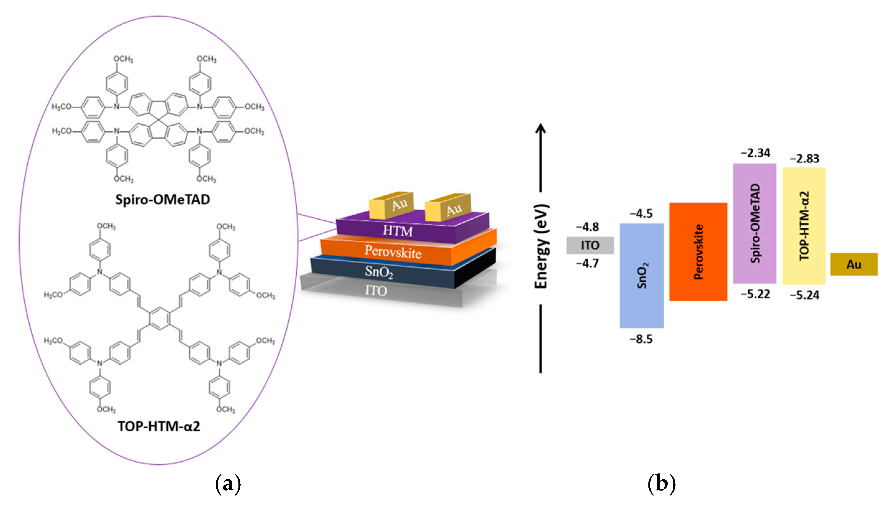
Figure 2.
Electrical properties of PSCs: (a) J-V characteristic of PSCs and (b) EQE.
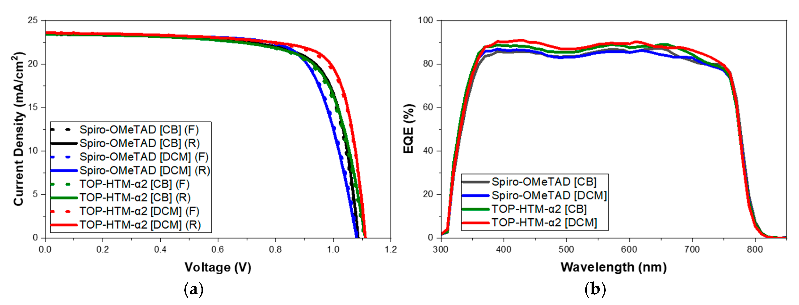
Figure 3.
AFM image of perovskite films: (a) without a hole transport layer, (b) after coating with Spiro-OMeTAD (CB), and (c) after coating with TOP-HTM-α2 (DCM).
Figure 3.
AFM image of perovskite films: (a) without a hole transport layer, (b) after coating with Spiro-OMeTAD (CB), and (c) after coating with TOP-HTM-α2 (DCM).

Figure 4.
Cross-sectional standard error of the mean images: (a) without a HTL, (b) after coating with Spiro-OMeTAD (CB), (c) after coating with Spiro-OMeTAD (DCM), (d) after coating with TOP-HTM-α2 (CB), and (e) after coating with TOP-HTM-α2 (DCM).
Figure 4.
Cross-sectional standard error of the mean images: (a) without a HTL, (b) after coating with Spiro-OMeTAD (CB), (c) after coating with Spiro-OMeTAD (DCM), (d) after coating with TOP-HTM-α2 (CB), and (e) after coating with TOP-HTM-α2 (DCM).
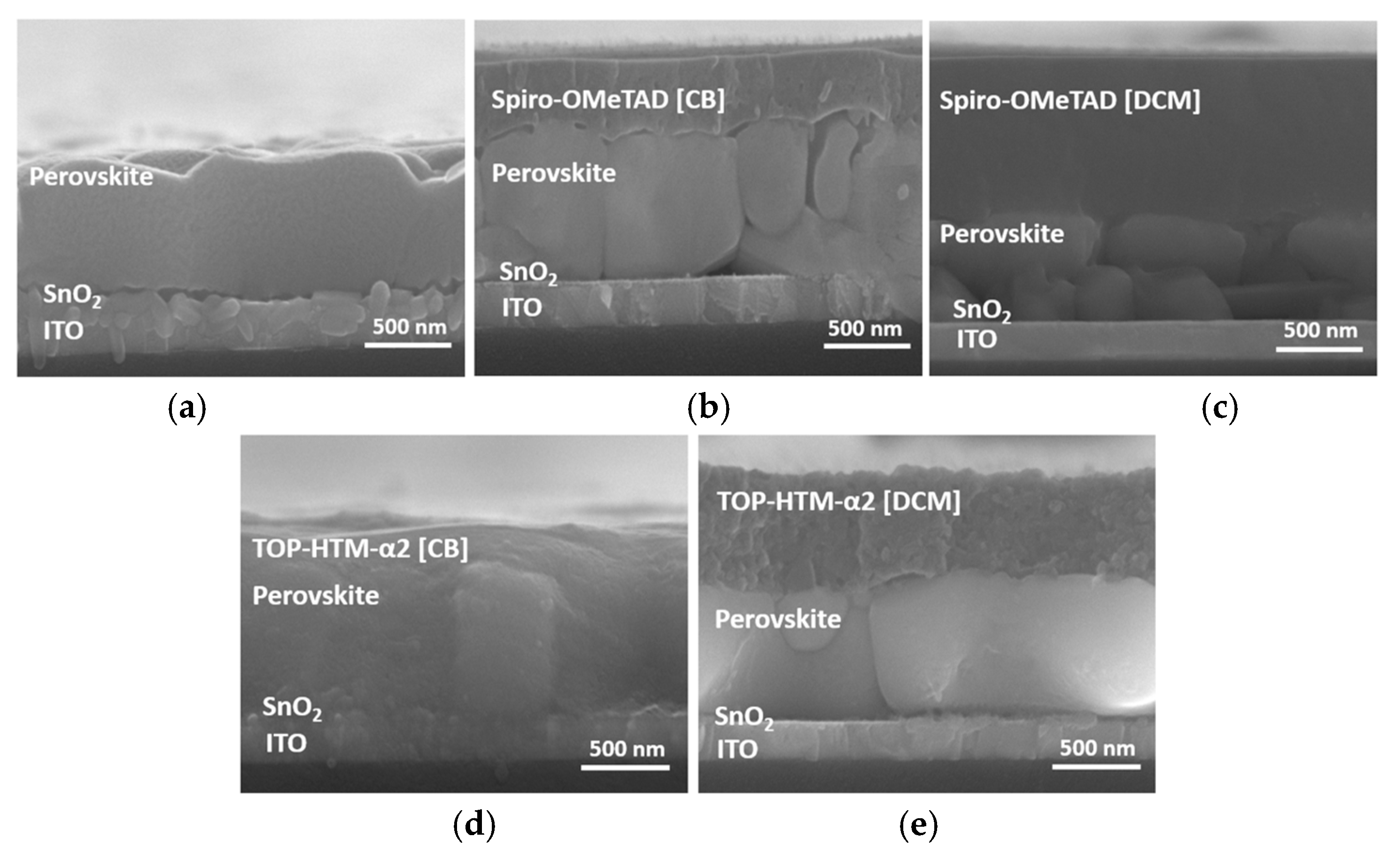
Figure 5.
XRD peaks of triple-cation perovskite films: (a) without a HTL, (b) after coating Spiro-OMeTAD (CB), (c) after coating with Spiro-OMeTAD (DCM), (d) after coating TOP-HTM-α2 (CB), and (e) after coating with TOP-HTM-α2 (DCM).
Figure 5.
XRD peaks of triple-cation perovskite films: (a) without a HTL, (b) after coating Spiro-OMeTAD (CB), (c) after coating with Spiro-OMeTAD (DCM), (d) after coating TOP-HTM-α2 (CB), and (e) after coating with TOP-HTM-α2 (DCM).
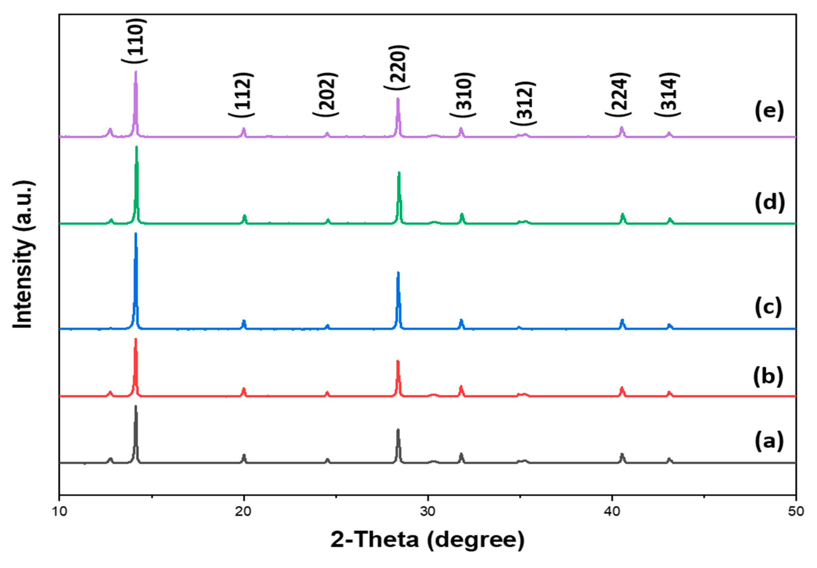
Figure 6.
Current–voltage curves of hole-only devices: (a) ITO/PEDOT:PSS/Perovskite/Spiro-OMeTAD (CB)/Au, (b) ITO/PEDOT:PSS/Perovskite/Spiro-OMeTAD (DCM)/Au, (c) ITO/PEDOT:PSS/Perovskite/TOP-HTM-α2 (CB)/Au, and (d) ITO/PEDOT:PSS/Perovskite/ TOP-HTM-α2 (DCM)/Au.
Figure 6.
Current–voltage curves of hole-only devices: (a) ITO/PEDOT:PSS/Perovskite/Spiro-OMeTAD (CB)/Au, (b) ITO/PEDOT:PSS/Perovskite/Spiro-OMeTAD (DCM)/Au, (c) ITO/PEDOT:PSS/Perovskite/TOP-HTM-α2 (CB)/Au, and (d) ITO/PEDOT:PSS/Perovskite/ TOP-HTM-α2 (DCM)/Au.

Table 1.
Summary of detailed performance parameters of PSCs.
| Sample | Jsc (mA/cm2) | Voc (V) | FF (%) | PCE (%) |
|---|---|---|---|---|
| Spiro-OMeTAD [CB] | 23.42 | 1.086 | 75.06 | 18.85 |
| Spiro-OMeTAD [DCM] | 23.54 | 1.081 | 72.88 | 18.55 |
| TOP-HTM-α2 [CB] | 23.42 | 1.110 | 71.77 | 18.67 |
| TOP-HTM-α2 [DCM] | 23.58 | 1.111 | 76.97 | 20.18 |
Disclaimer/Publisher’s Note: The statements, opinions and data contained in all publications are solely those of the individual author(s) and contributor(s) and not of MDPI and/or the editor(s). MDPI and/or the editor(s) disclaim responsibility for any injury to people or property resulting from any ideas, methods, instructions or products referred to in the content. |
© 2023 by the authors. Licensee MDPI, Basel, Switzerland. This article is an open access article distributed under the terms and conditions of the Creative Commons Attribution (CC BY) license (https://creativecommons.org/licenses/by/4.0/).
Share and Cite
MDPI and ACS Style
Lee, S.H.; Lim, S.B.; Kim, J.Y.; Lee, S.; Oh, S.Y.; Kim, G.M. An Alternative to Chlorobenzene as a Hole Transport Materials Solvent for High-Performance Perovskite Solar Cells. Crystals 2023, 13, 1667. https://doi.org/10.3390/cryst13121667
AMA Style
Lee SH, Lim SB, Kim JY, Lee S, Oh SY, Kim GM. An Alternative to Chlorobenzene as a Hole Transport Materials Solvent for High-Performance Perovskite Solar Cells. Crystals. 2023; 13(12):1667. https://doi.org/10.3390/cryst13121667
Chicago/Turabian StyleLee, Seung Ho, Seong Bin Lim, Jin Young Kim, Seri Lee, Se Young Oh, and Gyu Min Kim. 2023. "An Alternative to Chlorobenzene as a Hole Transport Materials Solvent for High-Performance Perovskite Solar Cells" Crystals 13, no. 12: 1667. https://doi.org/10.3390/cryst13121667
Note that from the first issue of 2016, this journal uses article numbers instead of page numbers. See further details here.