

Crystalline Nanodomains at Multifunctional Two-Dimensional Liquid–Metal Hybrid Interfaces


1
Department of Solid-Sate Sciences, Faculty of Science, Ghent University, Krijgslaan 281/S1, B-9000 Ghent, Belgium
2
Center for Environmental and Energy Research, Ghent University Global Campus, 119-5 Songdomunhwa-ro, Yeonsu-gu, Incheon 21985, Republic of Korea
*
Author to whom correspondence should be addressed.
Crystals 2023, 13(4), 604; https://doi.org/10.3390/cryst13040604
Submission received: 28 February 2023
/
Revised: 30 March 2023
/
Accepted: 31 March 2023
/
Published: 1 April 2023
(This article belongs to the Special Issue Synthesis and Characterization of Coordination Compounds)
Abstract
:Two-dimensional (2D) liquid–metal (LM) heterointerfaces with their tunable physicochemical characteristics are emerging platforms for the development of multifunctional hybrid nanostructures with numerous functional applications. From this perspective, the functionalization of LM galinstan nanoparticles (NPs) with crystalline nanodomains is a promising approach toward the synthesis of novel 2D hybrid LM heterointerfaces with unprecedented properties. However, the decoration of LM heterointerfaces with desired nanocrystalline structures is a challenging process due to simultaneous and intensive interactions between liquid–metal-based structures and metallic nanodomains. The present study discloses a facile and functional method for the growth of crystalline nanodomains at LM heterointerfaces. In this sonochemical-assisted synthesis method, acoustic waves provide the driving force for the growth of ultra-fine crystalline nanodomains on the surface of galinstan NPs. The galinstan NPs were initially engulfed within carbon nanotube (CNT) frameworks, to prevent intensive reactions with surrounding environment. These CNT frameworks furthermore separate galinstan NPs from the other products of sonochemistry reactions. The following material characterization studies demonstrated the nucleation and growth of various types of polycrystalline structures, including Ag, Se, and Nb nanodomains on 2D heterointerfaces of galinstan NPs. The functionalized galinstan NPs showed tunable electronic and photonic characteristics originated from their 2D hybrid interfaces.
1. Introduction
Galinstan-based structures have recently emerged as a novel family of advanced materials with interesting physicochemical characteristics, including room-temperature fluidity, high conductivity, facile synthesis, and low toxicity [1,2,3,4]. Galinstan is the room-temperature liquid alloy of Ga-In-Sn. The semiconducting property of naturally developed atomically thin gallium oxide layers on the surface of galinstan NPs is one the main characteristics of these hybrid nanostructures [5,6,7]. The heterointerfaces between LM galinstan and their surrounding environment witness various types of chemical interactions and charge transfer phenomena which are beneficial for a wide range of functional applications from biosensing [8] and biomimicry systems [9] to photonic [10] and catalysis [11].
The high surface tension of LM galinstan effectively suppresses the fragmentation of this room-temperature LM alloy into ultra-fine nanoparticles. The ultrasonic waves provide strong mechanical forces for functional applications [12]. The outward explosion and the inward implosion of bubbles during the sonication process produce microjets and shock waves at ultrasound speeds. These mechanical forces accelerate moving particles inside of reaction liquid medium with the speed of several hundred meters per second (m/s) [13]. The following collisions of high energy/high speed microjets provide strong shear forces for drastic mechanical fragmentation of materials, known as the sono-fragmentation process [14,15,16]. Consequently, the acoustic activated energy can effectively supply the driving force for the synthesis of galinstan NPs through fragmentation [17]. Furthermore, the hot-spot regions in ultrasonic generated bubbles experience high level of temperature (5000 k) and pressure (1000 atm) during the cavitation process [18,19]. The magnitude of generated energy in hot-spot regions of ultrasonic bubbles reaches the value of 13 eV [20]. The hot-spot regions may also experience high-energy particle collision, plasma formation [20,21], and even nuclear fusion [22]. Such an extraordinary condition in hot-spots can induce unusual physical and chemical states and, therefore, can provide the feasible conditions for initiation and continuation of chemical reactions, followed by the growth of nanostructured materials [23,24,25]. In sonochemical synthesis, high-pressure bubbles contain ionic species and chemical radicals. These species originate from the chemical solutions and precursors in the reaction environment [26]. In the sonochemical treatment of homogenous solutions, both chemical and physical factors work constructively toward the synthesis of nanostructured materials [27]. During the sonochemical synthesis of heterogeneous mixtures, the physical effects are dominant factors during the synthesis process [28]. There are two main sonochemistry synthesis mechanisms. In the primary version of sonochemistry, the reactive species and precursors participate in the creation of hot-spot regions (Figure 1a). The diffusion of microscale compounds into the bubble core provides conditions for precursors to experience the main effects of cavitation phenomenon. Consequently, it orchestrates the required conditions for the successful interactions between the ionic species and precursors inside of bubbles [29]. Unusual structures are synthesized by primary sonochemistry due to extremely unusual conditions in the core of hot-spot regions [30]. In detail, upon the eruption of magma matter into the surrounding environment, the extremely hot materials suddenly quench at the extraordinary cooling rate of 1010 K/s [31]. The cooling rate is intensified due to the extensive distribution of cavitation bubbles into the reaction medium [31]. These combined conditions facilitate the growth of nanostructures in different shapes and compositions. The secondary sonochemistry is the other mechanism where the chemical reactions occur outside of bubbles in the liquid phase (Figure 1a) [30]. During this process, the scattered radicals and ions interact with the reaction medium. In the secondary sonochemistry, the synthesis conditions are free from the extraordinary physical conditions of hot-spots; therefore, the synthesized materials possess properties similar to the conventional nanostructures [12,29]. In sonochemical-assisted synthesis, the composition and concentration of precursors have tremendous impact on the morphology of synthesized nanostructures [32,33]. A typical example is the sonochemical-assisted growth of nano-sized ZnO [33,34]. It was observed that the increase of precursor concentration altered the ZnO morphology from 1D nanorods to 2D nanosheets and nanoflakes, while the higher concentration of precursors favors the multidirectional growth of nanostructures [33,34]. Therefore, the control of precursor concentration fundamentally affects the sonochemical reactions and prompts the synthesis of new materials with stabilized growth directions [35].
Recently, the sonochemical-assisted technique was employed to develop various types of LM-based composite particles for functional applications [36,37,38]. A recent study reported the synthesis of nano/micro-sized Ga/Ni co-catalysts for biofuel conversion to value-added byproducts. In this technique, catalyst materials (Ni and NiO2) were employed in the sonication process to decorate the surface of gallium-based particles via the ultrasonic approach [36]. In another research study, manganese oxide [37] and molybdenum oxysulfide [38] shells were developed on the gallium-based NPs via a sonochemical synthesis approach. In these methods, the highly active surface of gallium-based NPs interacts directly with the chemical agents in the presence of strong ultrasonic waves, resulting in the synthesis of unregularly deformed NPs and nanostructures. Furthermore, due to the formation of 2D composite oxide structures on the surface of active gallium-based NPs, these nanostructures lose the high-conductive characteristics of their surface. The sonochemical-assisted synthesis of galinstan NPs in metal–ionic solutions enabled the growth of crystalline nanostructures on the surface of liquid metal NPs [17]. Here, the galinstan NPs act as the nucleation sites for growth of various nanostructures, including metallic nanodomains and nanodisks. The acoustic-assisted decoration of galinstan NPs with crystalline nanodomains enables the development of 2D liquid–metal hybrid interfaces. However, there are two main challenges that originated from the uncontrolled synthesis conditions during sonochemistry technique. These two challenges are the unwanted progressive alloying of galinstan with other precursors [39] and the growth of undesired nanostructures at heterointerfaces. In the present research, a novel approach is introduced for the controlled sonochemical synthesis of crystalline nanodomains on the surface of galinstan NPs. The new concept of development of CNT-engulfed functionalized gallium-based NPs is developed here by using the principles of sonochemistry (Figure 1b). The CNT frameworks suppress the intense interaction between the surface of galinstan NPs and precursors in sonochemical synthesis environment. Consequently, the facile and controlled nucleation and growth of ultra-fine crystalline nanodomains on two-dimensional LM hybrid interfaces of galinstan NPs is achieved without considerable damage to the galinstan NPs. The sonochemical synthesis enables the growth of crystalline Se, Ag, and Nb nanodomains on the surface of galinstan NPs. This work introduces a functional, feasible, and low-cost synthesis approach that offers a great opportunity for the development of functionalized liquid metal NPs with adjustable surface characteristics and tunable electronic properties for numerous functional applications.
2. Materials and Methods
To synthesize liquid metal NPs, 20 mg of galinstan alloy (Indium Corporation, Upstate New York. USA) was initially immerged into a glass vial filled with ethyl alcohol anhydrous (Merck). The glass vial contained 0.1 M HCl. The slurry was probe-sonicated for an hour (20 Hz, 380 W) while the temperature of slurry was kept at 20 °C. Then, the solution was kept for 8 h to reach the uniform distribution of ultra-fine NPs. The slurry of ultrafine nanoparticles was then extracted from the upper part of container for further synthesis process. Our observation showed that the size of NPs was in the range of 50 nm to 20 nm. To synthesize CNT frameworks, 1.0 wt.% CNT was later incorporated into galinstan NPs and sonicated for an hour. To grow Ag, Se, and Nb nanodomains on the surface of galinstan NPs, different solutions were prepared by sonication of AgCl4, SeCl4, and NbCl5 in ethyl alcohol anhydrous. The slurry of CNT-engulfed galinstan framework (CNT@ galinstan) was probe-sonicated in the ionic solutions with different concentrations (0.1, 0.2, and 0.5 μmol/L) for an hour (20 Hz, 380 W). After sequential centrifugation and ultrasonication process of the composite frameworks, the functionalized NPs were extracted and separated from CNT clusters and other byproducts for further characterization process (Figure 1d,e).
For material characterization, the functionalized NPs were extracted, dried in controlled atmosphere, and then investigated by various methods. The micro-Raman spectrometer (micro-Raman HORIBA Lab Ram ARAMIS) equipped with λ = 530 nm laser was employed for characterization of NPs. The λ = 320 nm laser was used during Raman studies to extract the PL spectra of synthesized nanostructures. The X-ray photoelectron spectroscopy (XPS) was later employed for analysis of surface composition of galinstan NPs after functionalization (XPS-Scientific Theta Probe). The field-emission scanning electron microscope (FESEM, JEOL 7800F), and transmission electron microscope (TEM, JEOL-JEM-F200) were coupled with their energy dispersive spectrometers (EDS) and selected-area electron diffraction (SAED) equipment to investigate the structural characteristics of synthesized nanostructures. For SEM studies, the extracted nanostructures (in ethyl alcohol anhydrous) were drop-casted on the Au coated silicon substrates and were dried in controlled atmosphere at room temperature. For TEM studies, the extracted suspensions of NPs from centrifugation/sonication process were drop-casted on TEM sample holders (formvar/carbon-supported copper grids/400 mesh) and were dried and kept inside of the atmosphere-controlled desiccator before TEM studies.
3. Results and Discussion
3.1. Synthesis Method
To functionalize the 2D heterointerface of galinstan NPs with crystalline nanodomains, it was necessary to grow ultrafine nanostructures on the outer shell of galinstan NPs. However, the conventional synthesis of galinstan NPs in metal–ionic solutions has several main drawbacks. The main drawback of the sonochemical-assisted synthesis is the intense reaction of galinstan NPs with ionic metals and other nanostructures. In detail, the NPs act as the nucleation sites of synthesized nanostructures. Regarding the sonochemical reactivity and intensity of interactions between LM galinstan and nucleated structures, different types of synthesized nanostructures were grown and formed during the sonochemical synthesis of functionalized galinstan NPs in metal ionic solutions. The famous example of this process is the growth of Ga-Al alloying nanostructures on the surface of galinstan NPs [39,40]. It was shown that GaxAly needle-like nanostructures were grown on the surface of galinstan NPs through galvanic replacement mechanism [39,40]. At high-level Ag concentration, the Ga-Ag nanostructures were developed due to intense galvanic replacement and alloying process according to the following reaction [17]:
Ga0 + 3Ag+ → Ga3+ + 3Ag0
In the present study, in the lack of CNT frameworks, we also observed the growth of different undesired nanostructures during the sonochemical synthesis of galinstan NPs in metal–ionic solutions (Figure 2). For example, the growth of Se-rich and Ga-Se-rich nanostructures were extensively observed due to sonochemical reactions between galinstan NPs and Se-containing solution. At high Se concentration, the Ga-Se nanosheets grew extensively with various compositions. Figure 2a shows SEM image of a typical Ga-Se rich nanosheet with its corresponding EDS map analysis. Furthermore, galinstan NPs acted as the nucleation sites for other types of Se-rich structures (marked in Figure 2b). Figure 2b and its corresponding EDS maps depict the simultaneous growth of Se nanorods and nanoparticles on the surface of galinstan NPs. Figure 2c depicts agglomerated Se NPs and their corresponding EDS analysis. The agglomerated Se NPs were observed in the products of sonochemical synthesis process of the samples containing high concentration of ionic Se (0.5 μmol/L). The reason that we used various concentrations of ionic solutions (Ag, Se, and Nb) was to evaluate the effects of sonochemical synthesis conditions on the growth of crystalline nanodomains on the surface of galinstan NPs. Table 1 provides the specifications of various types of Se-rich nanostructures and their corresponding sonochemical synthesis conditions. These structures are undesired products of sonication process since they grow at the expense of consumption of valuable galinstan NPs during sonochemical reactions. To tackle this challenge, we developed a synthesis approach, where galinstan NPs were engulfed in CNT networks (Figure 1c). In this approach, the incorporation of CNT framework into liquid–metal NPs represents a fundamentally novel assembly of advanced 2D hybrid interfaces with principally new properties. Furthermore, CNTs engulf larger by-products of sonication process that inevitably formed during the sonochemical synthesis reactions. These unwanted nanostructures can be separated from synthesis environment via sequential sonication due to the weight differences (Figure 1d). CNT is a highly active porous structure that can extensively interact with metal–ionic agents during the sonication process. Therefore, it can actively suppress the intense invasion of ionic agents to the surface of galinstan NPs during long-term sonochemical synthesis. Ionic species can still diffuse through the CNT porous network and reach to the surface of galinstan NPs to enable the growth and nucleation of low-dimensional crystalline nanodomains at 2D heterointerfaces. It further diminishes the serious damages into liquid metal NPs due to intense progressive sonochemical reactions. The extracted galinstan NPs (Figure 1e) were later investigated by various material characterization techniques. The shielding role of CNT aside, the highly conductive carbon-based framework around galinstan NPs enabled the facile and rapid charge transfer process from heterointerface of liquid metal NPs to the surrounding environment [41,42,43]. Furthermore, due to the sp2 hybridized structure, CNT frameworks are excellent electron acceptor nanostructures with the capacity of high-spatial separation of electron–hole pairs [44]. Moreover, the introduction of doping elements into porous network of CNT can considerably increase the charge transport and ionic penetration through the CNT framework. As an example, the decoration of CNT framework with Se nanoparticles resulted in an 11-fold improvement of current density in CNT/Se framework for CO2 catalysis [45]. In other cases, decoration of CNT with niobium nanostructures considerably improved the limits of dopamine detection to nano-molar levels due to the increased ion transfer rate [46].
3.2. Materials Chracterization
The extracted galinstan NPs were studied by various characterization methods. The Raman and photoluminescence analysis accompanied by TEM and X-ray photoelectron spectroscopy were employed to characterize the synthesized nanostructures. Figure 3a shows a single galinstan NP after growth of Ag nanodomains on its surface. The sequential centrifugation/sonication process enabled the separation of functionalized NPs from their CNT network for characterization. The TEM image from the surface of galinstan NP depicts the growth of ultrafine poly-crystalline Ag nanodomains. The corresponding TEM image from the Ag nanodomains shows the growth of (111) plane of Ag with interlayer spacing of 0.4 nm (Figure 3a) [39]. The crystalline planes were found highly ordered in crystalline nanodomain. The following SAED patterns were collected from the surface of Ag-functionalized galinstan NPs. The SAED patterns in Figure 3a show the fringes of (111), (200), and (220) crystalline planes highly matched to the ICSD 98-018-0878 belonging to the crystalline plane of Ag [39]. By changing the location of SAED spectrometer, we even identified different Ag crystalline planes, confirming the polycrystalline nature of synthesized Ag nanodomains on the surface of galinstan NPs. We further investigated the Raman spectra of galinstan-Ag heterointerfaces (Figure 3b). In Figure 3b, the Raman peaks of A1g, A2g, and A3g are the characteristics of Ga-O bonds related to the ultra-thin surface oxide films of galinstan NPs [47,48]. The characteristic Raman peak of Ag is not characterized since the Ag is not Raman-active material [17]. Therefore, the following PL spectroscopy tests were conducted to show the evidence of presence of Ag nanodomains on galinstan NPs and their effects on their photonic properties. The inset in the graph of Figure 3b depicts the PL spectra of galinstan-Ag NPs. The single shallow shoulder at λ= 360 nm is attributed to the 2D surface oxide films of galinstan (Ga2O3) [49]. The other strong peak at the vicinity of λ = 410~430 is assigned to the resonance absorption wavelength of Ag nanodomains [50]. The evidence of surface plasmon resonance (SPR) phenomenon was also observed by the detection of two broad peaks at λ = 550 nm and λ = 700 nm related to the plasmonic characteristics of Ag nanodomains [50]. The photonic local field enhancement and SPR occur at heterointerfaces between Ag nanodomains at 2D Ga2O3. Consequently, the SPR characteristic peaks appear at PL spectra of galinstan-Ag heterointerfaces. This observation is highly valuable since it confirms the occurrence of plasmonic phenomenon at the heterointerfaces between ultra-thin 2D semiconductor films (Ga2O3 on galinstan NPs) and plasmonic Ag nanodomains. Therefore, this heterointerface could support the generation of SPR phenomenon. This is a functional property for a wide range of applications, including photocatalysis, energy generation, and biosensing targets [51].
The following experiments on the galinstan-Se nanostructures showed the growth of polycrystalline Se nanodomains on the heterointerfaces. Figure 3c depicts the fully covered surface of galinstan NPs with Se nanodomains. Technically, Se is highly reactive material that can intensively interact with galinstan LM particles. Therefore, the controlled growth of Se nanodomains on the galinstan NPs was found to be quite a challenging process compared with the growth of Ag and Nb nanostructures on the galinstan NPs. The TEM image shows the high-crystalline nature of Se nanodomains on the surface of galinstan NPs (Figure 3c). The interlayer distance of d = 0.37 nm is attributed to the (100) crystalline plane of Se, which is highly matched to the ICSD 22251 belonging to the crystalline structure of Se [52,53]. The following SAED patterns from the heterointerfaces show characteristic rings of (100) and (120) crystalline planes of Se (Figure 3c) [52,53]. Similar to previous observations on the growth of Ag nanodomains, these results also confirm the polycrystalline nature of Se nanodomains synthesized during the sonochemical reactions. It further reinforces this idea that the nucleation and growth of nanodomains occur individually at different locations on the galinstan NPs, and then the process continues until nanodomains fully cover the surface of galinstan NPs. The micro-Raman spectra of galinstan-Se nanostructures show the E1 and A1 vibrational modes of trigonal Se at 142 cm−1 and 233.8 cm−1, respectively (Figure 3d) [17]. The two individual shallow peaks at 248 cm−1 and 253 cm−1 belong to the Ga-Se structure [17]. The A1g peak at 132 cm−1 is also attributed to the Ga-Se alloying compounds [17]. The PL study on the same sample demonstrated two broad peaks at the 340 nm and 558 nm. These peaks are related to, respectively, the excitation and emission peaks of Se nanostructures [54]. The excitation of surface plasmon is one of the main characteristics of Se nanostructure. The red tint of synthesized galinstan-Se NPs has been ascribed to the corresponding excitation of the surface plasmon resonance of the synthesized monolithic Se structures [54]. It appears that the heterointerfaces between galinstan NPs and Se crystalline nanodomains possess a high level of plasmonic feature. The Se nanostructures are well known for their photonic, photovoltaic, semiconducting, antimicrobial, anti-infection, and antioxidant properties; therefore, these nanostructures can extensively contribute the functionalities of galinstan NPs for a wide range of applications [55].
The following characterization tests showed that Nb nanodomains were developed on the surface of galinstan NPs by the sonochemistry method. The TEM studies confirmed the polycrystalline nature of Nb nanodomains (Figure 3e). The Nb nanodomains with small dimensions (~5 nm) grew extensively on the galinstan NPs. The typical TEM image and corresponding SAED patterns depict the growth of (101) and (220) planes attributed to the crystalline plane of Nb (ICSD 55957) (Figure 3e) [56]. The Raman spectroscopy consequently showed characteristic peaks of Nb-O bonding at 160 cm−1, 400 cm−1, 632 cm−1, and 792 cm−1 (Figure 3f) [57]. The PL intensity of galinstan-Nb structures demonstrated three individual broad peaks in the vicinity of 410 nm (3.02 eV), 460 nm (2.69 eV), and 500 nm (2.47 eV) wavelengths (Figure 3f). These peaks are assigned to the PL peaks of the Nb-O bonds [58]. Niobium and niobium-based compounds are of high interest for superconducting applications. However, niobium also shows an insulating niobium oxide layer with distinguished dielectric properties. The detection of Nb-O bonds can be attributed to the immediate oxidation of Nb nanostructures in ambient atmosphere [58]. Since the characterization tests were conducted under ambient condition, the immediate passivation of Nb nanoparticles is expected during the investigations. Generally, the TEM observations accompanied by Raman and PL spectroscopy techniques confirmed the polycrystalline nature of developed nanodomains on the galinstan NPs. Interestingly, the photonic properties of functionalized NPs were extensively different from each other. The plasmonic Ag and Se nanodomains were coupled with the 2D surface oxide semiconductor film of galinstan NPs (Ga2O3), resulting in the detection of resonance absorption, SPR, and excitation maximum phenomena during the PL spectroscopy measurements. Therefore, the 2D heterointerfaces of galinstan NPs possess visible-light plasmonic characteristics, providing a unique opportunity for photonic applications.
The investigations on the XPS spectra of synthesized nanostructures provide extensive information on the composition, oxidation states, and valence band maximum (VBM) at 2D heterointerfaces of nanostructures. Figure 4 shows the results of XPS and monochromatic XPS measurements of the galinstan NPs with Ag, Se, and Nb nanodomains. Figure 4a shows two individual and sharp peaks of Ag 3d3/2 and Ag 3d5/2 at 373 eV and 367 eV, confirming the growth of Ag nanodomains at heterointerfaces. The following investigation on Ga 3d XPS peaks shows that the intensity of these peaks considerably decreased (Figure 4b) and slightly shifted to lower binding energies after functionalization of galinstan with Ag nanodomains. It confirms the alteration of binding energies at galinstan-Ag heterointerfaces. The O 1s peak also shifted to lower binding energies after the growth of Ag nanodomains on galinstan NPs (Figure 4c). It further confirms the alteration of oxidation states at heterointerfaces. The lower binding energies of O 1s peak is attributed to their lower oxidation states or chemical shift due to developed chemical bonds. The following experiments on the galinstan-Se nanostructures showed two Se 3d3/2 and 3d5/2 peaks at 58.8 eV and 54.7 eV, respectively (Figure 4d). The peak at 58.8 eV shows the presence of Se4+ species, such as selenate compounds, in nanostructures [58]. The functionalization of galinstan with Se nanodomains also affected the Ga 3d peak. The Ga 3d peak shifted to lower binding energy, confirming the alteration of binding energies of Ga atoms at the heterointerfaces after functionalization with Se nanodomains (Figure 4e). Considering higher electronegativity of Se (2.15 eV) than that of Ga (1.81 eV), the electron density around Se atoms is expected to be higher than that around Ga atoms. Therefore, the binding energies decreased and shifted negatively. More importantly, the intensity of Ga 3d peak decreased considerably after functionalization with Se nanodomains. The O 1s spectra of galinstan-Se heterointerfaces also shifted to higher binding energies, compared with those of galinstan NPs. The higher binding energies of O 1s spectra is an indication of developed chemical interactions between Ga and Se atoms. It represents the changes in the oxidation states of Ga atoms. Moreover, the study on the galinstan-Nb heterointerfaces showed two sharp and individual Nb 3d peaks at 207.4 eV and 210. 3 eV (Figure 4g). It further conforms the growth of Nb on the surface of galinstan NPs. After functionalization by Nb nanodomains, the intensity of Ga 3d peak decreased considerably and shifted to higher binding energies (Figure 4h). The O 1s peak of the galinstan-Nb interface did not considerably shift. Furthermore, the intensity of the O 1s peak increased slightly, confirming the higher level of oxidation at galinstan-Nb interfaces. The XPS studies provided the evidence of development of various types of heterointerfaces between galinstan NPs and metallic (Ag, Se, and Nb) nanodomains. The alteration of O 1s XPS spectra in galinstan-Ag and galinstan-Se nanodomains confirms the development of structural bonding between galinstan atoms and Ag and Se nanodomains. Therefore, it is expected that some level of electron exchange and alloying occurred at the heterointerfaces.
We further investigated the VBM of developed heterointerfaces by monochromatic XPS equipment (Figure 4j). The VBM of galinstan NPs decreased after their functionalization with the Ag, Nb, and Se nanodomains. The VBM of galinstan NPs decreased from 2.8 eV to 2.4 eV after growth of Ag nanodomains on the heterointerfaces (Figure 4j). Consequently, the VBM values decreased to 1.99 eV after growth of Nb nanodomains and later decreased to the value of 1.54 eV after growth of Se nanodomains on galinstan heterointerfaces (Figure 4j). The alteration of VBM of galinstan NPs after growth of crystalline nanodomains confirms the tunability of electronic properties of developed two-dimensional liquid–metal hybrid interfaces. The PL measurements also showed the multiple-peak configurations in photoluminescence spectra of samples (Figure 3b,d,f) confirming that their complex energy states and electronic band alignments originated from their mixed structure and developed hybrid 2D heterointerfaces. Furthermore, it depicts how the interaction between the 2D surface oxide semiconductor films of galinstan NPs with crystalline nanodomains can considerably alter the electronic properties of developed nanostructures. The tunable electronic properties accompanied by distinguished photonic characteristics of developed heterointerfaces provide unique opportunities for a wide range of beneficial applications in photonic and solar-power-based technologies.
4. Conclusions
The current study has introduced a facile functionalization approach for development of multifunctional 2D liquid–metal hybrid heterointerfaces through the growth of crystalline metallic nanodomains on the surface of galinstan NPs engulfed in CNT frameworks. The sonochemical synthesis enabled the controlled growth of Ag, Se, and Nb nanodomains on the surface of galinstan NPs. The engulfment of galinstan NPs in CNT network provided a controllable condition during the synthesis process to suppress the intense interactions between ionic metal species and liquid galinstan. The materials characterization confirmed the growth of polycrystalline metallic nanodomains on the surface of galinstan NPs. The polycrystalline Ag, Se, and Nb nanodomains partially or fully covered the surface of galinstan NPs. This created unique heterointerfaces between galinstan NPs and crystalline nanodomains with distinguished electronic characteristics. For example, the coupling of 2D surface oxide film of galinstan with Ag and Se nanodomains was accompanied by the occurrence of surface plasmon resonance effects and observation of excitation and emission photoluminescence phenomena. The alteration of energy states and valance band maximum values after development of 2D hybrid heterointerfaces was observed as the results of growth of nanodomains on 2D liquid metal heterointerfaces. The tunable electronic characteristics of theses hybrid interfaces are highly promising for a various functional applications.
Author Contributions
Introduction of concept, experiments, and original draft preparation, M.K.A. and N.S.L.; Supervision, S.Z. All authors have read and agreed to the published version of the manuscript.
Funding
This research was funded by Ghent University Global Campus (Republic of Korea).
Data Availability Statement
Available upon the request from the authors.
Acknowledgments
This work was supported by research program of the Ghent University Global Campus.
Conflicts of Interest
The authors declare no conflict of interest.
References
- Kalantar-Zadeh, K.; Tang, J.; Daeneke, T.; O’Mullane, A.P.; Stewart, L.A.; Liu, J.; Majidi, C.; Ruoff, R.S.; Weiss, P.S.; Dickey, M.D. Emergence of liquid metals in nanotechnology. ACS Nano 2019, 13, 7388–7395. [Google Scholar] [CrossRef] [PubMed]
- Chiew, C.; Morris, M.J.; Malakooti, M.H. Functional liquid metal nanoparticles: Synthesis and applications. Mater. Adv. 2021, 2, 7799–7819. [Google Scholar] [CrossRef]
- Chiechi, R.C.; Weiss, E.A.; Dickey, M.D.; Whitesides, G.M. Eutectic gallium-indium (EGaIn): A moldable liquid metal for electrical characterization of self-assembled monolayers. Angew. Chem. Int. Ed. 2008, 47, 142–144. [Google Scholar] [CrossRef]
- Lin, Y.; Liu, Y.; Genzer, J.; Dickey, M.D. Shape-transformable liquid metal nanoparticles in aqueous solution. Chem. Sci. 2017, 8, 3832–3837. [Google Scholar] [CrossRef] [PubMed] [Green Version]
- Karbalaei Akbari, M.; Zhuiykov, S. Dynamic self-rectifying liquid metal–semiconductor heterointerfaces: A platform for development of bioinspired afferent system. ACS Appl. Mater. Interfaces 2021, 13, 60636–60647. [Google Scholar] [CrossRef]
- Karbalaei Akbari, M.; Verpoort, F.; Zhuiykov, S. Plasma-enhanced elemental enrichment of liquid metal interfaces: Towards realization of GaS nanodomains in two-dimensional Ga2O3. Appl. Mater Today 2022, 27, 101461. [Google Scholar] [CrossRef]
- Karbalaei Akbari, M.; Zhuiykov, S. Plasma-assisted growth of two-dimensional Ga2O3/Gas heterophases on liquid alloy substrate for nanoelectronic applications. Mater. Sci. Forum 2022, 1075, 49–55. [Google Scholar] [CrossRef]
- Li, H.; Qiao, R.; Davis, T.P.; Tang, S.-Y. Biomedical applications of liquid metal nanoparticles: A critical review. Biosensors 2020, 10, 196. [Google Scholar] [CrossRef]
- Karbalaei Akbari, M.; Zhuiykov, S. A bioinspired optoelectronically engineered artificial neurorobotics device with sensorimotor functionalities. Nat. Commun. 2019, 10, 3873. [Google Scholar] [CrossRef] [Green Version]
- Karbalaei Akbari, M.; Verpoort, F.; Zhuiykov, S. State-of-the-art surface oxide semiconductors of liquid metals: An emerging platform for development of multifunctional two-dimensional materials. J. Mater. Chem. A 2021, 9, 34–73. [Google Scholar] [CrossRef]
- Sun, X.; Li, H.Y. Recent progress of Ga-based liquid metals in catalysis. RSC Adv. 2022, 12, 24946–24957. [Google Scholar] [CrossRef] [PubMed]
- Pokhrel, N.; Vabbina, P.K.; Pala, N. Sonochemistry: Science and engineering. Ultrason. Sonochem. 2016, 29, 104–128. [Google Scholar] [CrossRef] [PubMed]
- Doktycz, S.; Suslick, K. Interparticle collisions driven by ultrasound. Science 1990, 247, 1067–1069. [Google Scholar] [CrossRef] [Green Version]
- Gopi, K.R.; Nagarajan, R. Advances in nanoalumina ceramic particle fabrication using sonofragmentation. IEEE Trans. Nanotechnol. 2008, 7, 532–537. [Google Scholar] [CrossRef]
- Pérez-Maqueda, L.A.; Duran, A.; Pérez-Rodríguez, J.L. Preparation of submicron talc particles by sonication. Appl. Clay Sci. 2005, 28, 245–255. [Google Scholar] [CrossRef]
- Zeiger, B.W.; Suslick, K.S. Sonofragmentation of molecular crystals. J. Am. Chem. Soc. 2011, 137, 14530–14533. [Google Scholar] [CrossRef]
- Karbalaei Akbari, M.; Hai, Z.; Wei, Z.; Ramachandran, R.K.; Detavernier, C.; Patel, M. Sonochemical functionalization of the low-dimensional surface oxide of galinstan for heterostructured optoelectronic applications. J. Mater. Chem. C 2019, 7, 5584–5595. [Google Scholar] [CrossRef]
- Bang, J.H.; Suslick, K.S. Applications of ultrasound to the synthesis of nanostructured materials. Adv. Mater. 2010, 22, 1039–1059. [Google Scholar] [CrossRef]
- Xu, H.; Zeiger, B.W.; Suslick, K.S. Sonochemical synthesis of nanomaterials. Chem. Soc. Rev. 2013, 42, 2555–2567. [Google Scholar] [CrossRef] [PubMed] [Green Version]
- Flannigan, D.J.; Suslick, K.S. Plasma formation and temperature measurement during single-bubble cavitation. Nature 2005, 434, 52–55. [Google Scholar] [CrossRef] [PubMed] [Green Version]
- Didenko, Y.T.; McNamara, W.B.; Suslick, K.S. Molecular emission from single-bubble sonoluminescence. Nature 2000, 407, 877–879. [Google Scholar] [CrossRef] [PubMed]
- Taleyarkhan, R.P.; West, C.D.; Cho, J.S.; Lahey, R.T.; Nigmatulin, R.I.; Block, R.C. Evidence for nuclear emissions during acoustic cavitation. Science 2002, 295, 1868–1873. [Google Scholar] [CrossRef] [Green Version]
- Suslick, K.S.; Hyeon, T.; Fang, M. Nanostructured materials generated by high-intensity ultrasound: Sonochemical synthesis and catalytic studies. Chem. Mater. 1996, 8, 2172–2179. [Google Scholar] [CrossRef]
- Mdleleni, M.M.; Hyeon, T.; Suslick, K.S. Sonochemical synthesis of nanostructured molybdenum sulfide. J. Am. Chem. Soc. 1998, 120, 6189–6190. [Google Scholar] [CrossRef]
- Calderón-Jiménez, B.; Montoro Bustos, A.R.; Pereira Reyes, R. Novel pathway for the sonochemical synthesis of silver nanoparticles with near-spherical shape and high stability in aqueous media. Sci. Rep. 2022, 12, 882. [Google Scholar] [CrossRef] [PubMed]
- Henglein, A.; Herburger, D.; Gutierrez, M. Sonochemistry: Some factors that determine the ability of a liquid to cavitate in an ultrasonic field. J. Phys. Chem. 1992, 96, 1126–1130. [Google Scholar] [CrossRef]
- Suslick, K.S.; Choe, S.-B.; Cichowlas, A.A.; Grinstaff, M.W. Sonochemical synthesis of amorphous iron. Nature 1991, 353, 414–416. [Google Scholar] [CrossRef]
- Zhang, L.; Belova, V.; Wang, H.; Dong, W.; Möhwald, H. Controlled cavitation at nano/microparticle surfaces. Chem. Mater. 2014, 26, 2244–2248. [Google Scholar] [CrossRef]
- Thompson, L.H.; Doraiswamy, L.K. Sonochemistry: Science and engineering. Ind. Eng. Chem. Res. 1999, 38, 1215–1249. [Google Scholar] [CrossRef]
- Martínez, R.F.; Cravotto, G.; Cintas, P. Organic Sonochemistry: A Chemist’s timely perspective on mechanisms and reactivity. J. Org. Chem. 2021, 86, 13833–13856. [Google Scholar] [CrossRef]
- Kis-Csitári, J.; Kónya, Z.; Kiricsi, I. Sonochemical Synthesis of Inorganic Nanoparticles. In Functionalized Nanoscale Materials, Devices and Systems. NATO Science for Peace and Security Series B: Physics and Biophysics; Vaseashta, A., Mihailescu, I.N., Eds.; Springer: Dordrecht, The Netherlands, 2008. [Google Scholar]
- Tuziuti, T.; Yasui, K.; Kato, K. Influence of degree of gas saturation on multibubble sonoluminescence intensity. J. Phys. Chem. A 2011, 115, 5089–5093. [Google Scholar] [CrossRef]
- Jung, S.-H.; Oh, E.; Lee, K.-H.; Yang, Y.; Park, C.G.; Park, W.; Jeong, S.-H. Sonochemical preparation of shape-selective ZnO nanostructures. Cryst. Growth Des. 2008, 8, 265–269. [Google Scholar] [CrossRef]
- Vabbina, P.K.; Karabiyik, M.; Al-Amin, C.; Pala, N.; Das, S.; Choi, W.; Saxena, T.; Shur, M. Controlled synthesis of single-crystalline ZnO nanoflakes on arbitrary substrates at ambient conditions. Part. Part. Syst. Charact. 2014, 31, 190–194. [Google Scholar] [CrossRef]
- Nemamcha, A.; Rehspringer, J.-L.; Khatmi, D. Synthesis of palladium nanoparticles by sonochemical reduction of palladium (II) nitrate in aqueous solution. J. Phys. Chem. B 2006, 110, 383–387. [Google Scholar] [CrossRef] [PubMed]
- Tang, J.; Kumar, P.V.; Cao, Z.; Han, J.; Daeneke, T.; Esrafilzadeh, D.; O’Mullane, A.P.; Tang, J.; Rahim, A.; Kalantar-Zadeh, K. Low temperature mechano-catalytic biofuel conversion using liquid metals. J. Chem. Eng. 2023, 452, 139350. [Google Scholar] [CrossRef]
- Cai, S.; Ghasemian, M.B.; Rahim, M.A.; Baharfar, M.; Yang, J.; Tang, J.; Kalantar-Zadeh, K.; Allioux, F.-M. Formation of inorganic liquid gallium particle–manganese oxide composites. Nanoscale 2023, 15, 4291–4300. [Google Scholar] [CrossRef] [PubMed]
- Ghasemian, M.B.; Wang, Y.; Allioux, F.-M.; Zavabeti, A.; Kalantar-Zadeh, K. Coating of gallium-based liquid metal particles with molybdenum oxide and oxysulfide for electronic band structure modulation. Nanoscale 2023, 15, 5891–5898. [Google Scholar] [CrossRef]
- Echeverria, C.A.; Tang, J.; Cao, Z.; Esrafilzadeh, D.; Kalantar-Zadeh, K. Ag-Ga bimetallic nanostructures ultrasonically prepared from silver–liquid gallium core-shell systems engineered for catalytic applications. ACS Appl. Nano Mater. 2022, 5, 6820–6831. [Google Scholar] [CrossRef]
- Tang, J.; Tang, J.; Mayyas, M.; Ghasemian, M.B.; Sun, J.; Rahim, M.A.; Yang, J.; Han, J.; Lawes, D.J.; Jalili, R.; et al. Liquid-metal-enabled mechanical-energy-induced CO2 conversion. Adv. Matter. 2022, 34, 2105789. [Google Scholar] [CrossRef]
- Low, J.; Yu, J.; Ho, W. Graphene-based photocatalysis for CO2 reduction to solar fuel. J. Phys. Chem. Lett. 2015, 6, 4244–4251. [Google Scholar] [CrossRef]
- Zhang, X.; Wu, Z.; Zhang, X.; Li, L.; Li, Y.; Yu, X.; Zhang, Z.; Liang, Y.; Wang, H. Highly selective and active CO2 reduction electrocatalysis based on cobalt phthalocyanine /carbon nanotube hybrid structures. Nat. Commun. 2017, 8, 14675. [Google Scholar] [CrossRef] [PubMed] [Green Version]
- Yu, J.; Wang, K.; Xiao, W.; Cheng, B. Photocatalysis reduction of CO2 into hydrocarbon solar fuel cells over G-C3N4-Pt nanocomposite photocatalyst. Phys. Chem. Chem Phys. 2014, 16, 11492–11501. [Google Scholar] [CrossRef] [PubMed]
- Chen, D.; Zhang, H.; Liu, Y.; Li, J.H. Graphene and its derivatives for development of solar cells, photoelectrochemical, and photocatalytic applications. Energy Environ. Sci. 2013, 6, 1362–1387. [Google Scholar] [CrossRef]
- Chanda, D.; Basu, S. Carbon doped selenium electrocatalyst toward CO2 reduction to chemical fuels. Electrochem. Sci. Adv. 2022, 2, e2100098. [Google Scholar] [CrossRef]
- Yang, C.; Jacobs, C.B.; Nguyen, M.D.; Ganesana, M.; Zestos, A.G.; Ivanov, I.N.; Puretzky, A.A.; Rouleau, C.M.; Geohegan, D.B.; Venton, B.J. Carbon nanotubes grown on metal microelectrodes for the detection of dopamine. Anal. Chem. 2016, 88, 645–652. [Google Scholar] [CrossRef] [PubMed]
- Kranert, C.; Sturm, C.; Schmidt-Grund, R.; Grundmann, M. Raman tensor elements of β-Ga2O3. Sci. Rep. 2016, 6, 35964. [Google Scholar] [CrossRef] [Green Version]
- Karbalaei Akbari, M.; Hu, J.; Verpoort, F.; Lu, H.; Zhuiykov, S. Nanoscale all-oxide-heterostructured bio-inspired optoresponsive nociceptor. Nano-Micro Lett. 2020, 12, 83. [Google Scholar] [CrossRef] [Green Version]
- Cooke, J.; Ranga, P.; Jesenovec, J.; McCloy, J.S.; Krishnamoorthy, S.; Scarpulla, M.A.; Sensale-Rodriguez, B. Effect of extended defects on photoluminescence of gallium oxide and aluminum gallium oxide epitaxial films. Sci. Rep. 2022, 12, 3243. [Google Scholar] [CrossRef]
- Zakaria, R.; Hamdan, K.S.; Che Noh, S.M.; Supangat, A.; Sookhakian, M. Surface plasmon resonance and photoluminescence studies of Au and Ag micro-flowers. Opt. Mater. Express 2015, 5, 943–950. [Google Scholar] [CrossRef] [Green Version]
- Yu, H.; Peng, Y.; Yang, Y.; Li, Z.Y. Plasmon-enhanced light–matter interactions and applications. NPJ Comput Mater 2019, 5, 45. [Google Scholar] [CrossRef] [Green Version]
- Goldan, A.H.; Li, C.; Pennycook, S.J.; Schneider, J.; Blom, A.; Zhao, W. Molecular structure of vapor-deposited amorphous selenium. J. Appl. Phys. 2016, 120, 135101. [Google Scholar] [CrossRef]
- Molas, M.R.; Tyurnina, A.V.; Zólyomi, V.; Ott, A.K.; Terry, D.J.; Hamer, M.J.; Yelgel, C.; Babiński, A.; Nasibulin, A.G.; Ferrari, A.C.; et al. Raman spectroscopy of GaSe and InSe post-transition metal chalcogenides layers. Faraday Discuss. 2021, 227, 163–170. [Google Scholar] [CrossRef] [Green Version]
- Husen, A.; Siddiqi, K.S. Plants and microbes assisted selenium nanoparticles: Characterization and application. J. Nanobiotechnol. 2014, 12, 28. [Google Scholar] [CrossRef] [PubMed] [Green Version]
- Nikam, P.B.; Salunkhe, J.D.; Minkina, T.; Rajput, V.D.; Kim, B.S.; Patil, S.V. A review on green synthesis and recent applications of red nano Selenium. Results Chem. 2022, 4, 100581. [Google Scholar] [CrossRef]
- Störmer, H.; Gerthsen, D. Microstructure characterization of nanoscale dielectric layers on niobium. Microsc. Microanal. 2003, 9, 238–239. [Google Scholar] [CrossRef]
- Huang, B.X.; Wang, K.; Churchb, J.S.; Li, Y.-S. Characterization of oxides on niobium by raman and infrared spectroscopy. Electrochim. Acta 1999, 44, 2571–2577. [Google Scholar] [CrossRef]
- Baharfar, M.; Mayyas, M.; Rahbar, M.; Allioux, F.M.; Tang, J.; Wang, Y.; Cao, Z.; Centurion, F.; Jalili, R.; Liu, G.; et al. Exploring interfacial graphene oxide reduction by liquid metals: Application in selective biosensing. ACS Nano 2021, 15, 19661–19671. [Google Scholar] [CrossRef] [PubMed]
Figure 1.
(a) The schematic representation of acoustic bubble and its corresponding hot-spot and surface regions where the primary and secondary sonochemistry reactions occur. (b) The graphical scheme of engulfed galinstan NP in CNT network and (c) its corresponding TEM image. (d) The sequential ultrasonication and centrifugation process for CNT removal. (e) The SEM image of functionalized galinstan NPs.

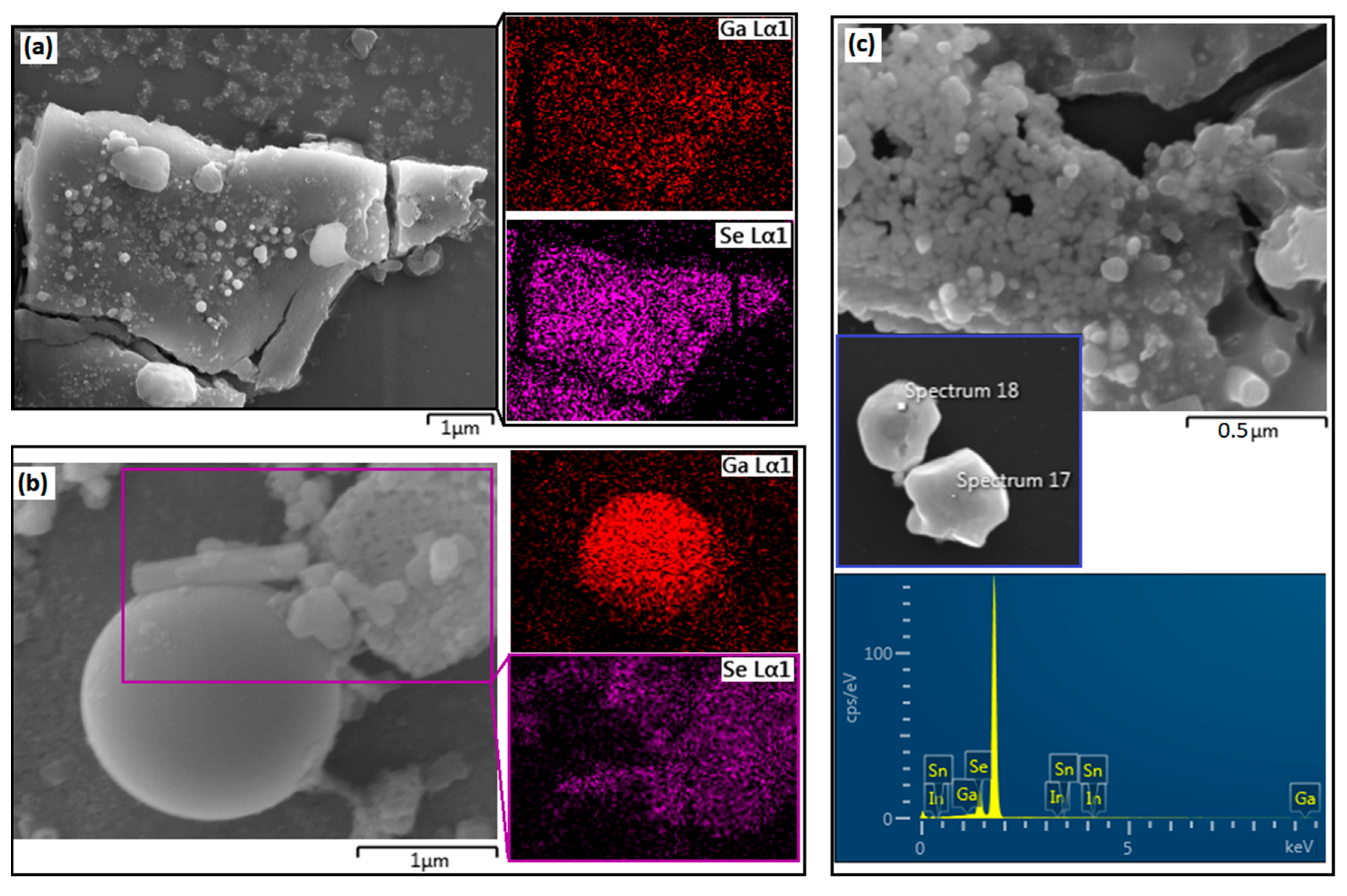
Figure 2.
(a) The SEM image accompanied by EDS analysis maps of Ga-Se nanosheet. (b) The SEM image showing the growth of Se-rich nanostructures on the surface of galinstan NPs accompanied by the EDS maps of nanostructures. (c) The Se nanoparticles grown individually during sonochemical reactions on the surface of galinstan NP.

Figure 3.
(a) The TEM image and corresponding SAED patterns of surface of galinstan NPs with Ag nanodomains. (b) The Raman and PL spectra of galinstan-Ag NPs. (c) The TEM image and corresponding SAED patterns of surface of galinstan NPs with Se nanodomains. (d) The Raman and PL spectra of galinstan-Se NPs. (e) The TEM image and corresponding SAED patterns of surface of galinstan NPs with Nb nanodomains. (f) The Raman and PL spectra of galinstan-Nb NPs.

Figure 4.
(a) The Ag 3d spectra of galinstan-Ag heterointerfaces. (b) The Ga 3d spectra of Ag 3d spectra of galinstan-Ag heterointerfaces. (c) The O 1s peak of galinstan-Ag heterointerfaces. (d) The Se 4d spectra of galinstan-Se heterointerfaces. (e) The Ga 3d spectra of galinstan-Ag heterointerfaces. (f) The O 1s peak of galinstan-Se heterointerfaces. (g) The Nb 3d spectra of galinstan-Nb heterointerfaces. (h) The Ga 3d spectra of galinstan-Se heterointerfaces. (i) The O 1s spectra of galinstan-Nb interfaces. (j) The VBM of hybrid 2D heterointerfaces.


Table 1.
The specifications of various types of synthesized Se-rich nanostructures.
| Shape | Dimension (μm) | Composition of Nanostructure Wt.% | Se Concentration in Solution (μmol/L) |
| 2D single-layered nanosheets | 1.0 < Length (L) < 100 0.05 < Thickness (D) < 2 | Se ≥ 30 20 < Ga < 50 | 0.2, 0.5 |
| 2D multi-layered nanosheets | 50 < L < 1000 0.5 < D < 10 | Se ≥ 40 20 < Ga < 40 | 0.2, 0.5 |
| 1D nanostructures | 100 < L < 700 50 < D < 100 | Se ≥ 90 | 0.1, 0.2 |
| 0D nanoparticles | 0.001 < D < 0.020 | Se ≥ 90 | 0.1, 0.2, 0.5 |
Disclaimer/Publisher’s Note: The statements, opinions and data contained in all publications are solely those of the individual author(s) and contributor(s) and not of MDPI and/or the editor(s). MDPI and/or the editor(s) disclaim responsibility for any injury to people or property resulting from any ideas, methods, instructions or products referred to in the content. |
© 2023 by the authors. Licensee MDPI, Basel, Switzerland. This article is an open access article distributed under the terms and conditions of the Creative Commons Attribution (CC BY) license (https://creativecommons.org/licenses/by/4.0/).
Share and Cite
MDPI and ACS Style
Karbalaei Akbari, M.; Siraj Lopa, N.; Zhuiykov, S. Crystalline Nanodomains at Multifunctional Two-Dimensional Liquid–Metal Hybrid Interfaces. Crystals 2023, 13, 604. https://doi.org/10.3390/cryst13040604
AMA Style
Karbalaei Akbari M, Siraj Lopa N, Zhuiykov S. Crystalline Nanodomains at Multifunctional Two-Dimensional Liquid–Metal Hybrid Interfaces. Crystals. 2023; 13(4):604. https://doi.org/10.3390/cryst13040604
Chicago/Turabian StyleKarbalaei Akbari, Mohammad, Nasrin Siraj Lopa, and Serge Zhuiykov. 2023. "Crystalline Nanodomains at Multifunctional Two-Dimensional Liquid–Metal Hybrid Interfaces" Crystals 13, no. 4: 604. https://doi.org/10.3390/cryst13040604
Note that from the first issue of 2016, this journal uses article numbers instead of page numbers. See further details here.