Communication

Efficient Activation and High Mobility of Ion-Implanted Silicon for Next-Generation GaN Devices

1
U.S. Naval Research Laboratory, Washington, DC 20375, USA
2
Virginia Polytechnic Institute and State University, Blacksburg, VA 24060, USA
*
Author to whom correspondence should be addressed.
Crystals 2023, 13(5), 736; https://doi.org/10.3390/cryst13050736
Submission received: 17 March 2023 / Revised: 21 April 2023 / Accepted: 25 April 2023 / Published: 27 April 2023
(This article belongs to the Special Issue Research in GaN-based Materials and Devices)

Abstract

:
Selective area doping via ion implantation is crucial to the implementation of most modern devices and the provision of reasonable device design latitude for optimization. Herein, we report highly effective silicon ion implant activation in GaN via Symmetrical Multicycle Rapid Thermal Annealing (SMRTA) at peak temperatures of 1450 to 1530 °C, producing a mobility of up to 137 cm2/Vs at 300K with a 57% activation efficiency for a 300 nm thick 1 × 1019 cm−3 box implant profile. Doping activation efficiency and mobility improved alongside peak annealing temperature, while the deleterious degradation of the as-grown material electrical properties was only evident at the highest temperatures. This demonstrates efficient dopant activation while simultaneously maintaining low levels of unintentional doping and thus a high blocking voltage potential of the drift layers for high-voltage, high-power devices. Furthermore, efficient activation with high mobility has been achieved with GaN on sapphire, which is known for having relatively high defect densities but also for offering significant commercial potential due to the availability of cheap, large-area, and robust substrates for devices.

1. Introduction

Gallium nitride materials and devices are critical to current and future communications and power electronics. The anticipated demand for faster data communication, power conversion devices for electromobility, and a myriad of additional applications has driven significant interest in obtaining efficient GaN devices with traditional topologies owing to their intrinsic potential with respect to their high breakdown fields, switching speed, power density, and efficiency [1,2,3,4,5,6,7]. These topologies inherently require spatially defined doping regimes, which are best implemented via ion implantation and annealing, the current industrial standard. While the material properties of GaN show great potential, this material’s inherent high-temperature instability precludes long anneals at standard-pressure, resulting in limited device topologies and necessitating novel solutions for spatially confined doping. To date, this has primarily been achieved via confined epitaxy or regrowth and etch methods. Inherently, these solutions introduce interfacial challenges resulting in reduced capabilities compared to a monolithic growth process [8].
The difficulty in achieving ion implant activation stems from the limited annealing temperatures available, namely, ca. 1000 °C, for long periods before decomposition. To achieve effective atomic mobility in order to remove implant-induced damage and activate dopants, temperatures must typically exceed 1300–1400 °C as this is ~2/3 of the melting point of GaN at 2200 °C. At these temperatures, GaN will decompose to its constituent elements without an excess nitrogen vapor pressure of several GPa [9], which is often termed ultra-high-pressure annealing (UHPA) [10,11,12]. This basic stabilization method proves effective when used with implanted devices and architectures tested on small samples [13,14,15]; however, when scaled up to the wafer scale, processing remains challenging or impossible depending on the temperature and pressure regime. While the limited activation of dopants, including devices, via rapid thermal-annealing (RTA) topologies in conjunction with capping moieties has been demonstrated previously [16,17,18], there is a dearth of data showing low compensation, high mobility, and high efficiency. Specifically, concerning silicon implant activation, demonstrations as early as 1995 exhibited low mobility and n-type conductivity [19], while improvements in the following decade made by various groups [20,21,22,23] demonstrated activation efficiencies/mobilities of up to 68%/~100 cm2/Vs at a 1 × 1015 cm−2 dose [21] and ~60%/240 cm2/Vs and 15%/112 cm2/Vs at 5 × 10¹⁷ and 1 × 1019 cm−3 donor concentrations, respectively [23].
In this study, we present the activation of a silicon ion implanted into GaN on sapphire, leading to results exceeding previously reported values while simultaneously maintaining the low doping of the adjacent, in-implanted regions via symmetric multicycle rapid thermal annealing (SMRTA). Such a process has shown previous success with respect to activating implanted Mg for p-type films [24,25,26,27], reducing contact resistance with an Si implant [28], and maintaining or improving undoped film quality [29,30].

2. Materials and Methods
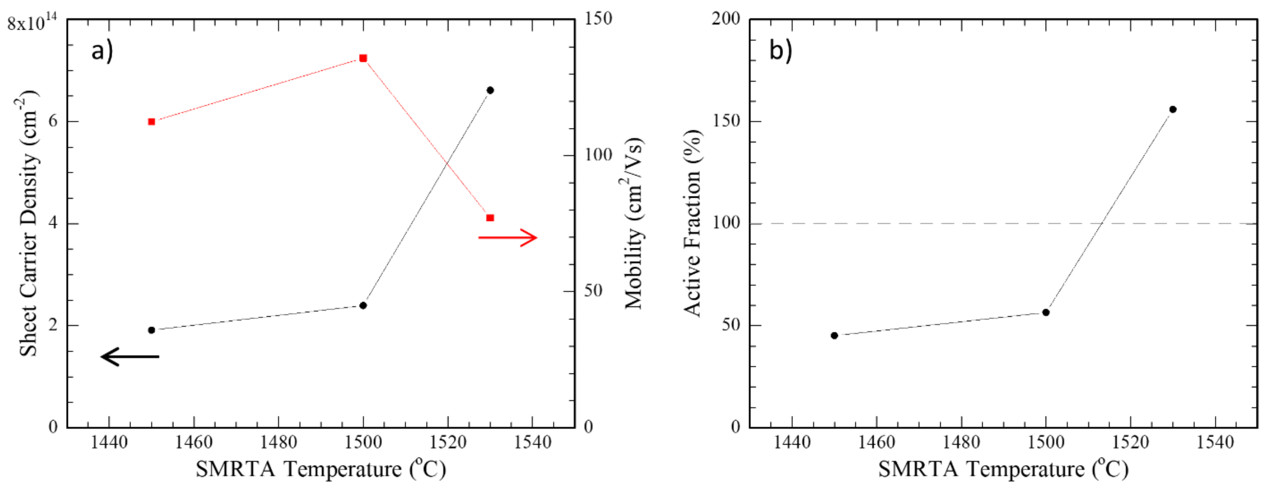
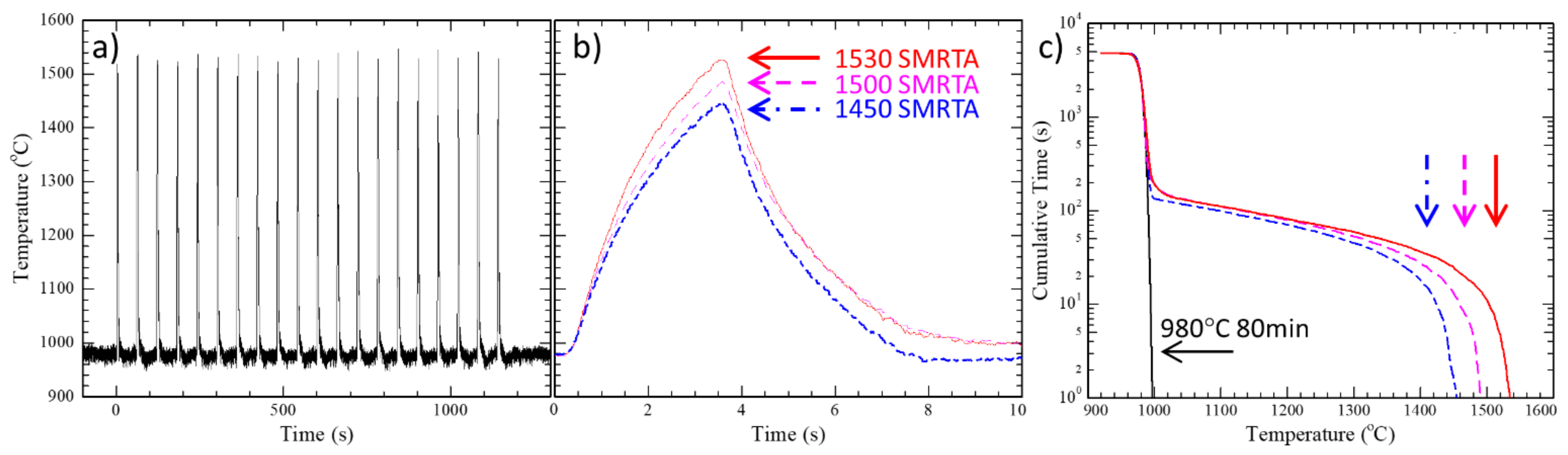
Unintentionally doped GaN was grown 2.2 μm thick on c-plane sapphire using a 25 nm AlN buffer layer. The growth temperature of the GaN was 1020 °C at a pressure of 200 Torr and a growth rate of 2.2 μm/h [31]. The GaN film was etched with 10 μm wide trenches approximately 1.5 μm deep via Ar/Cl RIE to isolate measurement structures and imprint sample identification markings. Samples were then coated with 30 nm of PECVD SiNx at 600 °C for protection during ion implantation and subsequently patterned using standard photolithography processes, utilizing 3 μm of photoresist to locally block the implant to produce Van derPauw structures and linear and circular transmission line measurements (TLMs). Silicon was implanted at 7 degrees and room temperature using energies ranging from 15 to 360 keV, as previously reported [32], to approximate a 1 × 1019 cm−3 box profile that was ~335 nm deep (at 5 × 1018 cm−3 concentration) with a surface concentration of 5 × 1019 cm−3 and thus facilitate electrical contact (as shown in Figure 1a). The implant total dose was 5 × 1014 cm−2, of which 4.24 × 1014 cm−2 was expected to reside in the GaN according to SRIM calculations, with the rest having remained in the implant cap. Previous SIMS measurements have shown very good agreement between SRIM and as-implanted dopant profiles. After implantation, samples were cleaned in heated Piranha solution and then concentrated HF solution to remove photoresist and implant cap. After cleaning, wafers were coated with a 200 nm PECVD SiNx anneal cap (n~1.99 via ellipsometry), diced into coupons, and annealed under various SMRTA conditions. Figure 1b shows the central region of sample 2A after dicing, and Figure 1c shows the same area after annealing at a peak temperature of 1500 °C. After annealing, the cap was removed in HF immediately before the electron beam evaporation of standard Ti/Al/Ni/Au contacts and measured as deposited.
Annealing and activation of implanted dopants were achieved via SMRTA consisting of a degree of moderate nitrogen overpressure of ~35 bar, the cap described above, and a three-step annealing process. The first step consisted of heating for a 30 min period at ~980 °C, wherein the GaN was thermodynamically stable, which was followed by 20 metastable high-temperature pulses separated by 60 s, and finally an additional 30 min period at 980 °C. Such a three-step process has been shown to be beneficial from a structural perspective [33]. Figure 2a shows a time–temperature profile of the high-temperature pulses for the nominal 1530 °C annealing phase. Each individual pulse remained above 1000 °C for less than 8 s and achieved up to 330 K/s heating and cooling rates, thereby highlighting the transient nature of this annealing process. Figure 2b shows a comparison of the average temperature pulses for the three peak temperatures, highlighting the similar ramp rates and timescale while presenting differing peak absolute temperatures from 1450–1530 °C. Figure 2c shows a plot of the cumulative time at a given temperature on semi-log scales achieved for these annealing schemes for comparative purposes. An additional sample was annealed at 980 °C for 80 min as a baseline; however, it was too resistive to measure.
Contact and GaN sheet resistance was first characterized via linear TLMs with pad separations ranging from 4 to 80 μm using a Keithly 4200SCS SMU. Figure 3a shows ohmic contacts of TLM pads, while Figure 3b shows the well-behaved nature of contacts in the implanted region after the 1500 °C SMRTA. Hall effect was measured on a Lakeshore Cryotronics system with M90 Fast Hall across ±0.95 T field at 300 K. Contacts were determined to be ohmic as deposited, with specific contact resistances of 1.6 to 6.6 × 10⁻⁵ Ω-cm2, and TLM-extracted sheet resistances exhibited good agreement with measurements of Van der Pauw structures during AC Hall effect testing. No contact-alloying anneal was utilized and no trend was observed in contact resistance as a function of the SMRTA peak temperature.

3. Results

Hall effect data were acquired at room temperature with the sheet resistance measured at zero field and at each field point to improve statistics and verify that the probes did not shift. The magnetoresistive effects observed were small compared to all other variations due to probe contact. Due to asymmetries in layout or contacts, the hall voltage was found to have a small offset (typically < 0.1 μV). This offset was circumvented by determining the sheet carrier density directly from dVH/dB and then mobility from the sheet resistance and sheet density. Consequently, the resultant values were consistent and uniform across multiple Hall structures on a single sample. Figure 4a shows the resultant sheet carrier density and mobility for the implanted regions, for which both quantities are shown to improve alongside an increasing annealing temperature up to 1500 °C, yielding 2.4 × 1014 cm−2 and 137 cm2/Vs. Above 1500 °C, a marked degradation of the UID film and excess activation beyond the implant dose were noted. Figure 4b shows the effective activation efficiency obtained by dividing the sheet carrier density by the implant dose (4.24 × 1014 cm−2), showing a value of 57% after the 1500 °C SMRTA and 156% after the 1530 °C SMRTA, further exemplifying the degradation after annealing at 1530 °C. Judging by the activation efficiency at 1500 °C and the intended 1 × 1019 cm−3 box implant profile, the majority of the box should have a carrier density near ~6 × 1018 cm−3. Given the degree of mobility under this condition, this suggests a compensation ratio of ~0.45 [34], which is in reasonable agreement with unity minus the observed sheet activation efficiency. In comparison, the SIMS data of similar as-grown films indicate an unintentional impurity inclusion of [Si] < 1 × 10¹⁶ and [C]~[O] = 5 × 1016 cm−3. The significant increase in mobility and activation efficiency relative to the previously reported results further confirms the resultant high quality of the annealed material and the low level of compensation developed, indicating the effectiveness of SMRTA over traditional RTA-style anneals. This effectiveness likely stems from the higher temperatures and long durations enabled via the SMRTA process, which result in reduced residual defect concentrations; however, the specific mechanisms and limiting defect species require further investigation.
While improved mobility and activation efficiency are useful for devices, care must be taken to ensure that there are no significant alterations to unintentionally doped or resistive films, which must hold large fields when implemented in devices. Figure 5 shows the measured sheet carrier density and implied volumetric carrier density in the in-implanted Van derPauw structures immediately adjacent to the implanted structures. While the carrier density increases from the low 15 s to the mid 17 s, we note that carrier densities of 1−2 × 1016 cm−3 (condition after 1500 °C SMRTA) are sufficient for 1.5 kV class devices and have separately been fabricated in-house on bulk GaN [35], yielding 1.3 kV PiN diodes. This demonstrates the compatibility of these implant and annealing processes for the fabrication of future two-terminal (e.g., JBS and MPS diodes) or three-terminal (e.g., VDMOS, CAVET, etc.) devices with traditional device topologies, while further optimization of the anneal conditions can produce improved UID and implant performance.

4. Conclusions

The initial testing of a silicon ion implanted into GaN on sapphire has shown a peak in mobility at 137 cm2/Vs with 57% activation efficiency after the a 1500 °C peak temperature SMRTA resulting in an estimated 45% compensation ratio. Above this temperature, significant degradation was observed. Unimplanted regions that were directly adjacent showed resultant carrier densities of 1.8 × 10¹⁶, which is sufficient for ~1.5 kV class devices under these conditions despite the lack of optimization of annealing temperature or pulse structure, co-implantation for vacancy reduction, or implant condition effects, suggesting that readily accessible improvements are possible and thus applicable to higher-voltage devices. Furthermore, the demonstration of effective, selective area, n-type implant activation for a 1.5 kV class material on commercially scalable and inexpensive GaN on sapphire provides a facile route toward rapid integration for future GaN devices.

Author Contributions

A.G.J. was responsible for the project’s coordination, material processing and annealing, data acquisition, and analysis and was the lead writer of the manuscript. B.N.F. was responsible for project management, inception, funding, and the annealing procedure’s conception. J.A.S. was responsible for data acquisition and material processing. M.J.T. was responsible for guidance and mentoring, J.K.H. grew the GaN films. K.D.H. and T.J.A. were responsible for project management. All authors contributed equally to this work and manuscript. All authors have read and agreed to the published version of the manuscript.

Funding

Work conducted at the U.S. Naval Research Laboratory was supported by the Office of Naval Research. J.A.S. is partially supported by the High-Density Integration industry consortium.

Data Availability Statement

Data will be made available upon reasonable request.

Acknowledgments

Research conducted at NRL was supported by the Office of Naval Research. The authors acknowledge the NRL Institute for Nanoscience (A. Boyd, D. St. Amand, and W. Spratt) for fabrication support. J.A.S. gratefully acknowledges the support provided by the High-Density Integration industry consortium.

Conflicts of Interest

The authors declare no conflict of interest.

References

  1. Pengelly, R.S.; Wood, S.M.; Milligan, J.W.; Sheppard, S.T.; Pribble, W.L. A review of GaN on SiC high electron-mobility power transistors and MMICs. IEEE Trans. Microw. Theory Tech. 2012, 60, 1764–1783. [Google Scholar] [CrossRef]
  2. Wu, Y.F.; Gritters, J.; Shen, L.; Smith, R.P.; Swenson, B. kV-Class GaN-on-Si HEMTs enabling 99% efficiency converter at 800 V and 100 kHz. IEEE Trans. Power Electron. 2014, 29, 2634–2637. [Google Scholar] [CrossRef]
  3. Chen, K.J.; Häberlen, O.; Lidow, A.; Tsai, C.L.; Ueda, T.; Uemoto, Y.; Wu, Y. GaN-on-Si power technology: Devices and applications. IEEE Trans. Electron. Devices 2017, 64, 779–795. [Google Scholar] [CrossRef]
  4. DenBaars, S.P.; Feezell, D.; Kelchner, K.; Pimputkar, S.; Pan, C.-C.; Yen, C.-C.; Tanaka, S.; Zhao, Y.; Pfaff, N.; Farrell, R.; et al. Development of gallium-nitride-based light-emitting diodes (LEDs) and laser diodes for energy-efficient lighting and displays. Acta Mater. 2013, 61, 945–951. [Google Scholar] [CrossRef]
  5. Nie, H.; Diduck, Q.; Alvarez, B.; Edwards, A.P.; Kayes, B.M.; Zhang, M.; Ye, G.; Prunty, T.; Bour, D.; Kizilyalli, I.C. 1.5-kV and 2.2-mΩ-cm2 Vertical GaN Transistors on Bulk-GaN Substrates. IEEE Electron Device Lett. 2014, 35, 939–941. [Google Scholar] [CrossRef]
  6. Sun, M.; Zhang, Y.; Gao, X.; Palacios, T. High-performance GaN vertical fin power transistors on bulk GaN substrates. IEEE Electron Device Lett. 2017, 38, 509–512. [Google Scholar] [CrossRef]
  7. Zhang, Y.; Liu, Z.; Tadjer, M.J.; Sun, M.; Piedra, D.; Hatem, C.; Anderson, T.J.; Luna, L.E.; Nath, A.; Koehler, A.D.; et al. Vertical GaN junction barrier schottky rectifiers by selective ion implantation. IEEE Electron Device Lett. 2017, 38, 1097–1100. [Google Scholar] [CrossRef]
  8. Chang, A.S.; Li, B.; Wang, S.; Frisone, S.; Goldman, R.S.; Han, J.; Lauhon, L.J. Unveiling the influence of selective-area-regrowth interfaces on local electronic properties of GaN p-n junctions for efficient power devices. Nano Energy 2022, 102, 107689. [Google Scholar] [CrossRef]
  9. Unland, J.; Onderka, B.; Davydov, A.; Schmid-Fetzer, R. Thermodynamics and phase stability in the Ga–N system. J. Cryst. Growth 2003, 256, 33–51. [Google Scholar] [CrossRef]
  10. Unland, J.; Onderka, B.; Davydov, A.; Schmid-Fetzer, R. Recent progress of Mg-ion implantation and thermal activation process for p-doping in GaN (conference presentation). In Proceedings of the Gallium Nitride Materials and Devices XIV, San Francisco, CA, USA, 13 March 2019; p. 30. [Google Scholar]
  11. Sierakowski, K.; Jakiela, R.; Lucznik, B.; Kwiatkowski, P.; Iwinska, M.; Turek, M.; Sakurai, H.; Kachi, T.; Bockowski, M. High pressure processing of ion implanted gan. Electron 2020, 9, 1380. [Google Scholar] [CrossRef]
  12. Sakurai, H.; Narita, T.; Hirukawa, K.; Yamada, S.; Koura, A.; Kataoka, K.; Horita, M.; Ikarashi, N.; Bockowski, M.; Suda, J.; et al. Impacts of high temperature annealing above 1400 °C under N2 overpressure to activate acceptors in Mg-implanted GaN. In Proceedings of the 2020 32nd International Symposium on Power Semiconductor Devices and ICs (ISPSD), Vienna, Austria, 13–18 September 2020; pp. 321–324. [Google Scholar]
  13. Narita, T.; Yoshida, H.; Tomita, K.; Kataoka, K.; Sakurai, H.; Horita, M.; Bockowski, M.; Ikarashi, N.; Suda, J.; Kachi, T.; et al. Progress on and challenges of p-type formation for GaN power devices. J. Appl. Phys. 2020, 128, 090901. [Google Scholar] [CrossRef]
  14. Matys, M.; Ishida, T.; Nam, K.P.; Sakurai, H.; Kataoka, K.; Narita, T.; Uesugi, T.; Bockowski, M.; Nishimura, T.; Suda, J.; et al. Design and demonstration of nearly-ideal edge termination for GaN p-n junction using Mg-implanted field limiting rings. Appl. Phys. Express 2021, 14, 074002. [Google Scholar] [CrossRef]
  15. Matys, M.; Ishida, T.; Nam, K.P.; Sakurai, H.; Narita, T.; Uesugi, T.; Bockowski, M.; Suda, J.; Kachi, T. Mg-implanted bevel edge termination structure for GaN power device applications. Appl. Phys. Lett. 2021, 118, 3–8. [Google Scholar] [CrossRef]
  16. Irokawa, Y.; Kim, J.; Ren, F.; Baik, K.; Gila, B.; Abernathy, C.; Pearton, S.; Pan, C.-C.; Chen, G.-T.; Chyi, J.-I.; et al. Si+ ion implanted MPS bulk GaN diodes. Solid State Electron. 2004, 48, 827–830. [Google Scholar] [CrossRef]
  17. Yoshino, M.; Ando, Y.; Deki, M.; Toyabe, T.; Kuriyama, K.; Honda, Y.; Nishimura, T.; Amano, H.; Kachi, T.; Nakamura, T. Fully ion implanted normally-off GaN DMOSFETs with ALD-Al 2 O 3 gate dielectrics. Materials 2019, 12, 689. [Google Scholar] [CrossRef] [PubMed]
  18. Ito, K.; Tomita, K.; Kikuta, D.; Horita, M.; Narita, T. Analysis of channel mobility in GaN-based metal-oxide-semiconductor field-effect transistors. J. Appl. Phys. 2021, 129, 084502. [Google Scholar] [CrossRef]
  19. Tan, H.H.; Williams, J.S.; Zou, J.; Cockayne, D.J.H.; Pearton, S.J.; Stall, R.A. Damage to epitaxial GaN layers by silicon implantation. Appl. Phys. Lett. 1996, 69, 2364–2366. [Google Scholar] [CrossRef]
  20. Dupuis, R.D.; Eiting, C.J.; Grudowski, P.A.; Hsia, H.; Tang, Z.; Becher, D.; Kuo, H.; Stillman, G.E.; Feng, M. Activation of silicon ion-implanted gallium nitride by furnace annealing. J. Electron. Mater. 1999, 28, 319–324. [Google Scholar]
  21. Nakano, Y.; Jimbo, T. Co-implantation of Si+N into GaN for n -type doping. J. Appl. Phys. 2002, 92, 3815–3819. [Google Scholar] [CrossRef]
  22. Nakano, Y.; Kachi, T.; Jimbo, T. N-type implantation doping of GaN. Mater. Sci. Semicond. Process. 2003, 6, 515–517. [Google Scholar] [CrossRef]
  23. Hager, C.E.; Jones, K.A.; Derenge, M.A.; Zheleva, T.S. Activation of ion implanted Si in GaN using a dual AlN annealing cap. J. Appl. Phys. 2009, 105, 033713. [Google Scholar] [CrossRef]
  24. Greenlee, J.D.; Feigelson, B.N.; Anderson, T.J.; Tadjer, M.J.; Hite, J.K.; Mastro, M.A.; Eddy, C.R.J.; Hobart, K.D.; Kub, F.J. Multicycle rapid thermal annealing optimization of Mg-implanted GaN: Evolution of surface, optical, and structural properties. J. Appl. Phys. 2014, 116, 063502. [Google Scholar] [CrossRef]
  25. Jacobs, A.G.; Feigelson, B.N.; Hite, J.K.; Gorsak, C.A.; Luna, L.E.; Anderson, T.J.; Kub, F.J. Polarity dependent implanted p-type dopant activation in GaN. Jpn. J. Appl. Phys. 2019, 58, SCCD07. [Google Scholar] [CrossRef]
  26. Jacobs, A.G.; Feigelson, B.N.; Hite, J.K.; Gorsak, C.A.; Luna, L.E.; Anderson, T.J.; Kub, F.J. Role of capping material and GaN polarity on Mg ion implantation activation. Phys. Status Solidi Appl. Mater. Sci. 2019, 217, 1900789. [Google Scholar] [CrossRef]
  27. Ebrish, M.A.; Anderson, T.J.; Jacobs, A.G.; Gallagher, J.C.; Hite, J.K.; Mastro, M.A.; Feigelson, B.N.; Wang, Y.; Liao, M.; Goorsky, M.; et al. Process optimization for selective area doping of GaN by ion implantation. J. Electron. Mater. 2021, 50, 4642–4649. [Google Scholar] [CrossRef]
  28. Gallagher, J.C.; Kub, F.J.; Anderson, T.J.; Koehler, A.D.; Foster, G.M.; Jacobs, A.G.; Feigelson, B.N.; Mastro, M.A.; Hite, J.K.; Hobart, K.D. Reduced contact resistance in GaN using selective area Si ion implantation. IEEE Trans. Semicond. Manuf. 2019, 32, 478–482. [Google Scholar] [CrossRef]
  29. Gallagher, J.C.; Anderson, T.J.; Koehler, A.D.; Foster, G.M.; Jacobs, A.G.; Feigelson, B.N.; Mastro, M.M.; Hite, J.K.; Hobart, K.D. Activation of ion implanted Si in semi-insulating C-doped GaN by high pressure annealing for photoconductive semiconductor switch (PCSS) applications. In Proceedings of the CS MANTECH 2019–2019 International Conference on Compound Semiconductor Manufacturing Technology, Digest of Papers, Minneapolis, MN, USA, 29 April–2 May 2019. [Google Scholar]
  30. Anderson, T.; Gallagher, J.; Luna, L.; Koehler, A.; Jacobs, A.; Xie, J.; Beam, E.; Hobart, K.; Feigelson, B. Effect of high temperature, high pressure annealing on GaN drift layers for vertical power devices. J. Cryst. Growth 2018, 499, 35–39. [Google Scholar] [CrossRef]
  31. Hite, J.; Anderson, T.; Luna, L.; Gallagher, J.; Mastro, M.; Freitas, J.; Eddy, C. Influence of HVPE substrates on homoepitaxy of GaN grown by MOCVD. J. Cryst. Growth 2018, 498, 352–356. [Google Scholar] [CrossRef]
  32. Jacobs, A.G.; Spencer, J.A.; Hite, J.K.; Hobart, K.D.; Anderson, T.J.; Feigelson, B.N. Novel Co-doping Moiety to Achieve Enhanced P-type doping in GaN by Ion Implantation. Phys. Status Solidi Appl. Mater. Sci. 2023. [Google Scholar] [CrossRef]
  33. Greenlee, J.D.; Feigelson, B.; Anderson, T.J.; Hite, J.K.; Hobart, K.D.; Kub, F.J. From MRTA to SMRTA: Improvements in activating implanted dopants in GaN. ECS Trans. 2015, 69, 97–102. [Google Scholar] [CrossRef]
  34. Chin, V.W.L.; Tansley, T.L.; Osotchan, T. Electron mobilities in gallium, indium, and aluminum nitrides. J. Appl. Phys. 1994, 75, 7365–7372. [Google Scholar] [CrossRef]
  35. Pandey, P.; Nelson, T.M.; Collings, W.M.; Hontz, M.R.; Georgiev, D.G.; Koehler, A.D.; Anderson, T.J.; Gallagher, J.C.; Foster, G.M.; Jacobs, A.; et al. A simple edge termination design for vertical GaN P-N diodes. Trans. Electron Devices 2021, 69, 5096–5103. [Google Scholar] [CrossRef]
Figure 1. (a) SRIM calculation of dopant profile in GaN with 30 nm SiNx cap, where 0 nm denotes SiNx:GaN interface on linear (solid black line) and log (dashed red line). (b) Nomarski image after implantation, wherein damage is visible as darkened regions, and (c) Nomarski image after annealing showing damage recovery and unchanged surface.
Crystals 13 00736 g001
Figure 2. (a) Observed temperature profile of SMRTA pulses during 1530 °C anneal. To ensure a greater focus on pulses, preceding and subsequent static annealing steps at ~980 °C are not shown. (b) Average of all 20 pulses for each SMRTA annea and (c) cumulative time duration at or above the indicated temperature for each SMRTA anneal and an 80 min anneal at 980 °C.
Crystals 13 00736 g002
Figure 3. TLM results with (a) increasing gap showing linear contacts under all conditions (dashed and solid lines are adjacent test structures) and (b) exhibiting linearity across all gaps, showing GaN acting as typical resistor after 1500 °C SMRTA, for which Rs ~160 Ω/□ and RC,sp ~4 × 10⁻⁴ Ω-cm2 were observed.
Crystals 13 00736 g003
Figure 4. (a) Implanted GaN sheet carrier density (black circles, left axis) and mobility (red squares, right axis) and (b) resultant activation efficiency as a function of peak annealing temperature.
Crystals 13 00736 g004
Figure 5. Un-implanted, unintentionally doped GaN carrier concentration (sheet—left axis; volumetric—right axis) after SMRTA annealing as a function of peak annealing temperature.
Crystals 13 00736 g005
Disclaimer/Publisher’s Note: The statements, opinions and data contained in all publications are solely those of the individual author(s) and contributor(s) and not of MDPI and/or the editor(s). MDPI and/or the editor(s) disclaim responsibility for any injury to people or property resulting from any ideas, methods, instructions or products referred to in the content.

