
Influence of Deposition Time on Structural, Morphological, and Optical Properties of CdS Thin Films Grown by Low-Cost Chemical Bath Deposition
 ,
,
Abstract
:1. Introduction
2. Materials and Methods
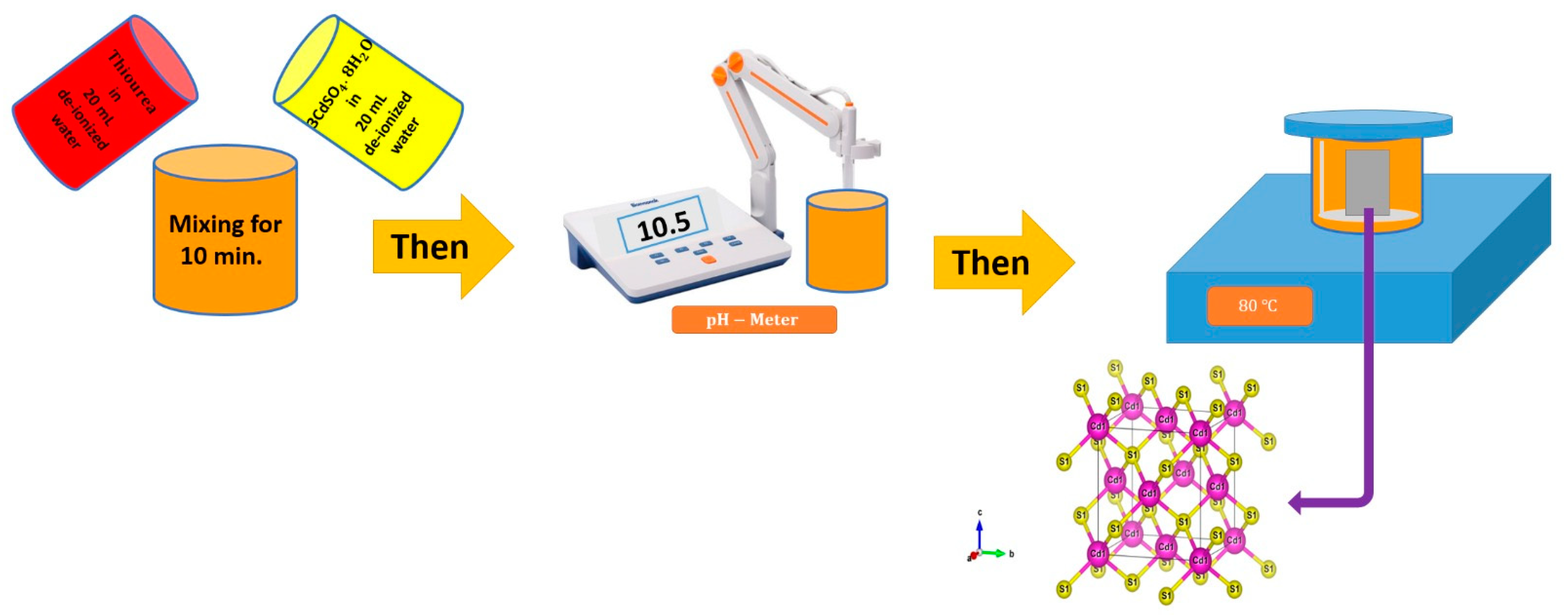
2.1. Materials
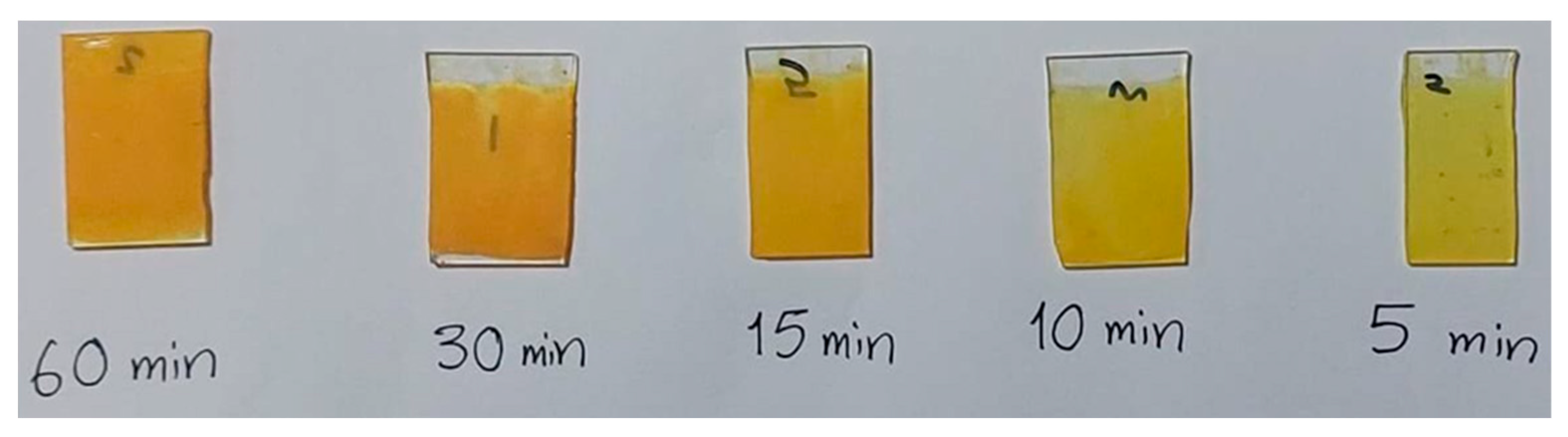
2.2. Sample Synthesis
3. Results and Discussion
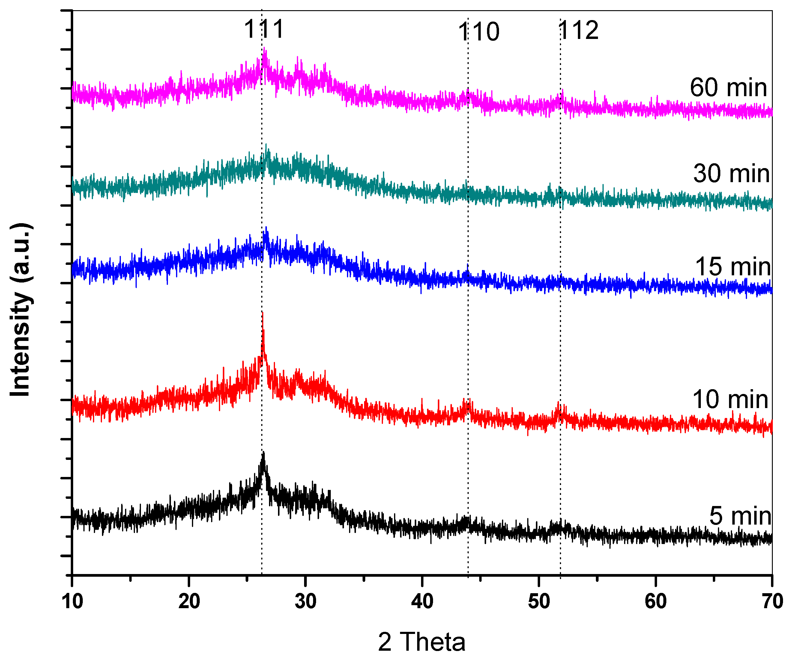
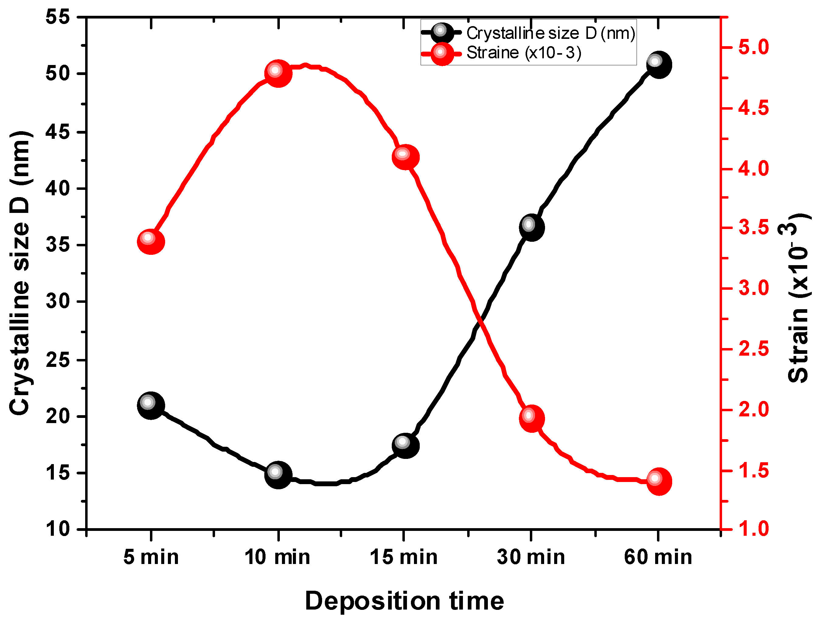
3.1. Analysis of Structural Properties
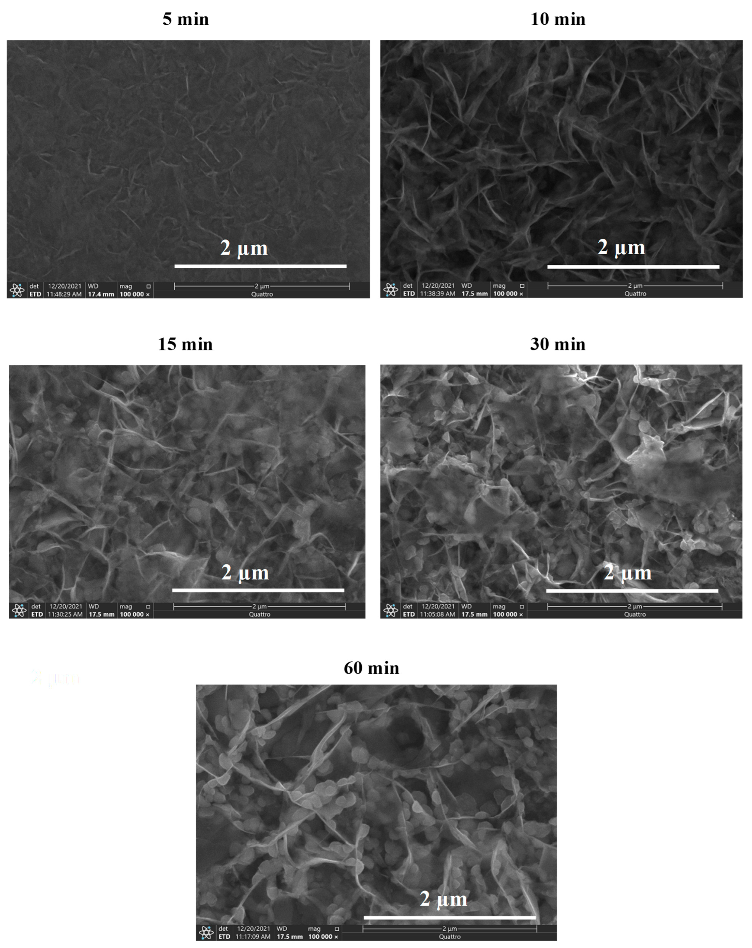
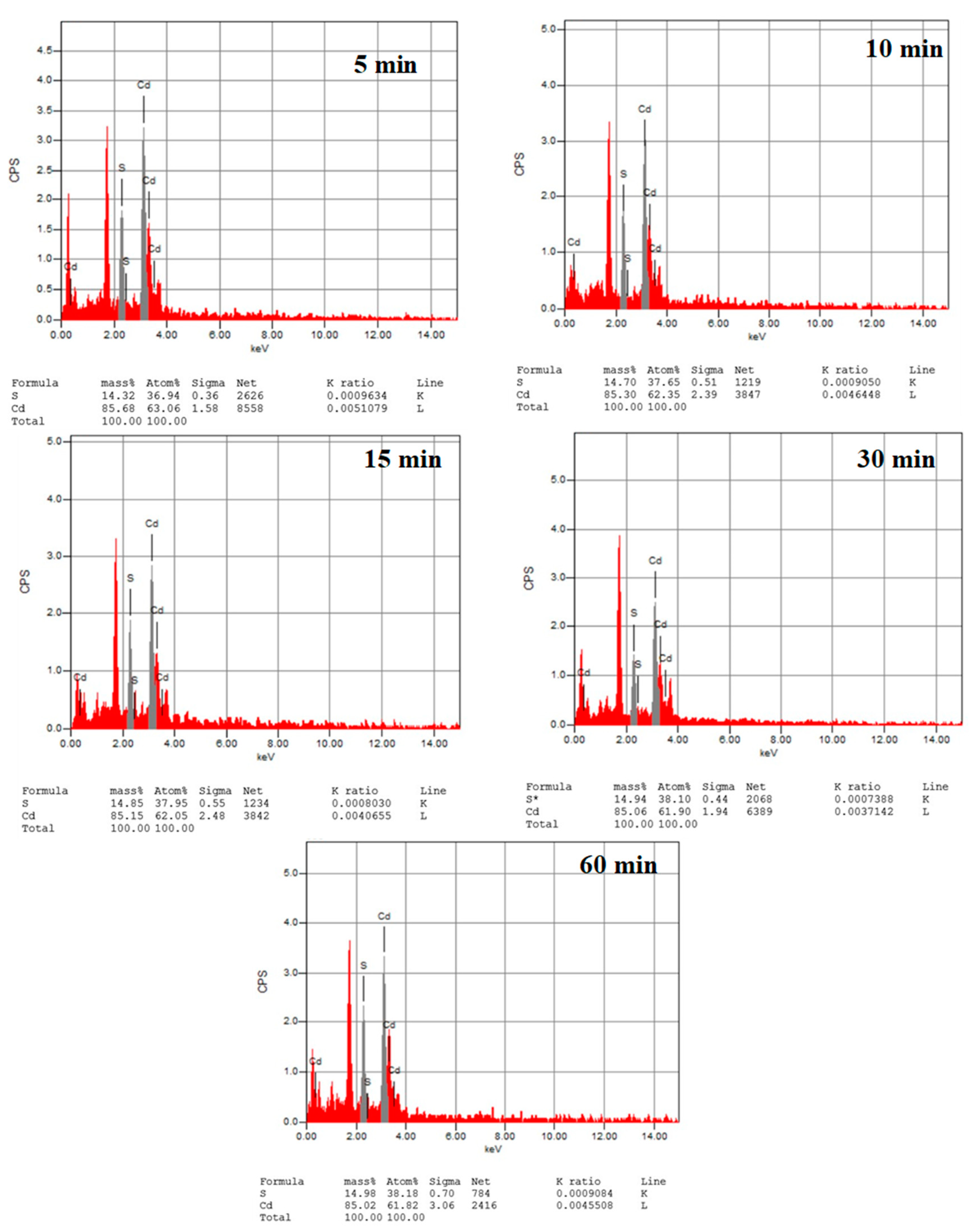
3.2. SEM Analysis
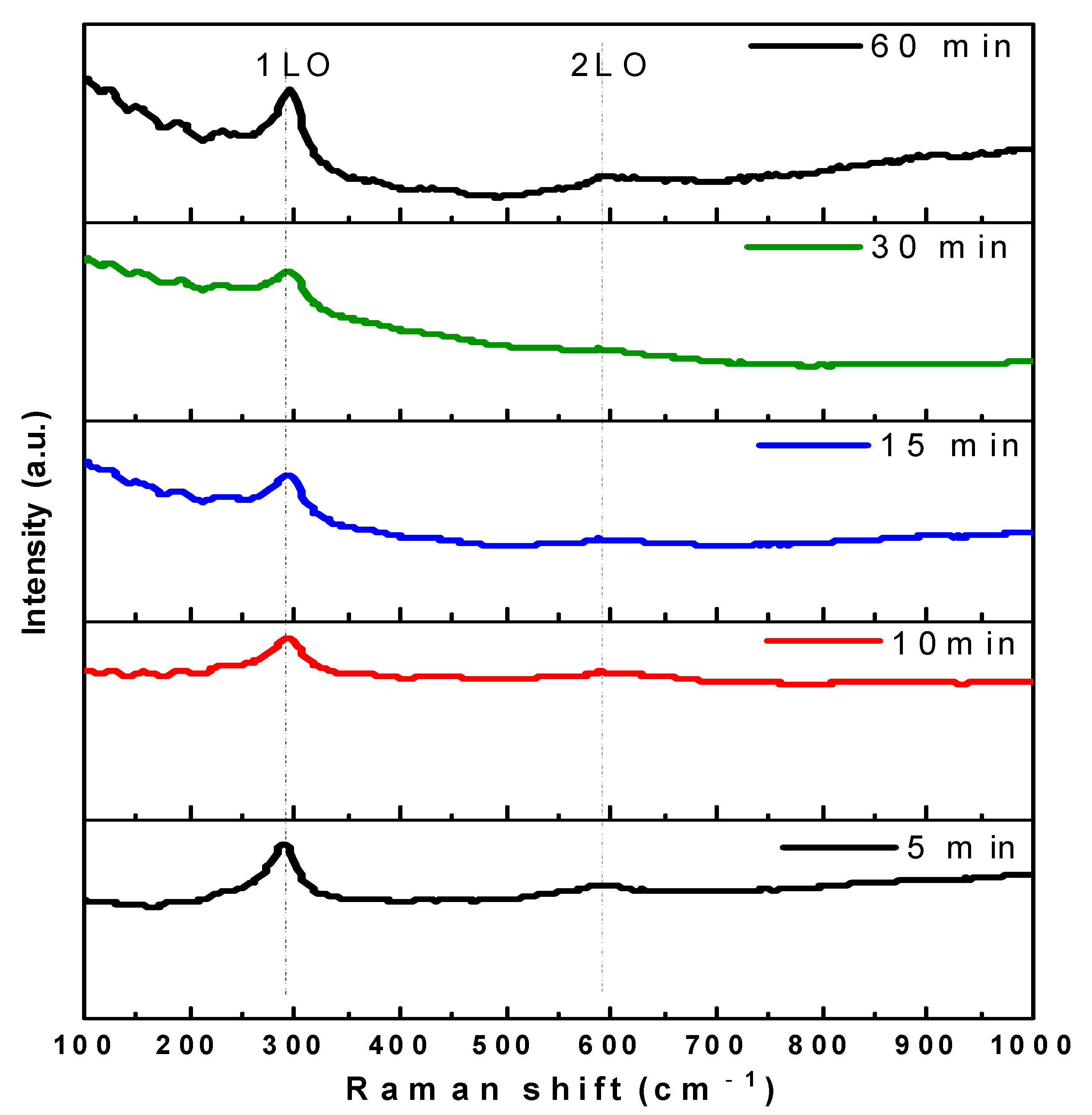
3.3. Raman Analysis
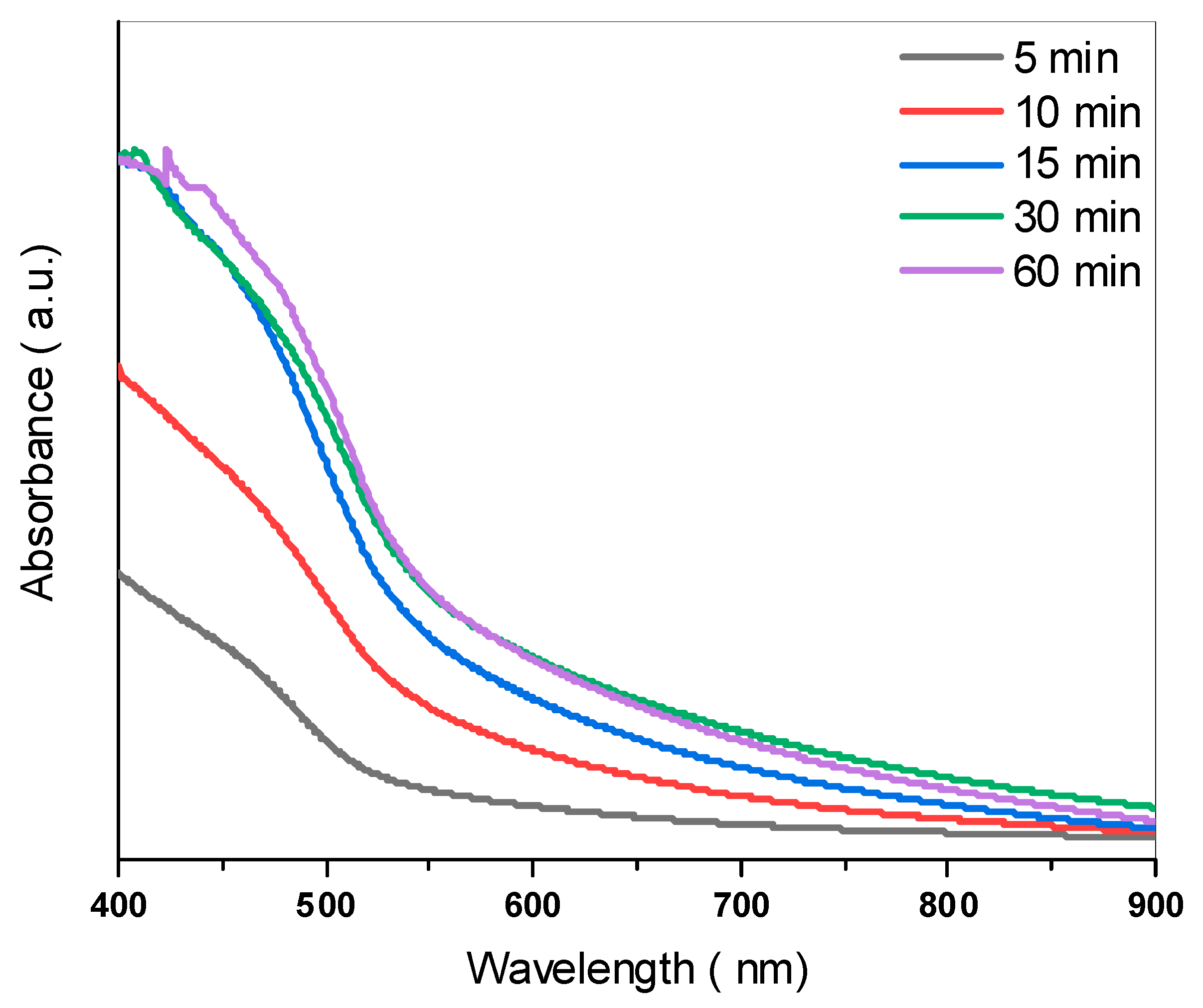
3.4. Optical Properties
3.5. PL Studies
4. Conclusions
Supplementary Materials
Author Contributions
Funding
Data Availability Statement
Conflicts of Interest
References
- Ashok, A.; Regmi, G.; Romero-Núñez, A.; Solis-López, M.; Velumani, S.; Castaneda, H. Comparative studies of CdS thin films by chemical bath deposition techniques as a buffer layer for solar cell applications. J. Mater. Sci. Mater. Electron. 2020, 31, 7499–7518. [Google Scholar] [CrossRef]
- Abou-Ras, D.; Kostorz, G.; Romeo, A.; Rudmann, D.; Tiwari, A. Structural and chemical investigations of CBD-and PVD-CdS buffer layers and interfaces in Cu (In, Ga) Se2-based thin film solar cells. Thin Solid Film. 2005, 480, 118–123. [Google Scholar] [CrossRef]
- Rahman, M.; Hossain, J.; Kuddus, A.; Tabassum, S.; Rubel, M.H.; Shirai, H.; Ismail, A.B.M. A novel synthesis and characterization of transparent CdS thin films for CdTe/CdS solar cells. Appl. Phys. A 2020, 126, 145. [Google Scholar] [CrossRef]
- Lokhande, C.; Ennaoui, A.; Patil, P.; Giersig, M.; Muller, M.; Diesner, K.; Tributsch, H. Process and characterisation of chemical bath deposited manganese sulphide (MnS) thin films. Thin Solid Film. 1998, 330, 70–75. [Google Scholar] [CrossRef]
- Sinha, T.; Lilhare, D.; Khare, A. Temperature-dependent structural, morphological and optical properties of chemical bath-deposited CdS films. Rare Met. 2021, 40, 701–707. [Google Scholar] [CrossRef]
- Ichimura, M.; Goto, F.; Arai, E. Structural and optical characterization of CdS films grown by photochemical deposition. J. Appl. Phys. 1999, 85, 7411–7417. [Google Scholar] [CrossRef]
- Sathish, M.; Viswanath, R. Photocatalytic generation of hydrogen over mesoporous CdS nanoparticle: Effect of particle size. noble metal and support. Catal. Today 2007, 129, 421–427. [Google Scholar] [CrossRef]
- Ouachtari, F.; Rmili, A.; Elidrissi, B.; Bouaoud, A.; Erguig, H.; Elies, P. Influence of bath temperature, deposition time and S/Cd ratio on the structure, surface morphology, chemical composition and optical properties of CdS thin films elaborated by chemical bath deposition. J. Mod. Phys. 2011, 2011, 1073–1082. [Google Scholar] [CrossRef]
- Kumar, A.; Pednekar, D.; Mukherjee, S.; Choubey, R.K. Effect of deposition time and complexing agents on hierarchical nanoflake-structured CdS thin films. J. Mater. Sci. Mater. Electron. 2020, 31, 17055–17066. [Google Scholar] [CrossRef]
- Abdelfatah, M.; Salah, H.Y.; El-Henawey, M.I.; Oraby, A.H.; El-Shaer, A.; Ismail, W. Insight into Co concentrations effect on the structural, optical, and photoelectrochemical properties of ZnO rod arrays for optoelectronic applications. J. Alloys Compd. 2021, 873, 159875. [Google Scholar] [CrossRef]
- Salah, H.; Mahmoud, K.; Ismail, W.; El-Shaer, A.; Oraby, A.; Abdelfatah, M.; EL-Henawey, M. Influence of Nickel Concentration on the Microstructure, Optical, Electrical, and Photoelectrochemical Properties of ZnO Nanorods Synthesized by Hydrothermal Method. J. Electron. Mater. 2022, 51, 910–920. [Google Scholar] [CrossRef]
- Salem, S.M.; Deraz, N.M.; Saleh, H.A. Fabrication and characterization of chemically deposited copper–manganese sulfide thin films. Appl. Phys. A 2020, 126, 700. [Google Scholar] [CrossRef]
- Kwon, J.-H.; Ahn, J.-S.; Yang, H. Chemical bath deposition of CdS channel layer for fabrication of low temperature-processed thin-film-transistors. Curr. Appl. Phys. 2013, 13, 84–89. [Google Scholar] [CrossRef]
- Lee, J. Raman scattering and photoluminescence analysis of B-doped CdS thin films. Thin Solid Film. 2004, 451, 170–174. [Google Scholar] [CrossRef]
- Shen, X.-P.; Yuan, A.-H.; Wang, F.; Hong, J.-M.; Xu, Z. Fabrication of well-aligned CdS nanotubes by CVD-template method. Solid State Commun. 2005, 133, 19–22. [Google Scholar] [CrossRef]
- Khan, Z.; Shkir, M.; Ganesh, V.; AlFaify, S.; Yahia, I.; Zahran, H. Linear and nonlinear optics of CBD grown nanocrystalline F doped CdS thin films for optoelectronic applications: An effect of thickness. J. Electron. Mater. 2018, 47, 5386–5395. [Google Scholar] [CrossRef]
- Rondiya, S.; Rokade, A.; Gabhale, B.; Pandharkar, S.; Chaudhari, M.; Date, A.; Chaudhary, M.; Pathan, H.; Jadkar, S. Effect of bath temperature on optical and morphology properties of CdS thin films grown by chemical bath deposition. Energy Procedia 2017, 110, 202–209. [Google Scholar] [CrossRef]
- Khan, Z.R.; Shkir, M.; Alshammari, A.S.; Ganesh, V.; AlFaify, S.; Gandouzi, M. Structural, linear and third order nonlinear optical properties of sol-gel grown Ag-CdS nanocrystalline thin films. J. Electron. Mater. 2019, 48, 1122–1132. [Google Scholar] [CrossRef]
- Tauc, J. Optical Properties of Solids 22; Abeles, F., Ed.; North Holland Pub: Amsterdam, The Netherlands, 1970. [Google Scholar]
- Abel, S.; Tesfaye, J.L.; Gudata, L.; Lamessa, F.; Shanmugam, R.; Dwarampudi, L.P.; Nagaprasad, N.; Krishnaraj, R. Investigating the Influence of Bath Temperature on the Chemical Bath Deposition of Nanosynthesized Lead Selenide Thin Films for Photovoltaic Application. J. Nanomater. 2022, 2022, 3108506. [Google Scholar] [CrossRef]
- Priya, N.S.; Kamala, S.S.P.; Anbarasu, V.; Azhagan, S.A.; Saravanakumar, R. Characterization of CdS thin films and nanoparticles by a simple chemical bath technique. Mater. Lett. 2018, 220, 161–164. [Google Scholar] [CrossRef]
- Khot, K.V.; Mali, S.S.; Pawar, N.B.; Kharade, R.R.; Mane, R.M.; Kondalkar, V.V.; Patil, P.B.; Patil, P.S.; Hong, C.K.; Kim, J.H. Development of nanocoral-like Cd (SSe) thin films using an arrested precipitation technique and their application. New J. Chem. 2014, 38, 5964–5974. [Google Scholar] [CrossRef]
- Ghazi, M.; Izadifard, M.; Ghodsi, F.E.; Yuonesi, M. Studying Mn-and Ni-doped ZnO thin films synthesized by the sol–gel method. J. Supercond. Nov. Magn. 2012, 25, 101–108. [Google Scholar] [CrossRef]
- Mazón-Montijo, D.A.; Sotelo-Lerma, M.; Quevedo-López, M.; El-Bouanani, M.; Alshareef, H.N.; Espinoza-Beltrán, F.J.; Ramírez-Bon, R. Morphological and chemical study of the initial growth of CdS thin films deposited using an ammonia-free chemical process. Appl. Surf. Sci. 2007, 254, 499–505. [Google Scholar] [CrossRef]
- Oliva, A.I.; Rodríguez, R.C.; Ceh, O.; Pérez, P.B.; Briones, F.C.; Sosa, V. First stages of growth of CdS films on different substrates. Appl. Surf. Sci. 1999, 148, 42–49. [Google Scholar] [CrossRef]
- Kozhevnikova, N.S.; Vorokh, A.S.; Uritskaya, A.A. Cadmium sulfide nanoparticles prepared by chemical bath deposition. Russ. Chem. Rev. 2015, 84, 225. [Google Scholar] [CrossRef]
- Manjakkal, L.; Szwagierczak, D.; Dahiya, R. Metal oxides based electrochemical pH sensors: Current progress and future perspectives. Prog. Mater. Sci. 2020, 109, 100635. [Google Scholar] [CrossRef]
- Abdelfatah, M.; Ismail, W.; El-Shafai, N.M.; El-Shaer, A. Effect of thickness, bandgap, and carrier concentration on the basic parameters of Cu2O nanostructures photovoltaics: Numerical simulation study. Mater. Technol. 2021, 36, 712–720. [Google Scholar] [CrossRef]
- Abdelfatah, M.; El-Shaer, A. One step to fabricate vertical submicron ZnO rod arrays by hydrothermal method without seed layer for optoelectronic devices. Mater. Lett. 2018, 210, 366–369. [Google Scholar] [CrossRef]
- Ismail, W.; El-Shafai, N.M.; El-Shaer, A.; Abdelfatah, M. Impact of substrate type on the surface and properties of electrodeposited Cu2O nanostructure films as an absorber layer for solar cell applications. Mater. Sci. Semicond. Process. 2020, 120, 105335. [Google Scholar] [CrossRef]
- Moualkia, H.; Hariech, S.; Aida, M.S. Structural and optical properties of CdS thin films grown by chemical bath deposition. Thin Solid Film. 2009, 518, 1259–1262. [Google Scholar] [CrossRef]
- Barote, M.A.; Yadav, A.A.; Masumdar, E.U. Synthesis, characterization and photoelectrochemical properties of n-CdS thin films. Phys. B Condens. Matter 2011, 406, 1865–1871. [Google Scholar] [CrossRef]
- Sandoval-Paz, M.G.; Ramírez-Bon, R. Analysis of the early growth mechanisms during the chemical deposition of CdS thin films by spectroscopic ellipsometry. Thin Solid Film. 2009, 517, 6747–6752. [Google Scholar] [CrossRef]
- Najm, A.S.; Naeem, H.S.; Majdi, H.S.; Hasbullah, S.A.; Hasan, H.A.; Sopian, K.; Bais, B.; Al-Iessa, H.J.; Dhahad, H.A.; Ali, J.M.; et al. An in-depth analysis of nucleation and growth mechanism of CdS thin film synthesized by chemical bath deposition (CBD) technique. Sci. Rep. 2022, 12, 15295. [Google Scholar] [CrossRef] [PubMed]
- Maghouli, M.; Eshghi, H. Effect of deposition time on physical properties of nanostructured CdS thin films grown by chemical bath deposition technique. Superlattices Microstruct. 2019, 128, 327–333. [Google Scholar] [CrossRef]
- Islam, S.; Hossain, T.; Sarwar, H.; Rashid, M.J. A systematic study on chemically deposited cadmium sulfide (CdS) thin film. J. Theor. Appl. Phys. 2020, 14, 265–274. [Google Scholar] [CrossRef]
- Hariech, S.; Bougdira, J.; Belmahi, M.; Medjahdi, G.; Aida, M.S.; Zertal, A. Effect of deposition time on chemical bath deposited CdS thin films properties. Bull. Mater. Sci. 2022, 45, 78. [Google Scholar] [CrossRef]


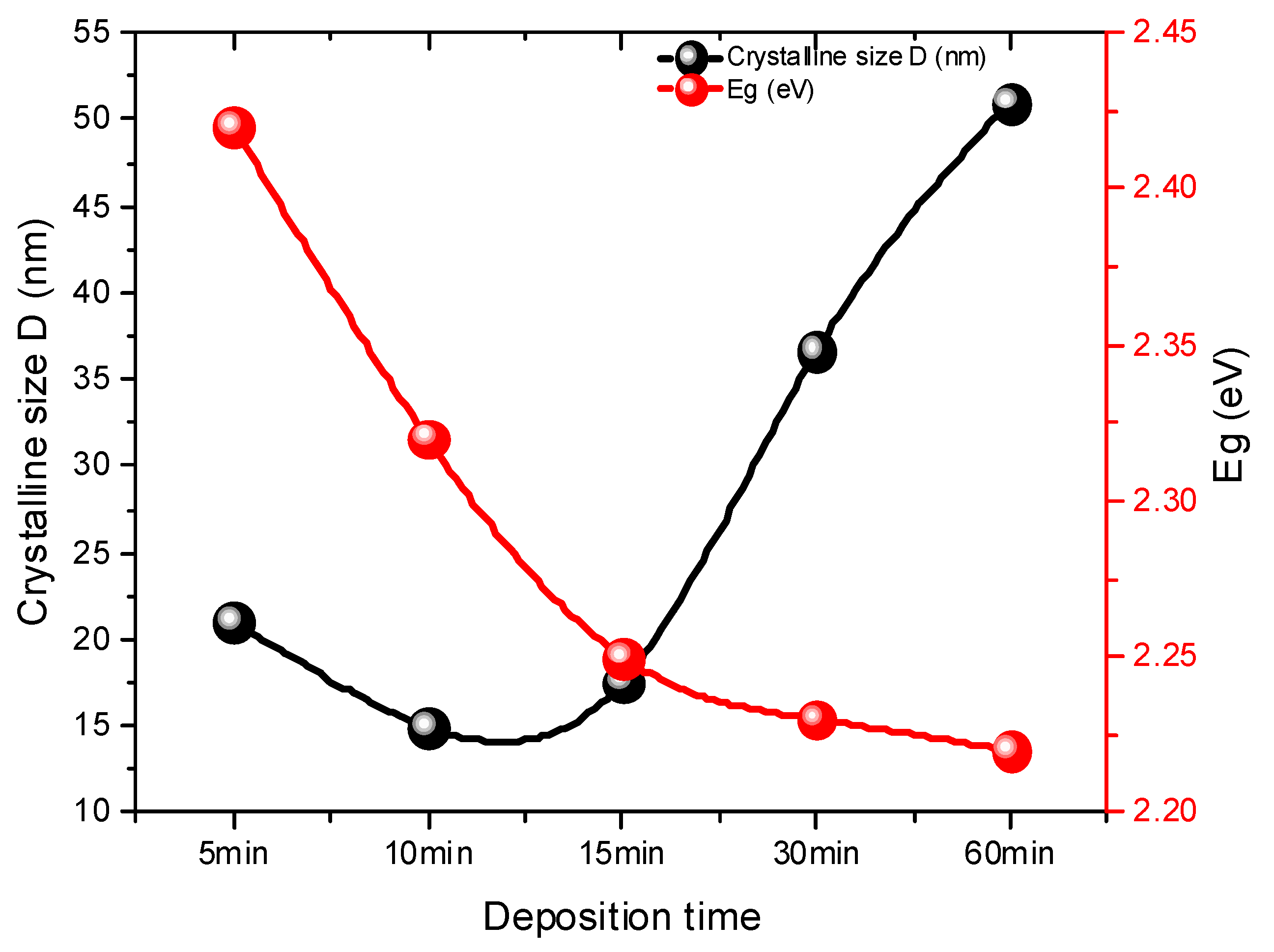
| Deposition Time (min) | FWHM | 2 θ (111) | dhkl (Å) | a (Å) | D (nm) | δ × 1014 Lines/m2 | Band Gap (eV) | |
|---|---|---|---|---|---|---|---|---|
| 5 | 0.39 | 26.37 | 3.38 | 5.85 | 21.08 | 0.002251 | 3.40 | 2.40 |
| 10 | 0.55 | 26.39 | 3.38 | 5.84 | 14.97 | 0.004465 | 4.79 | 2.32 |
| 15 | 0.47 | 26.36 | 3.34 | 5.79 | 17.50 | 0.003264 | 4.10 | 2.25 |
| 30 | 0.22 | 26.66 | 3.34 | 5.79 | 36.60 | 0.000747 | 1.93 | 2.23 |
| 60 | 0.16 | 26.38 | 3.38 | 5.85 | 50.98 | 0.000385 | 1.41 | 2.21 |
Disclaimer/Publisher’s Note: The statements, opinions and data contained in all publications are solely those of the individual author(s) and contributor(s) and not of MDPI and/or the editor(s). MDPI and/or the editor(s) disclaim responsibility for any injury to people or property resulting from any ideas, methods, instructions or products referred to in the content. |
© 2023 by the authors. Licensee MDPI, Basel, Switzerland. This article is an open access article distributed under the terms and conditions of the Creative Commons Attribution (CC BY) license (https://creativecommons.org/licenses/by/4.0/).
Share and Cite
El-Shaer, A.; Ezzat, S.; Habib, M.A.; Alduaij, O.K.; Meaz, T.M.; El-Attar, S.A. Influence of Deposition Time on Structural, Morphological, and Optical Properties of CdS Thin Films Grown by Low-Cost Chemical Bath Deposition. Crystals 2023, 13, 788. https://doi.org/10.3390/cryst13050788
El-Shaer A, Ezzat S, Habib MA, Alduaij OK, Meaz TM, El-Attar SA. Influence of Deposition Time on Structural, Morphological, and Optical Properties of CdS Thin Films Grown by Low-Cost Chemical Bath Deposition. Crystals. 2023; 13(5):788. https://doi.org/10.3390/cryst13050788
Chicago/Turabian StyleEl-Shaer, Abdelhamid, Sameh Ezzat, Mohamed A. Habib, Omar K. Alduaij, Talaat M. Meaz, and Samy A. El-Attar. 2023. "Influence of Deposition Time on Structural, Morphological, and Optical Properties of CdS Thin Films Grown by Low-Cost Chemical Bath Deposition" Crystals 13, no. 5: 788. https://doi.org/10.3390/cryst13050788