
Review of First Principles Simulations of STO/BTO, STO/PTO, and SZO/PZO (001) Heterostructures


1
Institute of Solid State Physics, University of Latvia, 8 Kengaraga Str., LV-1063 Riga, Latvia
2
Laboratory of Theoretical and Computational Chemistry, Institute of Theoretical Chemistry, Jilin University, Changchun 130023, China
*
Author to whom correspondence should be addressed.
Crystals 2023, 13(5), 799; https://doi.org/10.3390/cryst13050799
Submission received: 26 March 2023
/
Revised: 5 May 2023
/
Accepted: 8 May 2023
/
Published: 10 May 2023
(This article belongs to the Special Issue Electronic Phenomena of Transition Metal Oxides Volume II)
Abstract
:In this study, we review our first-principles simulations for STO/BTO, STO/PTO, and SZO/PZO (001) heterostructures. Specifically, we report ab initio B3PW calculations for STO/BTO, STO/PTO, and SZO/PZO (001) interfaces, considering non-stoichiometric heterostructures in the process. Our ab initio B3PW calculations demonstrate that charge redistribution in the (001) interface region only subtly affects electronic structures. However, changes in stoichiometry result in significant shifts in band edges. The computed band gaps for the STO/BTO, STO/PTO, and SZO/PZO (001) interfaces are primarily determined according to whether the topmost layer of the augmented (001) film has an AO or BO2 termination. We predict an increase in the covalency of B-O bonds near the STO/BTO, STO/PTO, and SZO/PZO (001) heterostructures as compared to the BTO, PTO, and PZO bulk materials.
1. Introduction
The new and cutting-edge technologies that have appeared over the last decade allow for the growth of STO/BTO, STO/PTO, and SZO/PZO (001) superlattices as well as ultrathin films with atomic-level control. Various aspects of the (001) surface and interface phenomena, which take place in ABO3 perovskites and their nanostructures, as well as the nature of their surfaces and interface states are very hot topics in modern theoretical solid-state physics [1,2,3,4,5,6,7,8,9,10,11,12,13,14,15,16,17,18,19,20,21,22,23,24,25,26,27]. All our ab initio calculated PbTiO3 (PTO), BaTiO3 (BTO), SrTiO3 (STO), PbZrO3 (PZO), and SrZrO3 (SZO) complex oxide materials belong to the class of so-called ABO3 perovskites. All five of our first-principles-simulated ABO3 complex oxide materials have the same primitive cubic lattice space group (group number 221). PTO complex oxide thin films have powerful spontaneous electrical polarization; accordingly, they are extensively used in numerous technologically important devices [28,29]. BTO is an important perovskite ceramic and possesses excellent dielectric, ferroelectric, and piezoelectric properties [30,31]. STO is a typical ABO3 perovskite crystal with high photocatalytic activity and excellent electronic properties. It has numerous applications in electronics, sensors, catalysts, and energy storage devices [32,33,34]. PZO perovskite has been frequently mentioned in connection with energy storage performance [35,36,37]. SZO has huge potential for a wide variety of technologically important applications, such as high-temperature oxygen sensors, capacitors, and devices capable of violet blue light emission [38,39]. Considering this great technological importance, PTO, BTO, STO, PZO, and SZO complex oxide materials as well as their (001) surfaces were exhaustively inspected worldwide during the last quarter of a century [1,2,3,4,5,6,7,8,9,10,11,12,13,14,15,16,17,18,19,20,21,22,23,24,25,26,27,40,41,42,43,44,45,46,47,48,49,50,51,52,53,54,55,56,57,58,59,60,61,62]. Nevertheless, their STO/BTO, STO/PTO, and SZO/PZO (001) interfaces are considerably less studied; therefore, additional studies and a systematic review of the existing contributions are required [63,64,65,66,67,68,69,70,71,72,73,74,75,76,77,78,79,80,81,82,83,84,85,86,87,88,89,90,91].
So far, Al-Aqtash et al. [63], at an ab initio level, studied the ferroelectric properties of BZO/PZO and SZO/PZO superlattices, which are related to our current work. Kim et al. [92] studied the remarkable non-linear dielectric properties of BTO/STO superlattices. Johnston et al. [93] performed ab initio computations of polarization and symmetry lowering in BTO/STO superlattices. Neaton and Rabe [94] developed a theory of polarization intensification in epitaxial BTO/STO superlattices. Dawber et al. [95] found the uncommon performance of ferroelectric polarization in PTO/STO superlattices. It is worth noting that in recent years, a great number of ab initio calculations were also performed for related ABO3/CDO3 interfaces. For example, Ohtomo and Hwang [96] investigated a model (001) interface amid two insulating perovskites LaAlO3 (LAO) and SrTiO3. Recently, Wang et al. [97] carried out ab initio calculations in order to examine the electronic and atomic structure of the LAO/STO (001) interface system under strain. Recently, Cancellieri et al. [98] experimentally detected a polaronic metal state at the LAO/STO (001) interface. Yan et al. [99] reported photoresponsive characteristics observed at the (001), (110), and (111) LAO/STO interfaces. Finally, Yan et al. [100] investigated the control of magnetism via doping at LAO/STO heterointerfaces.
It is well known that, in most cases, ABO3 perovskites display various formative phase transitions. They start in the cubic paraelectric phase, which is stable at high temperature, occurring as a function of the lowered temperature [101,102,103,104,105,106]. For example, PTO perovskite is stable at room temperature (RT) in the tetragonal phase [107]. Namely, it has a tetragonal phase [107] by the space group P4mm. Then, at a high temperature equal to 766 K, PTO perovskite undergoes a single phase transition [107] to a cubic, high-symmetry structure ). In contrast to PTO, BTO perovskite undergoes three phase transitions [108]. Namely, at 183 K temperature, BTO perovskite’s structure changes from a rhombohedral phase (space group R3m) to an orthorhombic phase (space group Amm2) [108]. At a temperature of 278 K, BTO perovskite’s structure changes to a tetragonal phase (P4mm) [108]. Finally, at a temperature of 403 K, BTO perovskite’s structure changes to a cubic, high-temperature structure ) [108]. Opposite to PTO and BTO perovskites, which exhibit different phase transitions, STO is a paraelectric perovskite that at all observed temperatures maintains a centrosymmetric cubic structure with a space group equal to ) [109,110]. PZO perovskite has three different phases. PZO perovskite has an orthorhombic antiferroelectric phase that is stable at temperatures up to 230 °C [111,112]. From 230 °C to 233 °C, PZO enters a rhombohedral ferroelectric phase [111,112]. PZO has a highly symmetrical cubic paraelectric phase when the temperature is above 233 °C [111,112]. Finally, there are three phase transitions in the SZO perovskite matrix [113,114]. They were detected through enthalphy measurements performed by Ligny et al. [113] and are as follows: orthorhombic phase (Pnma) ↔ orthorhombic phase (Cmcm) ↔ tetragonal phase (I4/mcm) ↔ cubic phase ) [113]. These three phase transitions in the SZO perovskite matrix occur at 995 K, 1105 K, and 1140 K, respectively [113,114].
The objective of this review paper is to conduct supplementary ab initio calculations to complete a decade-long research effort focused on the ab initio analysis of STO/BTO, STO/PTO, and SZO/PZO (001) interfaces. Our review paper is organized as follows: Section 2 outlines the calculation details. Section 3, the core of this review paper, presents an overview of atomic relaxation, electronic charge distribution, and alterations in the band structure for our ab initio computed STO/BTO, STO/PTO, and SZO/PZO (001) heterostructures. The ab initio calculation results are meticulously examined, and common systematic trends among all three STO/BTO, STO/PTO, and SZO/PZO (001) interfaces are identified and organized in a manner easily accessible to a global audience of readers. Lastly, Section 4 summarizes the conclusions of our work.
2. Computational Methods and Materials
We performed ab initio computations for STO/BTO, STO/PTO, and SZO/PZO (001) interfaces by means of the hybrid exchange-correlation functional B3PW [115,116,117] as well as the CRYSTAL computer program package [118]. It is worth noting that the B3PW exchange-correlation functional is also known as (B3PW91), i.e., Becke’s 3 parameter exchange (B3) [115] combined with the non-local correlation (PW91) [116,117]. In order to determine the performance of different exchange-correlation functionals, we computed the Γ-Γ band gap for the BaZrO3 (BZO) perovskite [29] as well as MgF2 [119] and CaF2 [120] (Table 1). The experimentally detected BZO (5.3 eV) [121], MgF2 (13.0 eV) [122], and CaF2 (12.1 eV) [123] bulk Γ-Γ band gaps are presented in Table 1 for comparative purposes. As we can see from Table 1, the Hartree–Fock (HF) [124,125] method, for BZO, MgF2, and CaF2 materials computed ab initio, very highly overestimates the experimentally detected bulk Γ-Γ band gaps. At the same time, in our density functional theory simulations (DFT), we employed local density approximation (LDA) along with the Dirac–Slater [126] exchange and the Vosko Wilk Nussair correlation [127] energy functionals in addition to the package of GGA exchange-correlation functionals proposed by Perdew-Wang (PWGGA) [117]. It is worth noting that PWGGA is the keyword in the CRYSTAL17 manual [118]. It is commonly known as PW91 [117]. Unfortunately, in contrast to the HF method, the PWGGA very strongly underestimates the bulk Γ-Γ band gap at the BZO, MgF2, and CaF2 matrixes (Table 1). Based on Table 1, it follows that the hybrid exchange-correlation functionals, such as B3LYP [128] and B3PW [115,116,117], allows us to achieve as-good-as-possible coincidence between the ab initio simulated and the experimental bulk Γ-Γ band gaps for our three simulated materials (BZO, MgF2, and CaF2) Nevertheless, the agreement between the experimental Γ-Γ bulk band gaps in the BZO, MgF2, and CaF2 matrixes and our computed Γ-Γ bulk band gap is slightly better for B3PW than for B3LYP. Due to this tiny difference in bulk band gap computations, we chose the B3PW hybrid exchange-correlation functional for all our future STO/BTO, STO/PTO, and SZO/PZO (001) interface computations. The key reason for such perfect agreement between the experiment and theory is that the hybrid B3LYP and B3PW functionals incorporate a portion of the exact exchange energy density from the HF method (20%). At the same time, the remnant of the exchange-correlation segment is the mixture of several approaches, both exchange and correlation. Therefore, we carried out all our forthcoming STO/BTO, STO/PTO, and SZO/PZO (001) heterostructure ab initio simulations using the B3PW hybrid exchange-correlation functional (Table 1).
One of the key advantages of the CRYSTAL [118] computer program, which is of crucial importance for B3PW simulations of STO/BTO, STO/PTO, and SZO/PZO (001) heterostructures, is the possibility of using the two-dimensional (2D) isolated slab model. We calculated [2] the energy convergence as a function of 2D slab thickness. Namely, we calculated the change in energy when one STO layer was added to the slab, with the ultimate goal being the acquisition of meaningful surface energies [2,129,130]. When the energy difference is less than 1 mHa, convergence is achieved. For STO perovskite [2], the slabs, which contained seven layers, meet these criteria. In the performed B3PW simulations, reciprocal space integration [131] was executed by scanning the Brillouin zone with an 8 × 8 × 8-fold-extended Pack Monkhorst [131] mesh for the ABO3 perovskite bulk and an 8 × 8 × 1-fold-expanded mesh for their (001) heterostructures. With the aim of attaining the highest possible accuracy of our B3PW simulations, we used sufficiently large tolerances, such as 7, 8, 7, 7, and 14, for the Coulomb overlap, Coulomb penetration, exchange overlap, first exchange pseudo-overlap, and second exchange pseudo-overlap, respectively [118]. We relaxed the STO/BTO, STO/PTO, and SZO/PZO (001) interface atom atomic coordinates via the (001) heterostructure’s total energy minimization. Regarding the (001) interface’s atomic coordinate relaxation, we used our developed computer code. This code combines the conjugated gradient optimization technique [132] with numerical calculation of derivatives [132]. To describe the chemical bonding in the STO/BTO, STO/PTO, and SZO/PZO (001) heterostructures as well as covalency effects, we used Mulliken [133,134] population analysis. For our ab initio computed Pb, Sr, Ba, Ti, and O (001) interface atoms, we employed the basis sets described in [135]. The inner core electrons for Zr, Sr, Pb, Ba, and Ti atoms were described using the small core Hay Wadt effective pseudopotentials [118,136]. We described the oxygen atoms using the all-electron basis set [118,135].
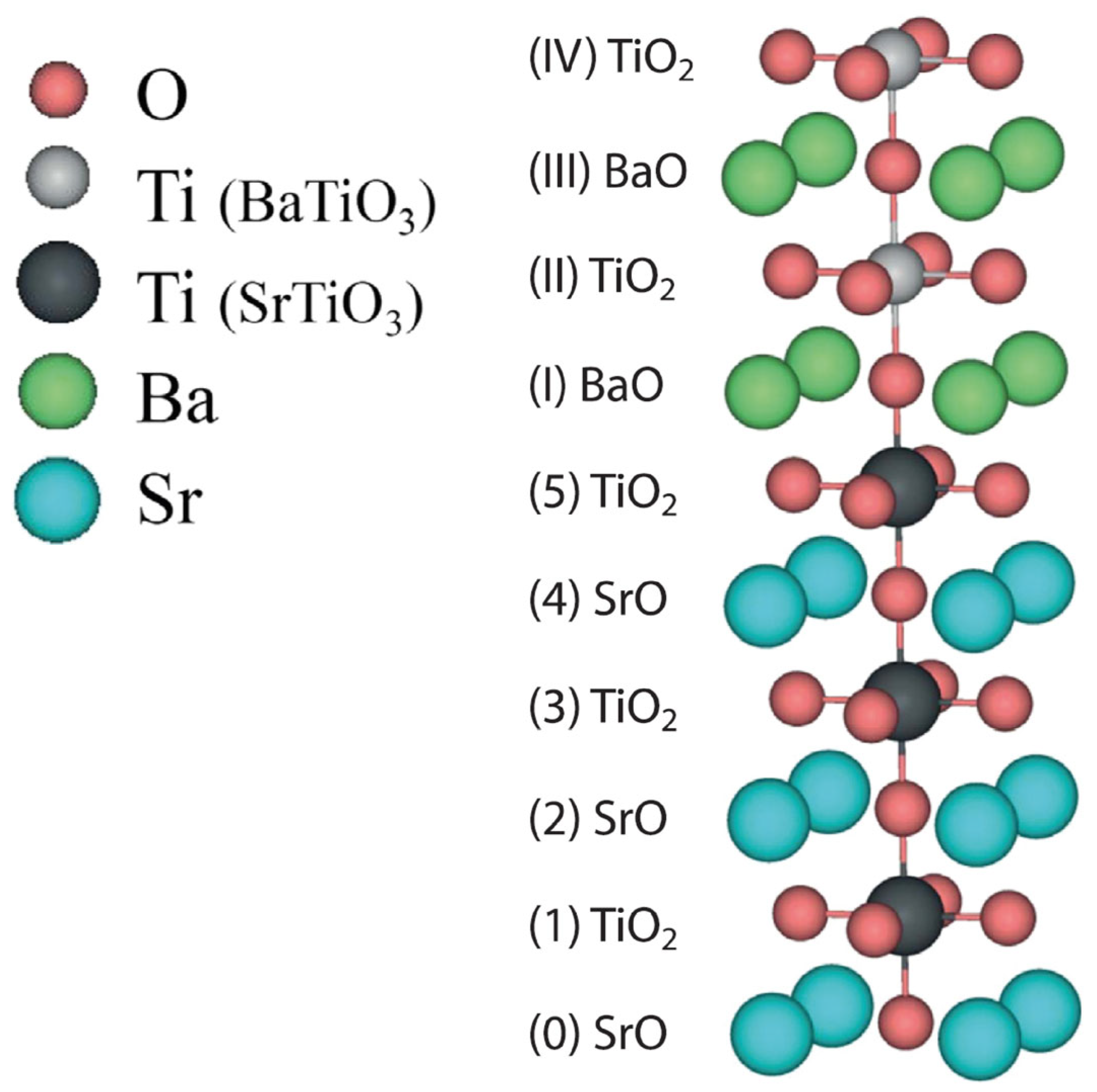
At this stage, we will explain our ab initio computation details for the BTO/STO (001) interface, which will account for the fact that we also used the same model for STO/PTO and SZO/PZO (001) heterostructures. The STO substrate, at room temperature, has a cubic, high-symmetry structure that corresponds to the space group ). In order to save computational time and focus on the key physics, in our ab initio simulations, we modelled the STO and BTO perovskites at their cubic, high-symmetry phase. We computed the STO/BTO, STO/PTO, and SZO/PZO (001) heterostructures using the single (001)-slab model. In our first-principles simulations, a TiO2-terminated STO (001) substrate was formed from 11 alternating SrO and TiO2 layers (Figure 1) with an SrO layer located in the middle of the substrate. On both sides of the TiO2-terminated 11-layer STO (001) substrate (Figure 1), we augmented from 1 to 10 BaO and TiO2-terminated alternating BTO perovskite (001) layers.
In the performed ab initio B3PW simulations, we allowed all atoms of the STO/BTO, STO/PTO, and SZO/PZO (001) heterostructures to relax. Atomic relaxations are a result of the cubic symmetry restrictions enforced on the system, which only occur along the z axis (Figure 1). The lattice mismatch of approximately 2.5% between the BTO perovskite and STO bulk (Figure 1) lattice constants occurs during BTO’s epitaxial growth. Our ab initio B3PW-computed joint average equilibrium lattice constant, which is used in our forthcoming simulations of STO/BTO (001) heterostructures (Figure 1), is equal to 3.958 Å. We computed the joint lattice constant (3.958 Å) for the STO/BTO (001) heterostructure in the case of the thickest possible (001) interface, consisting of the 11-layer STO (001) substrate, and on both sides (Figure 1) of this substrate’s symmetrically augmented 10 BaTiO3 (001) layers. In order to simulate the shift (Δz) of each layer for the STO/BTO (001) interface, we accounted for the displacement magnitude of the previous (Figure 1) atomic layer. Thus, the reference coordinate z for each monolayer N was calculated using the subsequent expression:
where zN-1Me and zN-1O describe the z coordinates for a cation and an anion located in the previous atomic monolayer.
zNref = ½ [zN-1Me + zN-1O),
3. Ab Initio Calculation Results
3.1. Ab Initio B3PW-Computed ABO3 Perovskite Bulk Properties
As the starting point of our ab initio simulations, we computed the bulk lattice constants of BTO, PTO, STO, SZO, and PZO (Table 2). It is worth noting that our ab initio B3PW-computed BTO (4.008 Å), PTO (3.936 Å), STO (3.904 Å), SZO (4.195 Å), and PZO (4.220 Å) bulk lattice constants (Table 2) are in fair agreement with the available experimentally measured bulk lattice constants [137,138,139,140,141]. The experimentally measured BTO, PTO, STO, SZO, and PZO bulk lattice constants are equal to 4.004 Å [137], 3.97 Å [138], 3.898 Å [139], 4.154 Å [140], and 4.1614 Å [141], respectively (Table 2).
As evident in Figure 2 and Table 3, our first-principles B3PW-simulated PTO perovskite bulk Γ-Γ band gap is equal to 4.32 eV [142]. The experimentally detected PTO perovskite bulk Γ-Γ band gap in the tetragonal phase is equal to 3.4 eV [121], which coincides fairly well with our ab initio B3PW simulation result of 4.32 eV [142] (Figure 2a and Table 3). The BTO perovskite Γ-Γ bulk band gap was experimentally detected at a temperature of 278 K [143], which coincides with the BTO tetragonal-to-orthorhombic phase transition. It is equal to 3.27 or 3.38 eV under different experimental conditions [143] (Table 3). Our first-principles B3PW-simulated BTO bulk Γ-Γ band gap is (3.55 eV) [142] (Table 3 and Figure 2b), which in outstanding agreement with the abovementioned experimental data [143]. Finally, our first-principles B3PW-simulated STO bulk Γ-Γ band gap (3.96 eV) is in excellent agreement with the experimentally available results for the STO bulk band gap at a Γ-point equal to 3.75 eV [144].
Our ab initio B3PW-simulated effective atomic charges and bond population values for the BTO, PTO, STO, SZO, and PZO perovskites are collected in Table 4. As we can see from Table 4, our ab initio B3PW-computed atomic charges for all five computed perovskites are considerably smaller than their perfect ionic values equal to +2e, +4e, and −2e for A, B, and O atoms, respectively (Table 4). According to our ab initio B3PW computations, the largest chemical bond populations are between the Ti and O atoms (0.100e) in the BTO perovskite and between the Zr and O atoms (0.100e) in the PZO perovskite (Table 4).
3.2. Ab Initio B3PW-Computed STO/BTO (001) Interfaces
We carried out ab initio B3PW computations of the STO/BTO (001) heterostructures [77,91] by means of the symmetrically terminated slab model (Figure 1). The TiO2-terminated STO (001) substrate contained eleven atomic monolayers (Figure 1). As a next step, we simulated monolayer-by-monolayer epitaxial growth (Figure 1 and Table 5); namely, we added a pair of respective BTO (001) monolayers on both sides of the symmetrical 11-layer STO (001) substrate (Figure 1).
We added from one BTO (001) monolayer (Figure 1 and Table 5) up to ten BTO monolayers on both sides of the eleven-layer TiO2-terminated STO (001) substrate. Thus, we designed ten STO/BTO (001) interfaces, which contained different thicknesses (from one to ten monolayers) of deposited BTO (001) nano-film (Figure 1 and Table 5). Considering the symmetry restrictions, in our ab initio computations, all atom atomic positions (Figure 1) were relaxed only along the z axis (Table 5). Atomic displacements (Δz) were computed regarding the averaged position (z) of the preceding atomic monolayer (Figure 1), as described in Equation (1). Our obtained ab initio calculation results are collected in Table 5. As we can see from Table 5, all our first-principles-computed displacements are less than 5% of a0, i.e., the TiO2-terminated STO (001) substrates become larger on average with respect to the bulk phase (Table 5). At the same time and in stark contrast, the BTO (001) thin film contracts in order to recompensate the lattice mismatch (Table 5).
As it is possible to see from Figure 3 and Table 5, our ab initio simulated TiO2-terminated STO (001) substrate’s upper layer (x = 0 in Figure 3), which contains Ti and O atoms, very strongly shifts towards the perovskite bulk (−5.95% of a0). According to our ab initio simulations (Table 5), upper-BTO (001)-layer atoms, which accumulate on the TiO2-terminated eleven-layer STO (001) substrate, rather actively relax (Δz) inwards every time (x = 1–10 in Figure 3). It is very important to stress that the BTO’s augmented upper (001)-layer atoms’ inward shift numerical value Δz (Table 5) very actively depend on the number of augmented BTO (001) layers (odd or even), which describe upper augmented layer termination (BaO or TiO2) (Figure 3 and Table 5). For example, for one augmented BTO (001) layer, which consists of Ba and O atoms, the atom shift size Δz is equal to (−1.54%) of a0 (Table 5 and Figure 3). For the case of two augmented BTO (001) layers, where the top BTO (001) layer consists of Ti and O atoms, the respective top layer atom shift size Δz is equal to (−3.20% of a0) (Figure 3 and Table 5). For three augmented BTO (001) layers, the top-layer Ba and O atom shift size Δz is (−1.84% of a0) (Table 5 and Figure 3).
Table 5 presents the total Mulliken charges of the atomic planes of SrO, TiO2, and BaO (001) and the Mulliken charges of all atoms inside these planes, namely, QSr, QTi, QO and QBa, according to our computations for STO/BTO (001) heterostructures (Table 5). Since the Ti-O bond is partly covalent, according to our ab initio computations for STO/BTO (001) heterostructures, the Mulliken net charges for Ti and O atoms are different from their well-known ionic values of (+4e) and (−2e). Our ab initio computed Mulliken charges for atoms in the STO and BTO bulk matrixes are collected in Table 4. As we have demonstrated in our recent ab initio computations [6], the Ti-O bond population around the TiO2-terminated BTO (0.126e) and STO (0.118e) (001) surfaces increases its covalency regarding the Ti-O bond population in the BTO (0.100e) and STO (0.088e) bulk matrixes. Notably, an increase in the Ti-O bond covalency, in comparison to the BTO bulk (0.126e vs. 0.100e), is observed around our ab initio computed STO/BTO (001) heterostructure. It is important to stress once more that related effects, including an increase in the chemical bond populations near the (001) and especially (011) surfaces with respect to the bulk value, were observed for all our ab initio calculated ABO3 perovskites [2,3,4,5,6,14,19]. According to our ab initio computations collected in Table 5, the (001) surface planes of the TiO2-terminated BTO (001) films deposited on the eleven-layer STO (001) substrate attract ~0.25e. At the same time, the BaO-terminated STO/BTO (001) heterostructures (Figure 1) become more positively charged in order to compensate for surface relaxation (Table 5). Thus, the (001) surface Ba-O chemical bond covalency is only very modestly increased. At the same time, our ab initio computed covalency of the (001) surface Ti-O chemical bond is considerably larger than in the bulk. This may compensate for the relatively small (001) surface relaxation magnitude of the BaO-terminated STO/BTO (001) heterostructures (Figure 1) regarding the TiO2-terminated respective (001) interfaces (Table 5 and Figure 3). In both TiO2-terminated stoichiometric and BaO-terminated non-stoichiometric STO/BTO (001) interfaces, charges on the substrate monolayer (Table 5) did not change substantially. Namely, for stoichiometric and non-stoichiometric (001) STO/BTO heterostructures, these are equal to ±0.03e for the TiO2-terminated and BaO-terminated interfaces (Table 5). The strongest aberrations in the atomic charges for the STO/BTO (001) interfaces are in the topmost monolayer ~± 0.26e for the stoichiometric structures and at −0.23e in the non-stoichiometric structures (Table 5).
Difference electron charge density maps provide a further chance to visualize the electronic charge density reallocation in the STO/BTO (001) heterostructures (Figure 4) in comparison to the lonely STO and BTO (001) slab components. Charge density reallocation is described as the electronic density in the (001) interface minus the sum of electron densities in the sequentially isolated STO (001) substrate and BTO (001) thin film slabs (Figure 4) for both 3 and 4 UC thick STO/BTO (001) heterostructures. These difference electron charge density maps (Figure 2) display that the most significant distortions occur at the (001) interface and are caused by the re-compensation of the (001) surface effects of the (001) slabs.
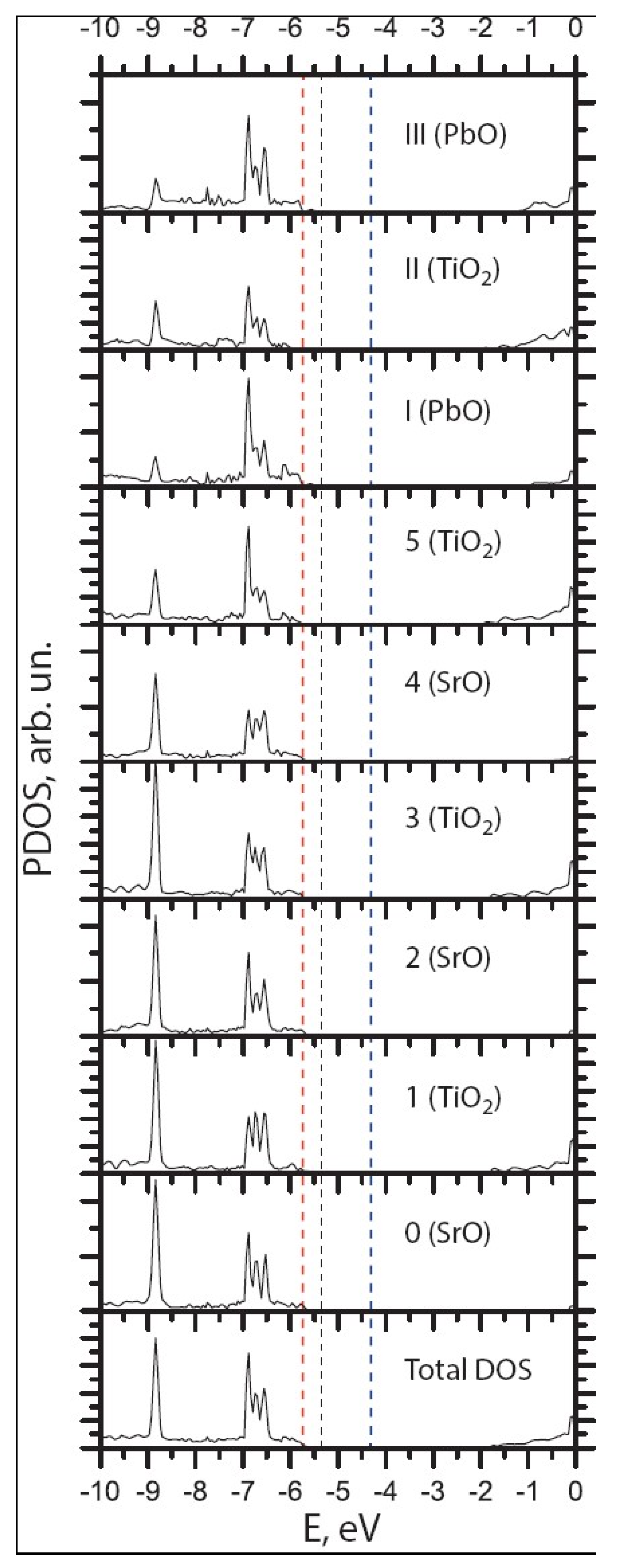
Figure 5 and Figure 6 depict our ab initio B3PW-computed, DOS-expressed, layer-by-layer results for all orbitals of the Sr, Ba, O, and Ti atoms of the 3 and 4 UC thick STO/BTO (001) heterostructures (Figure 5 and Figure 6). Akin to the bulk ABO3 perovskites, the valence band at the top (VB) consists of O 2p orbitals, but the bottom of the conduction band (CB) mostly consists of Ti 3d states (Figure 5 and Figure 6). The hybridization among the Ti and O atoms is also very well pronounced (Figure 5 and Figure 6).
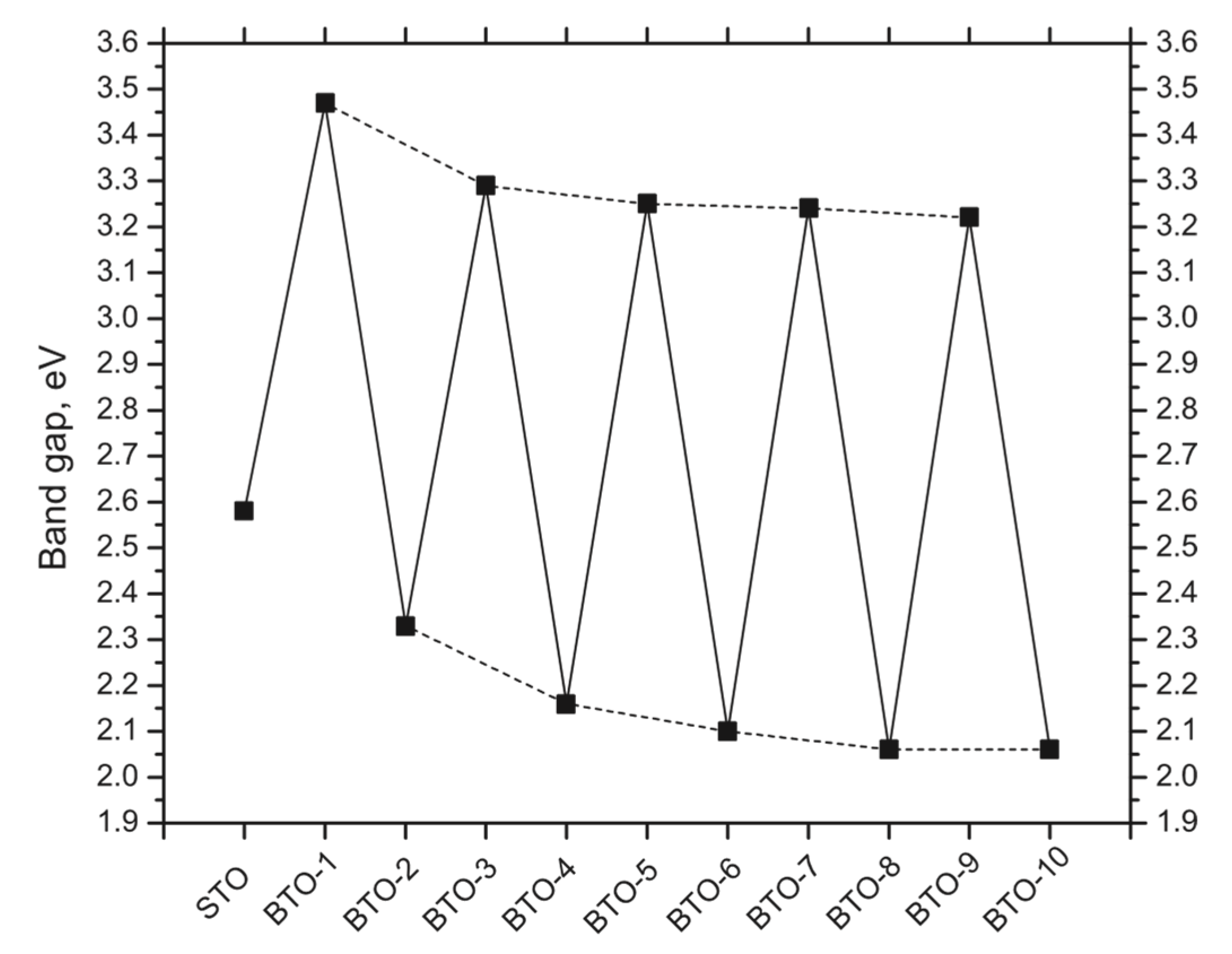
Our ab initio B3PW-computed STO bulk direct band gap (3.96 eV) (Table 3) coincides very well with the respective experimental value of 3.75 eV [144]. In addition, our ab initio B3PW-computed BTO direct bulk band gap equal to 3.55 eV (Table 4) is in fair agreement with the available experimental data measured at a temperature of 278 K (3.27 eV and 3.38 eV) [143] (Table 4). For the BaO-terminated STO/BTO (001) heterostructure (Figure 5), the obtained surplus of electron density increases the occupied levels, thereby giving rise to the expanded band gap (Table 5). In contrast, the TiO2-terminated STO/BTO (001) heterostructure (Figure 6) experiences an absence of electron density that decreases the occupied levels, thereby lowering the band gap of the stoichiometric STO/BTO (001) heterostructures (Figure 7).
3.3. Ab Initio B3PW-Computed STO/PTO (001) Interfaces
For the STO/PTO (001) interface substrate, we employed a symmetrical STO (001) slab (Figure 8) containing 11 alternating SrO and TiO2 layers (TiO2_SrO_TiO2_SrO_TiO2_SrO_TiO2_SrO_TiO2_SrO_TiO2). So, in our first-principles simulations, the STO (001) substrate consisted of a supercell that contained 28 atoms (Figure 8). Thus, in our first-principles simulations, the STO (001) substrate is non-stoichiometric and consists of Sr5Ti6O17 formula units per cell (Figure 8).
Next, we gradually and symmetrically augmented from one to ten alternating PbO and TiO2 layers (PbO_TiO2_PbO_TiO2_PbO_TiO2_PbO_TiO2_PbO_TiO2) on both sides of the SrTiO3 (001) substrate. So, the STO/PTO (001) interface in our ab initio computations contained an eleven-layer STO (001) substrate, which consisted of 28 atoms, and 10 PTO (001) layers, which consisted of 25 atoms that were symmetrically augmented on both sides on the (001) substrate (Figure 8). Thus, the largest atom number in the ab initio STO/PTO (001) interface computations was 78 atoms, with a unit cell formula equal to Sr5Pb10Ti16O47. It is worth noting that during the epitaxial PTO (001) film growth (Figure 8), lattice mismatch between the PTO and STO bulk lattice constants arose (Table 2). Therefore, in the first-principles B3PW simulations, we optimized the joint STO/PTO (001) interface lattice constant for the thickest computed STO/PTO (001) interface, which consisted of 31 layers and 78 atoms, in order to minimize the strain effect [72,87]. Our ab initio B3PW-computed STO/PTO (001) interface joint lattice constant is equal to 3.91 Å.
In our first-principles B3PW simulations, the atomic displacements Δz along the z axis were computed in association with the averaged z position of the previous layer, as reported in Equation (1). As evident in Figure 9, for one augmented PTO (001) layer (x = 1), consisting of PbO atoms, on top of the eleven-layer STO (001) substrate, the top layer PbO atom shift size Δz is equal to −6.01% of a0 (Figure 9). It is worth noting that in Figure 9, (x = 0) corresponds to the shift magnitude (Δz) of the STO (001) substrate’s top-layer TiO2 atoms (Figure 9). For two augmented PTO (001) layers, the upper layer contains TiO2 atoms (x = 2) whose shift size (Δz) is (−7.76% of a0) (Figure 9). For three augmented PTO (001) layers (x = 3), the top layer again contains PbO atoms, and their shift size Δz is (−6.97% of a0) (Figure 9).
Due to the significant covalency effects in the Ti-O chemical bonds of PTO perovskite (Table 4), our ab initio B3PW-computed Mulliken charges for Ti (+2.34e) and O(−1.23e) atoms are rather different from the formal ionic charges of Ti and O (equal to +4e and −2e, respectively). As a result of the performed ab initio B3PW computations, an increase in Ti-O chemical bond covalency (0.158e) with respect to the PTO bulk (0.098e) was noted near the STO/PTO (001) interface. The augmented PTO (001) film’s upper-layer TiO2 planes, separately from their numbers of augmented layers, which are equal to two, four, six, eight, or ten, in all cases attracts only 0.08e. In contrast, the PbO-terminated STO/PTO (001) interfaces become more positive, namely, +0.13e for one augmented PTO layer, +0.14e for three layers, +0.14e (five layers), +0.15e (seven layers), and 0.15e (nine layers).
Figure 10 describes the electronic charge density redistribution at the STO/PTO (001) interfaces with respect to the pure STO and PTO (001) slabs (Figure 10). As is known, charge density reallocation is defined as the electron density (001) on the heterostructure minus the sum of electron densities in the separately isolated STO (001) substrate and PTO (001) film slabs, as illustrated in Figure 10 for both 3- and 4 UC thick STO/PTO (001) heterostructures. Figure 10 shows that the most important distortions take place at the (001) heterostructures and are created by the compensation for the surface effects of the slabs. The difference electron charge density maps (Figure 10) also show that the electronic structure of the STO (001) substrate of the non-stoichiometric STO/PTO (001) interfaces is distorted to a degree equal to that of the stoichiometric interfaces (Figure 10).
Our ab initio B3PW-computed DOS values, which were considered layer-by-layer on all orbitals of Sr, Pb, O, and Ti atoms of the three- and four-unit-cell (UC)-thick STO/PTO (001) interfaces, are depicted in Figure 11 and Figure 12. As with all bulk ABO3 perovskites, the top of the valence band for the STO/PTO (001) interface consists mainly of O2p orbitals, whereas the bottom of the CB for the STO/PTO (001) interfaces is mostly composed of Ti3d atomic orbitals.
The first-principles B3PW-simulated band gap for the PbO-terminated PTO (001) film augmented on the STO (001) substrate, which contains one layer (x = 1), is 3.45 eV (Figure 13 and Figure 14). The PbO-terminated augmented PTO (001) film band gaps for systems that contain three, five, seven, and nine layers are 3.25 eV, 3.08 eV, 2.99 eV, and 2.94 eV (Figure 13 and Figure 14). The first-principles-simulated band gaps for the TiO2-terminated PTO (001) film, augmented on the STO (001) substrate (Figure 13 and Figure 14), which contains two, four, six, eight, and ten layers, are 3.18 eV, 3.17 eV, 3.05 eV, 2.99 eV, and 2.93 eV.
3.4. Ab Initio B3PW-Computed SZO/PZO (001) Interfaces
Additionally, our ab initio computations for the SZO/PZO (001) heterostructures, akin to those performed for the STO/BTO and STO/PTO (001) heterostructures, were carried out using the symmetrically terminated slab model [72,77,83]. The SrZrO3 (001) substrate consisted of 11 monolayers, and it was terminated with ZrO2 monolayers on both sides. Then, monolayer-by-monolayer epitaxial growth was modelled. Namely, we symmetrically added a pair of PZO (001) monolayers symmetrically to both sides of a SZO (001) eleven-layer substrate slab until the deposited PZO (001) film reached the thickness of ten monolayers on both sides. Thus, we constructed 10 (001) interfaces consisting of deposited PZO (001) nano-films with different thicknesses.
As a next step, in order to determine the level of electronic charge density reallocation, we analyzed the behavior of the electronic charge density on the (001) interfaces. We compared our results to the isolated BTO, PbZO, and STO and SZO (001) slabs (Figure 15). The difference electron charge density plots (Figure 15) demonstrate that the major distortions occur at the (001) heterostructure. They occur due to the compensation for the first-principles-computed surface effects of the slabs (Figure 15). They demonstrate that the electronic structure of the (001) substrate of the non-stoichiometric (001) interface is equally as gnarled as the stoichiometric ones. The situation for the (001) thin films is the exact opposite (Figure 15). This finding corresponds well with our forecasted atomic structures.
We carefully analyzed the DOS projected layer by layer onto all orbitals of the Sr, Ba, Pb, Ti, O, and Zr atoms of the STO/BTO and SZO/PZO (001) heterostructures. As in the case of the bulk ABO3 perovskites, the top of the VB was formed from O 2p orbitals. In contrast, the bottom of the CB was mainly formed from Ti 3d and Zr 4d states. In addition, Ti-O and Zr-O hybridization are clearly pronounced. In the case of the BaO-terminated STO/BTO (001) and ZrO2-terminated SZO/PZO (001) heterostructures, an excess of electron density shifts was gained as the number of occupied levels increased, giving rise to the expanded band gap (Figure 16). In stark contrast, the PbO and TiO2-terminated (001) heterostructures experienced a lack of electron density. This shifted the number of occupied levels down and thereby reduced the band gaps of the SZO/PZO and STO/BTO (001) interfaces (Figure 16).
4. Conclusions
In this study, we reviewed our first-principles simulations for SrTiO3/BaTiO3, SrTiO3/PbTiO3, and SrZrO3/PbZrO3 (001) interfaces. Namely, we presented ab initio B3PW computations of SrTiO3/BaTiO3, SrTiO3/PbTiO3, and SrZrO3/PbZrO3 (001) interfaces, for which non-stoichiometric heterostructures were taken into account. In our ab initio B3PW computations, we demonstrated that charge redistribution at the (001) interface region weakly affects electronic structure, while the change in stoichiometry induces significant shifts in band edges. The optical band gaps of the SrTiO3/BaTiO3, SrTiO3/PbTiO3, and SrZrO3/PbZrO3 (001) interfaces depend mostly on the AO- or BO2-termination of the upper layer of augmented (001) film. We predicted an enhancement of the B-O chemical bond covalency near the SrTiO3/BaTiO3, SrTiO3/PbTiO3, and SrZrO3/PbZrO3 (001) interfaces as compared to the BaTiO3, PbTiO3, and PbZrO3 bulk. We found that the surface covalency effects in non-stoichiometric (001) films are less pronounced than those in stoichiometric ones.
Author Contributions
Conceptualization, R.J. and D.B.; methodology, R.I.E.; software, S.P.; validation, R.I.E., R.J. and D.B.; formal analysis, R.J.; investigation, R.I.E. and R.J.; resources, D.B.; data curation, S.P.; writing—original draft preparation, R.I.E., D.B., S.P. and R.J.; writing—review and editing, R.I.E., R.J., S.P. and D.B.; visualization, S.P.; funding acquisition, D.B. All authors have read and agreed to the published version of the manuscript.
Funding
We acknowledge the financial support from our funder the Latvian Council of Science. The funding number is Grant No. LZP-2020/1-0345. The Institute of Solid-State Physics, University of Latvia (Latvia), as a center of excellence, has received funding from the European Union’s Horizon 2020 Framework Programme H2020-WIDESPREAD01-2016-2017-Teaming Phase 2 under Grant Agreement No. 739508, project CAMART-2.
Data Availability Statement
Not applicable.
Conflicts of Interest
The authors declare no conflict of interest.
References
- Dawber, M.; Rabe, K.M.; Scott, J.F. Physics of thin-film ferroelectric oxides. Rev. Mod. Phys. 2005, 77, 1083–1130. [Google Scholar] [CrossRef]
- Eglitis, R.I.; Vanderbilt, D. First-principles calculations of atomic and electronic structure of SrTiO3 (001) and (011) surfaces. Phys. Rev. B 2008, 77, 195408. [Google Scholar] [CrossRef]
- Eglitis, R.I.; Vanderbilt, D. Ab initio calculations of BaTiO3 and PbTiO3 (001) and (011) surface structures. Phys. Rev. B 2007, 76, 155439. [Google Scholar] [CrossRef]
- Eglitis, R.I.; Purans, J.; Gabrusenoks, J.; Popov, A.I.; Jia, R. Comparative ab initio calculations of ReO3, SrZrO3, BaZrO3, PbZrO3 and CaZrO3 (001) surfaces. Crystals 2020, 10, 745. [Google Scholar] [CrossRef]
- Eglitis, R.I.; Purans, J.; Jia, R. Comparative Hybrid Hartree-Fock-DFT Calculations of WO2-Terminated Cubic WO3 as well as SrTiO3, BaTiO3, PbTiO3 and CaTiO3 (001) surfaces. Crystals 2021, 11, 455. [Google Scholar] [CrossRef]
- Eglitis, R.I.; Purans, J.; Popov, A.I.; Bocharov, D.; Chekhovska, A.; Jia, R. Ab initio computations of O and AO as well as ReO2, WO2 and BO2-terminated ReO3, WO3, BaTiO3, SrTiO3 and BaZrO3 (001) surfaces. Symmetry 2022, 14, 1050. [Google Scholar] [CrossRef]
- Zhang, R.; Hwang, G.S. First-principles mechanistic study of the initial growth of SrO by atomic layer deposition on TiO2-terminated SrTiO3 (001). J. Phys. Chem. C 2020, 124, 28116. [Google Scholar] [CrossRef]
- Sambrano, J.R.; Longo, V.M.; Longo, E.; Taft, C.A. Electronic and structural properties of the (001) SrZrO3 surface. J. Mol. Struct. THEOCHEM 2007, 813, 49–56. [Google Scholar] [CrossRef]
- Brik, M.G.; Ma, C.G.; Krasnenko, V. First-principles calculations of the structural and electronic properties of the cubic CaZrO3 (001) surfaces. Surf. Sci. 2013, 608, 146–153. [Google Scholar] [CrossRef]
- Eglitis, R.I.; Kleperis, J.; Purans, J.; Popov, A.I.; Jia, R. Ab initio calculations of CaZrO3 (011) surfaces: Systematic trends in polar (011) surface calculations of ABO3 perovskites. J. Mater. Sci. 2020, 55, 203–217. [Google Scholar] [CrossRef]
- Li, W.; Landis, C.M.; Demkov, A. Domain morphology and electro-optic effect in Si-integrated epitaxial BaTiO3 films. Phys. Rev. Materials 2022, 6, 095203. [Google Scholar] [CrossRef]
- Erdman, N.; Poeppelmeier, K.R.; Asta, M.; Warschkov, O.; Ellis, D.E.; Marks, L.D. The structure and chemistry of the TiO2-rich surface of SrTiO3 (001). Nature 2002, 419, 55–58. [Google Scholar] [CrossRef]
- Celik, F.A. Electronic structure of two-dimensional-layered PbTiO3 perovskite crystal: An extended tight-binding study based on DFT. Bull. Mater. Sci. 2022, 45, 108. [Google Scholar] [CrossRef]
- Eglitis, R.I. Comparative first-principles calculations of SrTiO3, BaTiO3, PbTiO3 and CaTiO3 (001), (011) and (111) surfaces. Ferroelectrics 2015, 483, 53–67. [Google Scholar] [CrossRef]
- Zhong, M.; Zeng, W.; Liu, F.S.; Tang, B.; Liu, Q.J. First-principles study of the atomic structures, electronic properties, and surface stability of BaTiO3 (001) and (011) surfaces. Surf. Interf. Anal. 2019, 51, 1021–1032. [Google Scholar] [CrossRef]
- Costa-Amaral, R.; Gohda, Y. First-principles study of the adsorption of 3d transition metals on BaO- and TiO2-terminated cubic-phase BaTiO3 (001) surfaces. J. Chem. Phys. 2020, 152, 204701. [Google Scholar] [CrossRef] [PubMed]
- Eglitis, R.I.; Piskunov, S. First principles calculations of SrZrO3 bulk and ZrO2-terminated (001) surface F centers. Comput. Condens. Matter 2016, 7, 1–6. [Google Scholar] [CrossRef]
- Saghayezhian, M.; Sani, S.M.R.; Zhang, J.; Plummer, E.W. Rumpling and enhanced covalency at the SrTiO3 (001) surface. J. Phys. Chem. C 2019, 123, 8086–8091. [Google Scholar] [CrossRef]
- Kruchinin, S.P.; Eglitis, R.I.; Babak, V.P.; Vyshyvana, I.G.; Repetsky, S.P. Effects of Electron Correlation Inside Disordered Crystals. Crystals 2022, 12, 237. [Google Scholar] [CrossRef]
- Chun, H.J.; Lee, Y.; Kim, S.; Yoon, Y.; Kim, Y.; Park, S.C. Surface termination of BaTiO3 (111) single crystal: A combined DFT and XPS study. Appl. Surf. Sci. 2022, 578, 152018. [Google Scholar] [CrossRef]
- Alam, N.N.; Malik, N.A.; Samat, M.H.; Hussin, N.H.; Jaafar, N.K.; Radzwan, A.; Mohyedin, M.Z.; Haq, B.U.; Ali, A.M.M.; Hassan, O.H.; et al. Underlaying mechanism of surface (001) cubic ATiO3 (A = Pb,Sn) in enhancing thermoelectric performance of thin-film applications using density functional theory. Surf. Interfaces 2021, 27, 101524. [Google Scholar] [CrossRef]
- Zhao, X.; Selloni, A. Structure and stability of NaTaO3 (001) and KTaO3 (001) surfaces. Phys. Rev. Mater. 2019, 3, 015801. [Google Scholar] [CrossRef]
- Kolpak, A.M.; Li, D.; Shao, R.; Rappe, A.M.; Bonnell, D.A. Evolution of the surface structure and thermodynamic stability of the BaTiO3 (001) surface. Phys. Rev. Lett. 2008, 101, 036102. [Google Scholar] [CrossRef] [PubMed]
- Eglitis, R.; Popov, A.I.; Purans, J.; Jia., R. First principles hybrid Hartree-Fock-DFT calculations of bulk and surface F centers in oxide perovskites and alkali-earth fluorides. Low Temp. Phys. 2020, 46, 1206–1212. [Google Scholar] [CrossRef]
- Gao, H.; Yue, Z.; Liu, Y.; Hu, J.; Li, X. A first-principles study on the multiferroic property of two-dimensional BaTiO3 (001) ultrathin film with surface Ba vacancy. Nanomaterials 2019, 9, 269. [Google Scholar] [CrossRef] [PubMed]
- Iles, N.; Finocchi, F.; Khodja, K.D. A systematic study of ideal and double layer reconstruction of ABO3 (001) surfaces (A=Sr, Ba: B=Ti, Zr) from first principles. J. Phys. Condens. Matter 2010, 22, 305001. [Google Scholar] [CrossRef]
- Borstel, G.; Eglitis, R.I.; Kotomin, E.A.; Heifets, E. Modelling of defects and surfaces in perovskite ferroelectrics. Phys. Status Solidi B 2003, 236, 253–264. [Google Scholar] [CrossRef]
- Wang, Y.; Zhao, H.; Zhang, L.; Chen, J.; Xing, X. PbTiO3-based perovskite ferroelectric and multiferroic thin films. Phys. Chem. Chem. Phys. 2017, 19, 17493–17515. [Google Scholar] [CrossRef]
- Eglitis, R.I.; Popov, A.I. Systematic trends in (001) surface ab initio calculations of ABO3 perovskites. J. Saudi Chem. Soc. 2018, 22, 459–468. [Google Scholar] [CrossRef]
- Prasatkhetragarn, A.; Sareein, T.; Triamnak, N.; Yimnirun, R. Dielectric and ferroelectric properties of modified-BaTiO3 lead-free ceramics prepared by solid solution method. Ferroelectrics 2022, 586, 224–241. [Google Scholar] [CrossRef]
- Eglitis, R.I. Ab initio calculations of SrTiO3, BaTiO3, PbTiO3, CaTiO3, SrZrO3, PbZrO3 and BaZrO3 (001), (011) and (111) surfaces as well as F centers, polarons, KTN solid solutions and Nb impurities therein. Int. J. Mod. Phys. B 2014, 28, 1430009. [Google Scholar] [CrossRef]
- Zhang, M.; Lopato, E.M.; Ene, N.N.; Funni, S.D.; Du, T.; Jiang, K.; Bernard, S.; Salvador, P.A.; Rohrer, G.S. Synthesis and Structure of Ion-Exchange SrTiO3 Photocatalyst with Improved Reactivity for Hydrogen Evolution. Adv. Mater. Interfaces 2023, 10, 2202476. [Google Scholar] [CrossRef]
- Takata, T.; Jiang, J.; Sakata, Y.; Nakabayashi, M.; Shibata, N.; Nandal, V.; Seki, K.; Hisatomi, T.; Domen, K. Photocatalytic water splitting with a quantum efficiency of almost unity. Nature 2020, 581, 411–414. [Google Scholar] [CrossRef] [PubMed]
- Tailor, N.K.; Abdi-Jalebi, M.; Gupta, V.; Hu, H.; Dar, M.I.; Li, G.; Satapathi, S. Recent progress in morphology optimization in perovskite solar cells. J. Mater. Chem. A 2020, 8, 21356–21386. [Google Scholar] [CrossRef]
- Liu, X.; Zhu, G.; Li, Y.; Yang, T.; Hao, X.; Gong, W. High-performance PbZrO3-based antiferroelectric multilayer capacitors based on multiple enhancement strategy. Chem. Eng. J. 2022, 446, 136729. [Google Scholar] [CrossRef]
- Xu, R.; Zhu, Q.; Xu, Z.; Feng, Y.; Wei, X. PLZT antiferroelectric ceramics with promising energy storage and discharge performance for high power applications. J. Am. Ceram. Soc. 2020, 103, 1831–1838. [Google Scholar] [CrossRef]
- Eglitis, R.I.; Kotomin, E.A.; Trepakov, V.A.; Kapphan, S.E.; Borstel, G. Quantum chemical modelling of electron polarons and “green” luminescence in PbTiO3 perovskite crystals. J. Phys. Condens. Matter. 2002, 14, L647. [Google Scholar] [CrossRef]
- Mete, E.; Shaltaf, R.; Ellialtioglu, S. Electronic and structural properties of a 4d perovskite: Cubic phase of SrZrO3. Phys. Rev. B 2003, 68, 035119. [Google Scholar] [CrossRef]
- Feng, Z.; Hu, H.; Cui, S.; Bai, C. First-principles study of optical properties of SrZrO3 in cubic phase. Solid State Commun. 2008, 148, 472–475. [Google Scholar] [CrossRef]
- Krainyukova, N.V.; Hamalii, V.O.; Rusevich, L.L.; Kotomin, E.A.; Maier, J. Effect of ‘interplane’ contraction on the (001) surface of the model perovskite SrTiO3. Appl. Surf. Sci. 2023, 615, 156297. [Google Scholar] [CrossRef]
- Regnault, N.; Xu, Y.; Li, M.R.; Ma, D.S.; Jovanovic, M.; Yazdani, A.; Parkin, S.S.P.; Felser, C.; Schoop, L.M.; Ong, N.P.; et al. Catalogue of flat-band stoichiometric materials. Nature 2022, 603, 824–828. [Google Scholar] [CrossRef] [PubMed]
- Vivek, M.; Goniakowski, J.; Santander-Syro, A.; Gabay, M. Octahedral rotations and defect-driven metallicity at the (001) surface of CaTiO3. Phys. Rev. B 2023, 107, 045101. [Google Scholar] [CrossRef]
- Kotomin, E.A.; Piskunov, S.; Zhukovskii, Y.F.; Eglitis, R.I.; Gopejenko, A.; Ellis, D.E. The electronic properties of an oxygen vacancy at ZrO2-terminated (001) surfaces of a cubic PbZrO3: Computer simulations from the first principles. Phys. Chem. Chem. Phys. 2008, 10, 4258–4263. [Google Scholar] [CrossRef] [PubMed]
- Priyanga, S.; Mattur, M.N.; Nagappan, N.; Rath, S.; Thomas, T. Prediction of nature of band gap of perovskite oxides (ABO3) using a machine learning approach. J. Mater. 2022, 8, 937–948. [Google Scholar]
- Sophia, G.; Baranek, P.; Rérat, M.; Dovesi, R. The effect of composition on phonon softening in ABO3-type perovskites: DFT modelling. Phys. Chem. Chem. Phys. 2022, 24, 27064–27074. [Google Scholar] [CrossRef] [PubMed]
- Ananyev, M.V.; Farlenkov, A.S.; Zhigalina, O.M.; Khmelenin, D.N.; Atanova, A.V.; Basu, V.G. Antiphase Boundary Defects in Strontium-Doped Lanthanum Scandate. Phys. Status Solidi B 2022, 259, 2100376. [Google Scholar] [CrossRef]
- Paoletta, T.; Demkov, A.A. Pockels effect in low-temperature rhombohedral BaTiO3. Phys. Rev. B 2021, 103, 014303. [Google Scholar] [CrossRef]
- Meirzadeh, E.; Christensen, D.V.; Makagon, E.; Cohen, H.; Rosenhek-Goldian, I.; Morales, E.H.; Bhowmik, A.; Lastra, J.M.; Rappe, A.M.; Ehre, D.; et al. Surface Pyroelectricity in cubic SrTiO3. Adv. Mater. 2019, 31, 1904733. [Google Scholar] [CrossRef]
- Mathieu, C.; Lubin, C.; Doueff, G.L.; Cattelan, M.; Gemeiner, P.; Dkhil, B.; Salje, E.K.H.; Barret, N. Surface Proximity Effect, Imprint Memory of Ferroelectric Twins, and Tweed in the Paraelectric Phase of BaTiO3. Sci. Rep. 2018, 8, 13660. [Google Scholar] [CrossRef]
- Guedes, E.B.; Muff, S.; Brito, W.H.; Caputo, M.; Li, H.; Plumb, N.C.; Dil, J.H.; Radović, M. Universal Structural Influence on the 2D Electron Gas at SrTiO3 Surface. Adv. Sci. 2021, 8, 2100602. [Google Scholar] [CrossRef]
- Erdman, N.; Warschkow, O.; Asta, M.; Poeppelmeier, K.R.; Ellis, D.E.; Marks, L.D. Surface Structures of SrTiO3 (001): A TiO2-rich Reconstruction with a c (4 × 2) Unit Cell. J. Am. Chem. Soc. 2003, 125, 10050–10056. [Google Scholar] [CrossRef] [PubMed]
- Eglitis, R.I.; Kotomin, E.A.; Borstel, G. Quantum chemical modelling of perovskite solid solutions. J. Phys. Condens. Matter 2000, 12, L431–L434. [Google Scholar] [CrossRef]
- Solokha, V.; Garai, D.; Wilson, A.; Duncan, D.A.; Thakur, P.K.; Hingerl, K.; Zegenhagen, J. Water Splitting on Ti-Oxide-terminated SrTiO3 (001). J. Phys. Chem. C 2019, 123, 17232–17238. [Google Scholar] [CrossRef]
- Jia, W.; Vikhnin, V.S.; Liu, H.; Kapphan, S.; Eglitis, R.; Usvyat, D. Critical effects in optical response due to charge transfer vibronic excitions and their structure in perovskite-like systems. J. Lumin. 1999, 83–84, 109–113. [Google Scholar] [CrossRef]
- Slassi, A.; Hammi, M.; Rhazouani, O.E. Surface Relaxations, Surface Energies and Electronic Structures of BaSnO3 (001) Surfaces: Ab initio Calculations. J. Electron. Mater. 2017, 46, 4133–4139. [Google Scholar] [CrossRef]
- Wang, Y.X.; Arai, M. First-principles study of the (001) surface of cubic SrZrO3. Surf. Sci. 2007, 601, 4092–4096. [Google Scholar] [CrossRef]
- Bickel, N.; Schmidt, G.; Heinz, K.; Müller, K. Ferroelectric relaxation of the SrTiO3 (100) surface. Phys. Rev. Lett. 1993, 62, 2009–2012. [Google Scholar] [CrossRef]
- Hikita, T.; Hanada, T.; Kudo, M.; Kawai, M. Structure and electronic state of the TiO2 and SrO terminated SrTiO3 (100) surfaces. Surf. Sci. 1993, 287–288, 377–381. [Google Scholar] [CrossRef]
- Grigorjeva, L.; Millers, D.K.; Pankratov, V.; Williams, R.T.; Eglitis, R.I.; Kotomin, E.A.; Borstel, G. Experimental and theoretical studies of polaron optical properties in KNbO3 perovskite. Solid State Commun. 2004, 129, 691–696. [Google Scholar] [CrossRef]
- Heifets, E.; Dorfman, S.; Fuks, D.; Kotomin, E. Atomistic simulation of the [001] surface structure in BaTiO3. Thin Solid Films 1997, 296, 76–78. [Google Scholar] [CrossRef]
- Heifets, E.; Dorfman, S.; Fuks, D.; Kotomin, E.; Gordon, A. [001] Surface Structure in SrTiO3–Atomistic Study. Surf. Rev. Lett. 1998, 5, 341–345. [Google Scholar] [CrossRef]
- Eglitis, R.I. Comparative ab initio calculations of SrTiO3 and CaTiO3 polar (111) surfaces. Phys. Stat. Sol. B 2015, 252, 635–642. [Google Scholar] [CrossRef]
- Al-Aqtash, N.; Alsaad, A.; Sabirianov, R. Ferroelectric properties of BaZrO3/PbZrO3 and SrZrO3/PbZrO3 superlattices: An ab-initio study. J. Appl. Phys. 2014, 116, 074112. [Google Scholar] [CrossRef]
- Sorokine, A.; Bocharov, D.; Piskunov, S.; Kashcheyevs, V. Electronic charge redistribution in LaAlO3 (001) thin films deposited at SrTiO3 substrate: First-principles analysis and the role of stoichiometry. Phys. Rev. B 2012, 86, 155410. [Google Scholar] [CrossRef]
- Qi, H.; Chen, X.; Benckiser, E.; Wu, M.; Cristiani, G.; Logvenov, G.; Keimer, B.; Kaiser, V. Formation mechanism of Ruddlesden-Popper faults in compressive-strained ABO3 perovskite superlattices. Nanoscale 2021, 13, 20663–20669. [Google Scholar] [CrossRef] [PubMed]
- Aso, R.; Kan, D.; Shimakawa, Y.; Kurata, H. Atomic level observation of octahedral distortions at the perovskite oxide heterointerface. Sci. Rep. 2013, 3, 2214. [Google Scholar] [CrossRef]
- Raza, S.; Zhang, R.; Zhang, N.; Li, Z.; Liu, L.; Zhang, F.; Wang, D.; Jia, C.L. ATiO3/TiO (A=Pb, Sn) superlattice: Bridging ferroelectricity and conductivity. Comput. Condens. Matter 2020, 25, e00491. [Google Scholar] [CrossRef]
- Eglitis, R.; Kruchinin, S.P. Ab initio calculations of ABO3 perovskite (001), (011) and (111) nano-surfaces, interfaces and defects. Mod. Phys. Lett. B 2020, 34, 2040057. [Google Scholar] [CrossRef]
- Fredrickson, K.D.; Demkov, A.A. Switchable conductivity at the ferroelectric interface: Nonpolar oxides. Phys. Rev. B 2015, 91, 115126. [Google Scholar] [CrossRef]
- Wang, J.B.N.J.; Neaton, J.B.; Zheng, H.; Nagarajan, V.; Ogale, S.B.; Liu, B.; Viehland, D.; Vaithyanathan, V.; Schlom, D.G.; Waghmare, U.W.; et al. Epitaxial BiFeO3 multiferroic thin film heterostructures. Science 2003, 299, 1719–1722. [Google Scholar] [CrossRef]
- Bi, Z.; Uberuaga, B.P.; Vernon, L.J.; Fu, E.; Wang, Y.; Li, N.; Wang, H.; Misra, A.; Jia, Q.X. Radiation damage in heteroepitaxial BaTiO3 thin films on SrTiO3 under Ne ion irradiation. J. Appl. Phys. 2013, 113, 023513. [Google Scholar] [CrossRef]
- Eglitis, R.I. Ab initio calculations of CaZrO3, BaZrO3, PbTiO3 and SrTiO3 (001), (011) and (111) surfaces as well as their (001) interfaces. Integr. Ferroelectr. 2019, 196, 7–15. [Google Scholar] [CrossRef]
- Stepkova, V.; Marton, P.; Setter, N.; Hlinka, J. Closed-circuit domain quadruplets in BaTiO3 nanorods embedded in a SrTiO3 film. Phys. Rev. B 2014, 89, 060101. [Google Scholar] [CrossRef]
- Piyanzina, I.I.; Eyert, V.; Lysogorskiy, Y.V.; Tayurskii, D.A.; Kopp, T. Oxygen vacancies and hydrogen doping in LaAlO3/SrTiO3 heterostructures: Electronic properties and impact on surface and interface reconstruction. J. Phys. Condens. Matter 2019, 31, 295601. [Google Scholar] [CrossRef]
- Okamoto, S.; Millis, A.J.; Spaldin, N.A. Lattice relaxation in oxide heterostructures: LaTiO3/SrTiO3 superlattices. Phys. Rev. Lett. 2006, 97, 056802. [Google Scholar] [CrossRef]
- Zhang, Y.; Xie, L.; Kim, J.; Stern, A.; Wang, H.; Zhang, K.; Yan, X.; Li, L.; Liu, H.; Zhao, G.; et al. Discovery of a magnetic conductive interface in PbZr0.2Ti0.8O3/SrTiO3 heterostructures. Nat. Commun. 2018, 9, 685. [Google Scholar] [CrossRef]
- Eglitis, R.I.; Piskunov, S.; Popov, A.I.; Purans, J.; Bocharov, D.; Jia, R. Systematic Trends in Hybrid-DFT Computations of BaTiO3/SrTiO3, PbTiO3/SrTiO3 and PbZrO3/SrZrO3 (001) Hetero Structures. Condensed Matter 2022, 7, 70. [Google Scholar] [CrossRef]
- Wang, X.R.; Li, C.J.; Lu, W.M.; Paudel, T.R.; Leusink, D.P.; Hoek, M.; Poccia, N.; Vailionis, A.; Venkatesan, T.; Loey, J.M.D.; et al. Imaging and control of ferromagnetism in LaMnO3/SrTiO3 heterostructures. Science 2015, 349, 716–719. [Google Scholar] [CrossRef]
- Liu, M.; Ma, C.; Collins, G.; Liu, J.; Chen, C.; Dai, C.; Lin, Y.; Shui, L.; Xiang, F.; Wang, H.; et al. Interface Engineered BaTiO3/SrTiO3 Heterostructures with Optimized High-Frequency Dielectric Properties. ACS Appl. Mater. Interfaces 2012, 4, 5761–5765. [Google Scholar] [CrossRef]
- Tchiomo, A.P.N.; Braun, W.; Doyle, B.P.; Sigle, W.; Aken, P.V.; Mannart, J.; Ngabonziza, P. High-temperature-grown buffer layer boosts electron mobility in epitaxial La-doped BaSnO3/SrZrO3 heterostructures. APL Mater. 2019, 7, 041119. [Google Scholar] [CrossRef]
- Wysocki, L.; Yang, L.; Gunkel, F.; Dittmann, R.; Loosdrecht, P.H.M.; Lindfors-Vrejoiu, I. Validity of magnetotransport detection of skyrmions in epitaxial SrRuO3 heterostructures. Phys. Rev. Mater. 2020, 4, 054402. [Google Scholar] [CrossRef]
- Lu, Y.; Wang, F.; Chen, M.; Lan, Z.; Ren, Z.; Tian, H.; Yang, K. Tuning Interfacial Magnetic Ordering via Polarization Control in Ferroelectric SrTiO3/PbTiO3 Heterostructure. ACS Appl. Mater. Interfaces 2018, 10, 10536–10542. [Google Scholar] [CrossRef] [PubMed]
- Piskunov, S.; Eglitis, R.I. Comparative ab initio calculations of SrTiO3/BaTiO3 and SrZrO3/PbZrO3 (001) heterostructures. Nucl. Instr. Methods B 2016, 374, 20–23. [Google Scholar] [CrossRef]
- Mahjoub, R.; Nagarajan, V.; Junquera, J. Structural and electronic properties of monodomain ultrathin PbTiO3/SrTiO3/PbTiO3/SrRuO3 heterostructures: A first-principles approach. J. Appl. Phys. 2020, 128, 244102. [Google Scholar] [CrossRef]
- Ko, L.D.; Hsin, T.; Lai, Y.H.; Ho, S.Z.; Zheng, Y.; Huang, R.; Pan, H.; Chen, Y.C.; Chu, Y.H. High-stability transparent flexible energy storage based on PbZrO3/muscovite heterostructure. Nano Energy 2021, 87, 106149. [Google Scholar] [CrossRef]
- Zhang, Y.; Chen, Q.; Qi, R.; Shen, H.; Sui, F.; Yang, J.; Bai, W.; Tang, X.; Chen, X.; Fu, Z.; et al. High Energy Storage Performance of PZO/PTO Multilayer via Interface Engineering. ACS Appl. Mater. Interfaces 2023, 15, 7157–7164. [Google Scholar] [CrossRef]
- Eglitis, R.I.; Piskunov, S.; Zhukovskii, Y.F. Ab initio calculations of PbTiO3/SrTiO3 (001) heterostructures. Phys. Stat. Sol. C 2016, 13, 913–920. [Google Scholar]
- Wei, H.; Yang, C.; Wu, Y.; Cao, B.; Lorenz, M.; Grundmann, M. From energy harvesting to topological insulating behavior: ABO3-type epitaxial thin films and superlattices. J. Mater. Chem. C 2020, 8, 15575–15596. [Google Scholar] [CrossRef]
- Nazir, S.; Schwingenschlőg, U. Strain effects on the spin polarized electron gas in ABO3/SrTiO3 (A = Pr, Nd and B = Al,Ga) heterostructures. Appl. Phys. Lett. 2013, 102, 141604. [Google Scholar] [CrossRef]
- Khazraie, A.; Elfimov, I.; Foyevtsova, K.; Sawatzky, G.A. Potential superconducting interfaces in polar ABO3/Ba(Sr)BiO3 heterostructures. Phys. Rev. B 2020, 101, 035135. [Google Scholar] [CrossRef]
- Piskunov, S.; Eglitis, R.I. First principles hybrid DFT calculations of BaTiO3/SrTiO3 (001) interface. Solid State Ion. 2015, 274, 29–33. [Google Scholar] [CrossRef]
- Kim, J.; Kim, Y.; Kim, Y.S.; Lee, J.; Kim, L.; Jung, D. Large nonlinear dielectric properties of artificial BaTiO3/SrTiO3 superlattices. Appl. Phys. Lett. 2002, 80, 3581–3583. [Google Scholar] [CrossRef]
- Johnston, K.; Huang, X.; Neaton, J.B.; Rabe, K.M. First-principles study of symmetry lowering and polarization in BaTiO3/SrTiO3 superlattices with in-plane expansion. Phys. Rev. B 2005, 71, 100103(R). [Google Scholar] [CrossRef]
- Neaton, J.B.; Rabe, K.M. Theory of polarization enhancement in epitaxial BaTiO3/SrTiO3 superlattices. Appl. Phys. Lett. 2003, 82, 1586–1588. [Google Scholar] [CrossRef]
- Dawber, M.; Lichtensteiger, C.; Cantoni, M.; Veithen, M.; Ghosez, P.; Johnston, K.; Rabe, K.M.; Triscone, J.M. Unusual behavior of the ferroelectric polarization in PbTiO3/SrTiO3 superlattices. Phys. Rev. Lett. 2005, 95, 177601. [Google Scholar] [CrossRef] [PubMed]
- Ohtomo, A.; Hwang, H.Y. A high-mobility electron gas at the LaAlO3/SrTiO3 heterointerface. Nature 2004, 427, 423–426. [Google Scholar] [CrossRef]
- Wang, Y.; Zhang, Z.; Wang, Y.; Yuan, L.; Tang, W. Anomalous change of electronic properties for uniaxial-strained LaAlO3/SrTiO3 (001) heterostructures. J. Appl. Phys. 2023, 133, 024303. [Google Scholar] [CrossRef]
- Cancellieri, C.; Mishchenko, A.S.; Aschauer, U.; Filippeti, A.; Faber, C.; Barišić, O.S.; Rogalev, V.A.; Schmitt, T.; Nagaosa, N.; Strocov, V.N. Polaronic metal state at the LaAlO3/SrTiO3 interface. Nat. Commun. 2016, 7, 10386. [Google Scholar] [CrossRef]
- Yan, H.; Zhang, Z.; Li, M.; Wang, S.; Ren, L.; Jin, K. Photoresponsive properties at (001), (111) and (110) LaAlO3/SrTiO3 interfaces. J. Phys. Condens. Matter 2020, 32, 135002. [Google Scholar] [CrossRef]
- Yan, H.; Zhang, Z.; Wang, S.; Wei, X.; Chen, C.; Jin, K. Magnetism control by doping in LaAlO3/SrTiO3 heterointerfaces. ACS Appl. Mater. Interfaces 2018, 10, 14209–14213. [Google Scholar] [CrossRef]
- Zhong, W.; Vanderbilt, D.; Rabe, K.M. First-principles theory of ferroelectric phase transitions for perovskites: The case of BaTiO3. Phys. Rev. B 1995, 52, 6301. [Google Scholar] [CrossRef] [PubMed]
- King-Smith, R.D.; Vanderbilt, D. First-principles investigation of ferroelectricity in perovskite compounds. Phys. Rev. B 1994, 49, 5828. [Google Scholar] [CrossRef] [PubMed]
- Zhong, W.; Vanderbilt, D.; Rabe, K.M. Phase Transitions in BaTiO3 from First Principles. Phys. Rev. Lett. 1994, 73, 1861. [Google Scholar] [CrossRef] [PubMed]
- Zhong, W.; Vanderbilt, D. Competing structural instabilities in cubic perovskites. Phys. Rev. Lett. 1995, 74, 2587. [Google Scholar] [CrossRef]
- Cohen, R.E. Origin of ferroelectricity in perovskite oxides. Nature 1992, 358, 136–138. [Google Scholar] [CrossRef]
- Cohen, R.E.; Krakauer, H. Electronic structure studies of the differences in ferroelectric behavior of BaTiO3 and PbTiO3. Ferroelectrics 1992, 136, 65–83. [Google Scholar] [CrossRef]
- Zelezny, V.; Chvostova, D.; Simek, D.; Maca, F.; Masek, J.; Setter, N.; Huang, Y.H. The variation of PbTiO3 bandgap at ferroelectric phase transition. J. Phys. Condens. Matter 2016, 28, 025501. [Google Scholar] [CrossRef]
- Oliveira, M.C.; Ribeiro, R.A.P.; Longo, E.; Bomio, M.R.D.; Motta, F.V.; Lazaro, S.R.D. Temperature dependence on phase evolution in BaTiO3 polytypes studied using ab initio calculations. Int. J. Quantum Chem. 2020, 120, e26054. [Google Scholar] [CrossRef]
- Nova, T.F.; Disa, A.S.; Fechner, M.; Cavalleri, A. Metastable ferroelectricity in optically strained SrTiO3. Science 2019, 364, 1075–1079. [Google Scholar] [CrossRef]
- Vanderbilt, D. First-principles theory of structural phase transitions in cubic perovskites. J. Korean Phys. Soc. 1998, 32, S103–S106. [Google Scholar]
- Pilania, G.; Tan, D.Q.; Cao, Y.; Venkataramani, V.S.; Chen, Q.; Ramprasad, R. Ab initio study of antiferroelectric PbZrO3 (001) surfaces. J. Mater. Sci. 2009, 44, 5249–5255. [Google Scholar] [CrossRef]
- Bellaiche, L.; Garcia, A.; Vanderbilt, D. Finite temperature properties of Pb(Zr1-xTix)O3 alloys from first principles. Phys. Rev. Lett. 2000, 84, 5427. [Google Scholar] [CrossRef] [PubMed]
- Ligny, D.D.; Richet, P. High-temperature heat capacity and thermal expansion of perovskites. Phys. Rev. B 1996, 53, 3013–3022. [Google Scholar] [CrossRef] [PubMed]
- Evarestov, R.A.; Bandura, A.V.; Alexandrov, V.E. Hybrid HF-DFT comparative study of SrZrO3 and SrTiO3 (001) surface properties. Phys. Status Solidi B 2006, 243, 2756–2763. [Google Scholar] [CrossRef]
- Becke, A.D. Density-functional thermochemistry. III. The role of exact exchange. J. Chem. Phys. 1993, 98, 5648. [Google Scholar] [CrossRef]
- Perdew, J.P.; Ziesche, P.; Eschrig, H. Electronic Structure of Solids 1991; Akademie Verlag: Berlin, Germany, 1991. [Google Scholar]
- Perdew, J.P.; Chevary, J.A.; Vosko, S.H.; Jackson, K.A.; Pederson, M.R.; Singh, D.J.; Fiolhais, C. Atoms, molecules, solids, and surfaces: Applications of the generalized gradient approximation for exchange and correlation. Phys. Rev. B 1992, 46, 6671. [Google Scholar] [CrossRef]
- Dovesi, R.; Saunders, V.R.; Roetti, C.; Orlando, R.; Zicovich-Wilson, C.M.; Pascale, F.; Civalleri, B.; Doll, K.; Harrison, N.M.; Bush, I.J.; et al. CRYSTAL-2017 User Manual; University of Torino: Torino, Italy, 2017. [Google Scholar]
- Vassilyeva, A.F.; Eglitis, R.I.; Kotomin, E.A.; Dauletbekova, A.K. Ab initio calculations of MgF2 (001) and (011) surface structure. Phys. B Condens. Matter 2010, 405, 2125–2127. [Google Scholar] [CrossRef]
- Shi, H.; Chang, L.; Jia, R.; Eglitis, R.I. Ab initio calculations of the transfer and aggregation of F centers in CaF2. J. Phys. Chem. C 2012, 116, 4832–4839. [Google Scholar] [CrossRef]
- Robertson, J. Band offsets of wide-band-gap oxides and implications for future electronic devices. J. Vac. Sci. Technol. B 2000, 18, 1785–1791. [Google Scholar] [CrossRef]
- Lisitsyn, V.M.; Lisitsyna, L.A.; Popov, A.I.; Kotomin, E.A.; Abuova, F.U.; Akilbekov, A.; Maier, J. Stabilization of primary mobile radiation defects in MgF2 crystals. Nucl. Instr. Methods B 2016, 374, 24–28. [Google Scholar] [CrossRef]
- Rubloff, G.W. Far-Ultraviolet Reflectence Spectra and the Electronic Structure of Ionic Crystals. Phys. Rev. B 1972, 5, 662–684. [Google Scholar] [CrossRef]
- Slater, J.C. A Simplification of the Hartree-Fock Method. Phys. Rev. 1951, 81, 385–390. [Google Scholar] [CrossRef]
- Dovesi, R.; Orlando, R.; Roetti, C.; Pisani, C.; Saunders, V.R. The Periodic Hartree-Fock Method and Its Implementation in the Crystal Code. Phys. Stat. Sol. B 2000, 217, 63–88. [Google Scholar] [CrossRef]
- Dirac, P.A.M. Note on Exchange Phenomena in the Thomas Atom. Proc. Camb. Phil. Soc. 1930, 26, 376–385. [Google Scholar] [CrossRef]
- Vosko, S.H.; Wilk, L.; Nusair, M. Accurate spin-dependent electron liquid correlation energies for local spin density calculations: A critical analysis. Can. J. Phys. 1980, 58, 1200–1211. [Google Scholar] [CrossRef]
- Lee, C.; Yang, W.; Parr, R.G. Development of the Colle-Salvetti correlation-energy formula into a functional of the electron density. Phys. Rev. B 1988, 37, 785–789. [Google Scholar] [CrossRef]
- Boettger, J.C. Nonconvergence of surface energies obtained from thin-film calculations. Phys. Rev. B 1994, 49, 16798. [Google Scholar] [CrossRef]
- Fiorentini, V.; Methfessel, M. Extracting convergent surface energies from slab calculations. J. Phys. Condens. Matter 1996, 8, 6525. [Google Scholar] [CrossRef]
- Monkhorst, H.J. Special points for Brillouin-zone integrations. Phys. Rev. B 1976, 13, 5188. [Google Scholar] [CrossRef]
- Press, W.H.; Teukolsky, S.A.; Vetterling, W.T.; Flannery, B.P. Numerical Recipes in Fortran 77, 2nd ed; Cambridge University Press: Cambridge, MA, USA, 1997. [Google Scholar]
- Mayer, I. Bond Order and Valence: Relations to Mulliken’s Population Analysis. Int. J. Quantum Chem. 1984, 26, 151–154. [Google Scholar] [CrossRef]
- Bochicchio, R.C.; Reale, H.F. On the nature of crystalline bonding: Extension of statistical population analysis to two- and three- dimensional crystalline systems. J. Phys. B 1993, 26, 4871–4883. [Google Scholar] [CrossRef]
- Piskunov, S.; Heifets, E.; Eglitis, R.I.; Borstel, G. Bulk properties and electronic structure of SrTiO3, BaTiO3, PbTiO3 perovskites: An ab initio HF/DFT study. Comput. Mater. Sci. 2004, 29, 165–178. [Google Scholar] [CrossRef]
- Hay, P.J.; Wadt, W.R. Ab initio effective core potentials for molecular calculations. Potentials for K to Au including the outermost core orbitals. J. Chem. Phys. 1984, 82, 299–310. [Google Scholar] [CrossRef]
- Edwards, J.W.; Speiser, R.; Johnston, H.L. Structure of Barium Titanate at Elevated Temperatures. J. Amer. Chem. Soc. 1951, 73, 2934–2935. [Google Scholar] [CrossRef]
- Mabud, S.A.; Glazer, A.M. Lattice parameters and birefringence in PbTiO3 single crystals. J. Appl. Cryst. 1979, 12, 49–53. [Google Scholar] [CrossRef]
- Okazaki, A.; Scheel, H.J.; Müller, K.A. The lattice constant vs. temperature relation around the 105 K transition of a flux-grown SrTiO3 crystal. Phase Trans. 1985, 5, 207–218. [Google Scholar]
- Kennedy, B.J.; Howard, C.J. High-temperature phase transition in SrZrO3. Phys. Rev. B 1999, 59, 4023–4027. [Google Scholar] [CrossRef]
- Aoyagi, S.; Kuroiwa, Y.; Sawada, A.; Tanaka, H.; Nishibori, E.; Takata, M.; Sakata, M. Direct observation of covalency between O and disordered Pb in cubic PbZrO3. J. Phys. Soc. Japan 2002, 71, 2353–2356. [Google Scholar] [CrossRef]
- Piskunov, S.; Kotomin, E.A.; Heifets, E.; Maier, J.; Eglitis, R.I.; Borstel, G. Hybrid DFT calculations of the atomic and electronic structure for ABO3 perovskite (001) surfaces. Surf. Sci. 2005, 575, 75–88. [Google Scholar] [CrossRef]
- Wemple, S.H. Polarization Fluctuations and the Optical-Absorption Edge in BaTiO3. Phys. Rev. B 1970, 2, 2679–2689. [Google Scholar] [CrossRef]
- Benthem, K.; Elsässer, C.; French, R.H. Bulk electronic structure of SrTiO3: Experiment and theory. J. Appl. Phys. 2001, 90, 6156–6164. [Google Scholar] [CrossRef]
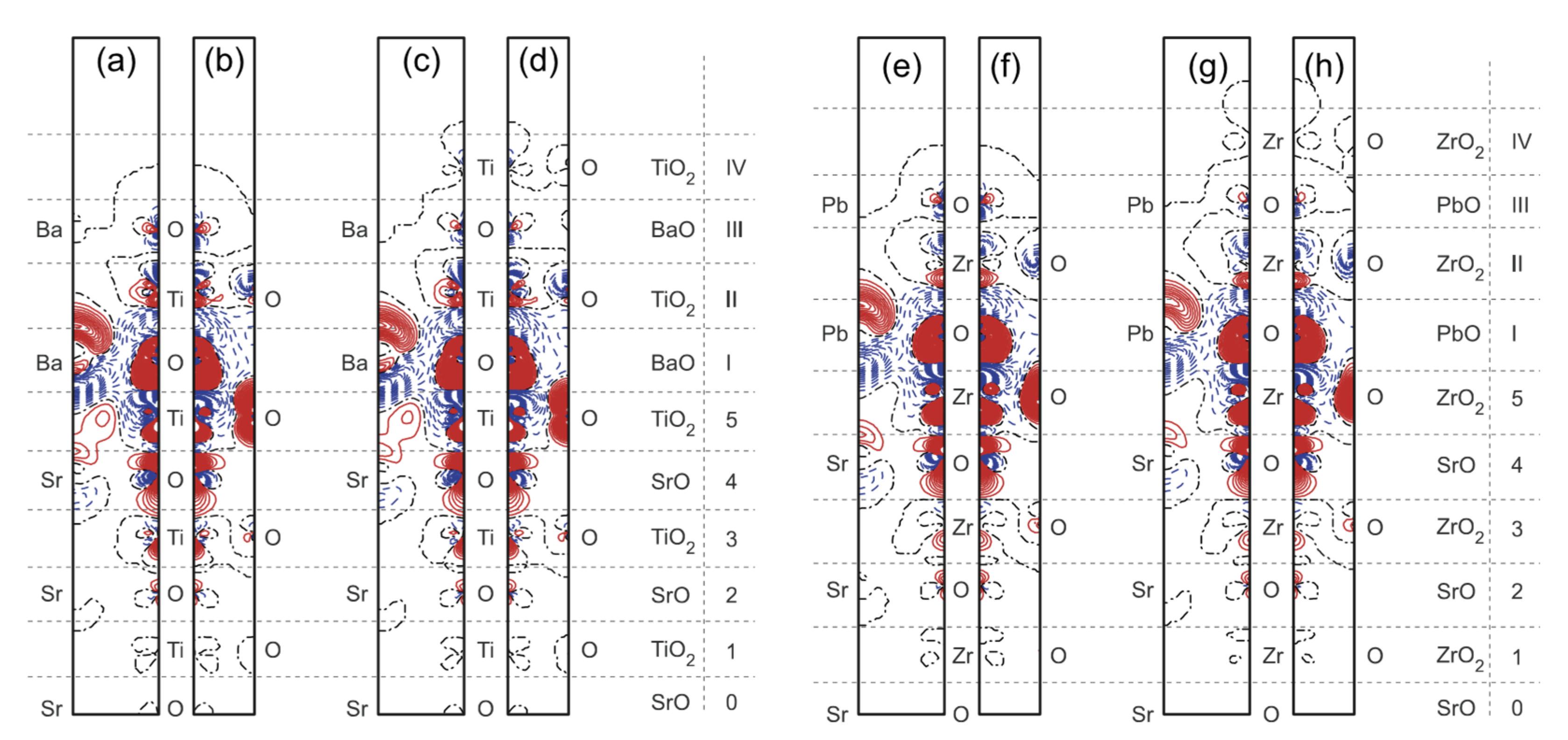
Figure 1.
Profile of the (001) heterostructure between the STO and BTO high-symmetry cubic perovskites [91]. Planes of the STO substrate are numbered using Arabic numerals. In contrast, the augmented BTO (001) film planes are enumerated using Roman numerals. The Arabic numeral 0 describes the central plane, i.e., SrO of the TiO2-terminated, symmetrical STO (001) substrate, consisting of 11 layers.

Figure 2.
Our ab initio B3PW-simulated bulk electronic band structures for PTO (a) and BTO (b) perovskites [142].
Figure 2.
Our ab initio B3PW-simulated bulk electronic band structures for PTO (a) and BTO (b) perovskites [142].

Figure 3.
Our ab initio simulated top-layer atomic shift sizes Δz (% a0) for eleven-layer TiO2-terminated STO (001) substrate (x = 0) and for ten augmented BTO layers (x = 1–10) [77].
Figure 3.
Our ab initio simulated top-layer atomic shift sizes Δz (% a0) for eleven-layer TiO2-terminated STO (001) substrate (x = 0) and for ten augmented BTO layers (x = 1–10) [77].

Figure 4.
Difference electron charge density charts computed for STO/BTO (001) interfaces. (a) (110) cross-section for NBaTiO3 = 3. (b) (100) cross-section for NBaTiO3 = 3. (c) (110) cross-section for NBaTiO3 = 4. (d) (100) cross-section for NBaTiO3 = 4. Blue dashed, red solid, and black dash–dot isolines represent negative, positive, and zero values of difference charge density. Isodensity curves are plotted from −0.025 to +0.025e Å−3 using the increment of 0.0005e Å−3. Right-hand bar shows the atomic monolayer from which the atoms originated. Computations were carried out using the B3PW exchange-correlation functional. STO and BTO monolayers are enumerated starting from the slab center. Monolayers are enumerated one by one for STO (001) substrate and for augmented BTO (001) nano-film by employing Arabic or Roman characters [91].

Figure 5.
Layer-by-layer-projected DOS of 3 UC wide STO/BTO (001) heterostructure computed using the B3PW functional. Energy scale was set with respect to the vacuum level [91].
Figure 5.
Layer-by-layer-projected DOS of 3 UC wide STO/BTO (001) heterostructure computed using the B3PW functional. Energy scale was set with respect to the vacuum level [91].
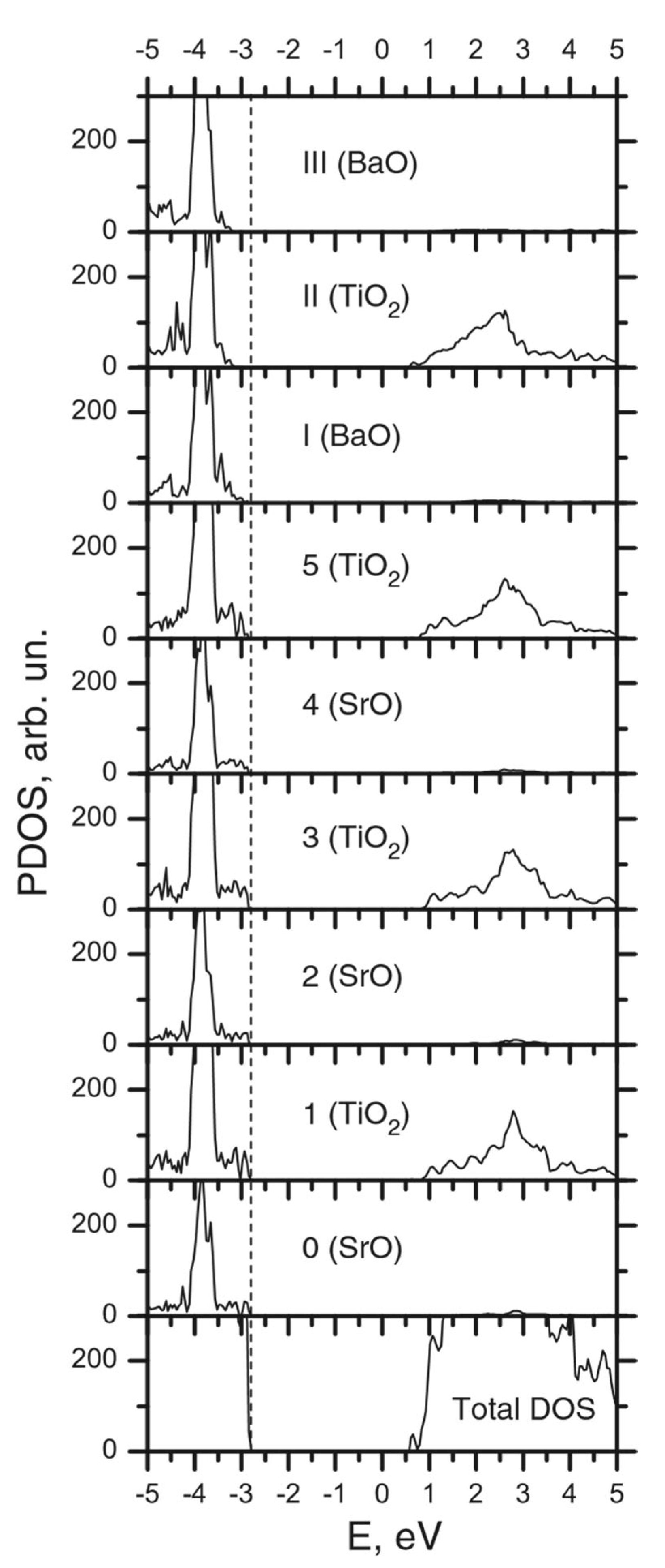
Figure 6.
Layer-by-layer-projected DOS of 4 UC wide STO/BTO (001) heterostructure as computed using the B3PW functional. Energy scale was set with respect to the vacuum level [91].
Figure 6.
Layer-by-layer-projected DOS of 4 UC wide STO/BTO (001) heterostructure as computed using the B3PW functional. Energy scale was set with respect to the vacuum level [91].
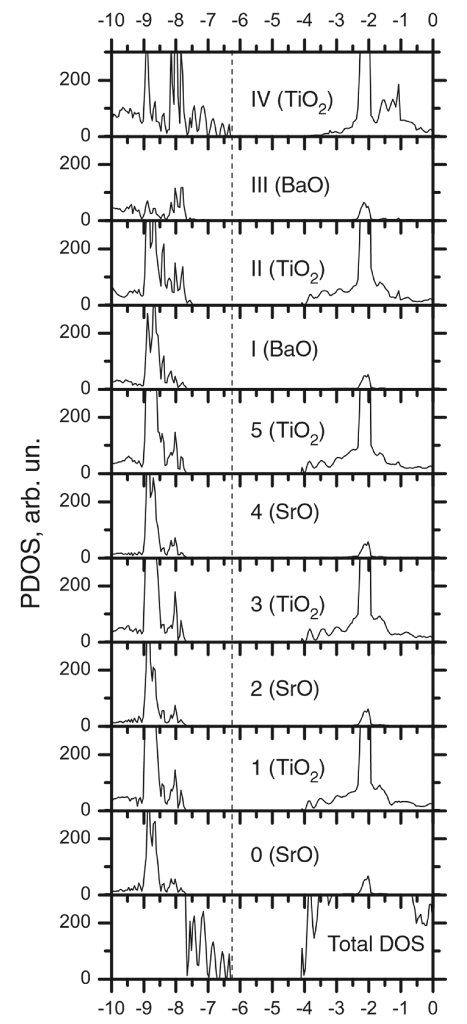
Figure 7.
B3PW-simulated optical band gaps of STO/BTO (001) heterostructures (Table 5). The number of deposited BTO monolayers switches from 0 (TiO2-terminated STO eleven-layer (001) substrate) to 10. Dashed lines serve as a guide for the eyes [91].

Figure 8.
Sketch of the (001) heterostructures between 2 cubic perovskite matrixes: PTO and STO. STO substrate (001) planes are enumerated using Arabic numerals. The Roman numerals are employed for deposited PTO (001) film. We used the Arabic number 0 to represent the central plane of the 11-layer symmetrical TiO2-terminated STO (001) substrate [87].

Figure 9.
First-principles-simulated top-layer atomic shift sizes Δz (% a0) for the eleven-layer STO (001) substrate (x = 0) and ten augmented PTO layers (x = 1–10) [77].
Figure 9.
First-principles-simulated top-layer atomic shift sizes Δz (% a0) for the eleven-layer STO (001) substrate (x = 0) and ten augmented PTO layers (x = 1–10) [77].
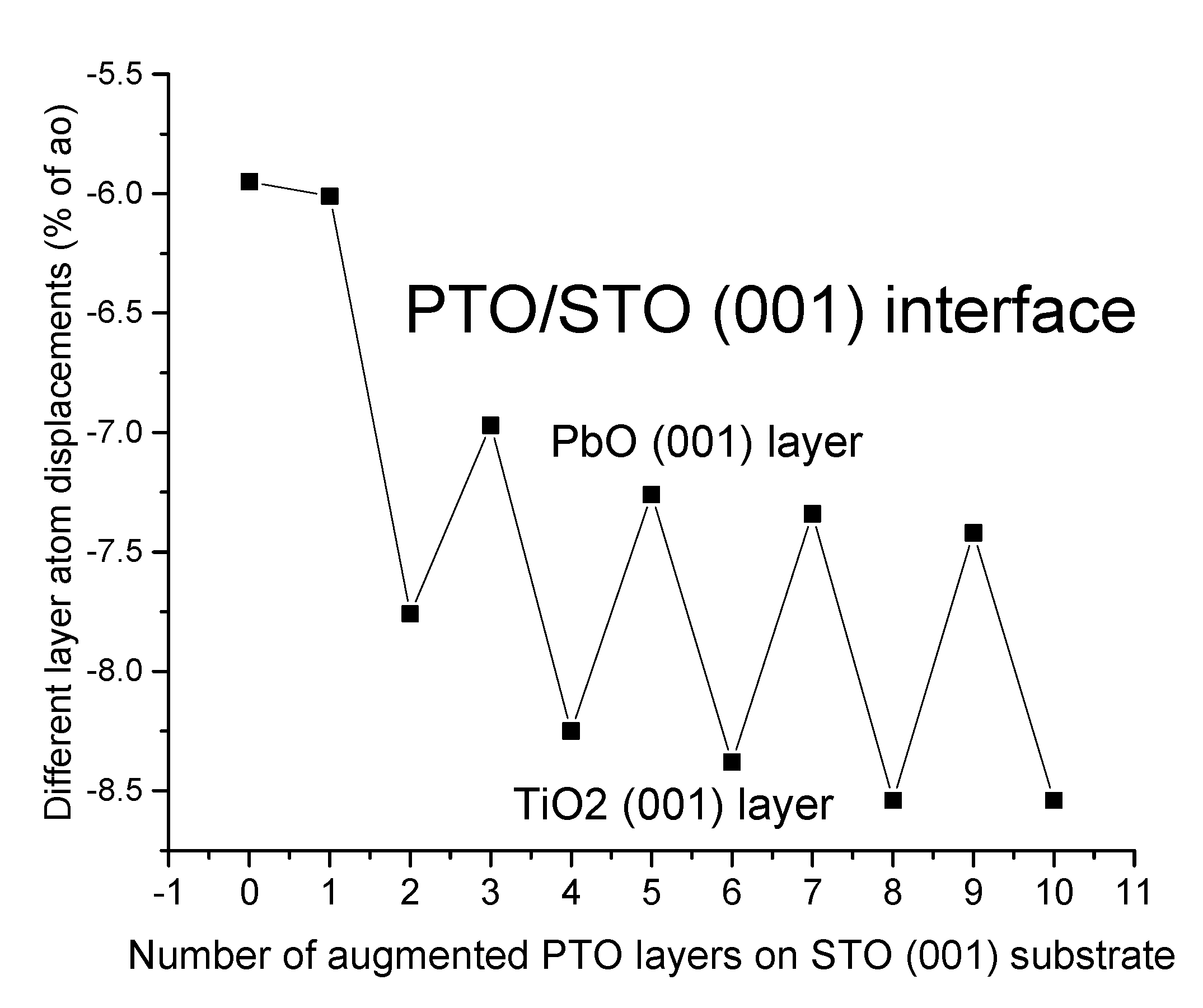
Figure 10.
Our ab initio B3PW-computed difference electron charge density charts for STO/PTO (001) interfaces: (a) (110) cross-section of NPbTiO3 = 3. (b) (100) cross-section of NPbTiO3 = 3. (c) (110) cross-section of NPbTiO3 = 4. (d) (100) cross-section of NPbTiO3 = 4. Blue dashed, red solid, and black dash-dotted isolines present negative, positive, and 0 values of the difference charge density. Isodensity curves were plotted from −0.025 to +0.025e Å−3 with an increment of 0.0005e Å−3. Right-hand bar shows atomic monolayers from which atoms originated. STO and PTO monolayers are enumerated starting from the slab center [87].
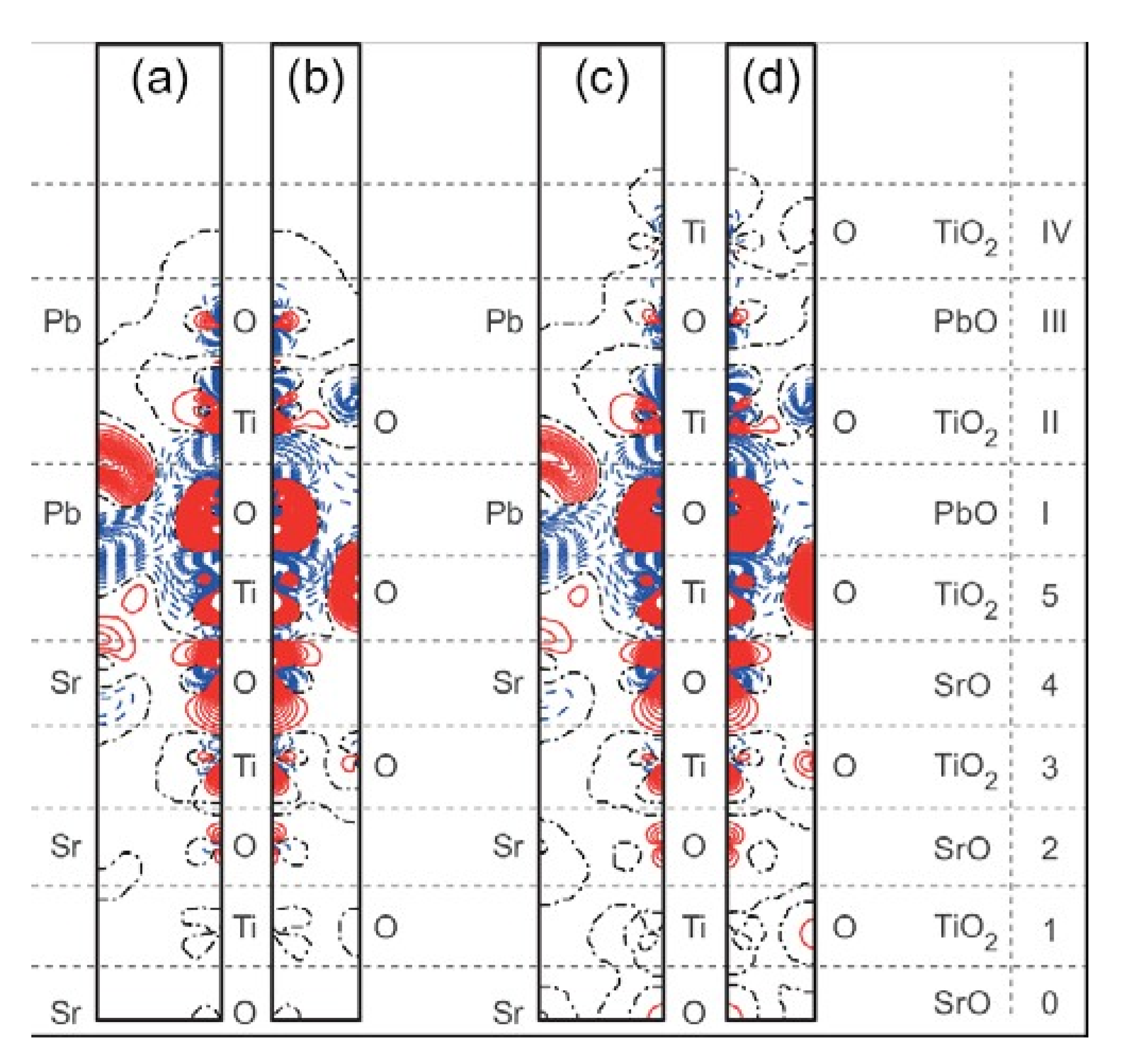
Figure 11.
Ab initio B3PW-computed layer-by-layer-projected DOS of 3 UC thick STO/PTO (001) interfaces. Energy scale is depicted with respect to the vacuum level [87].
Figure 11.
Ab initio B3PW-computed layer-by-layer-projected DOS of 3 UC thick STO/PTO (001) interfaces. Energy scale is depicted with respect to the vacuum level [87].

Figure 12.
Ab initio B3PW-computed layer-by-layer-projected DOS of 4 UC thick STO/PTO (001) interfaces. Energy scale is depicted with respect to the vacuum level [87].
Figure 12.
Ab initio B3PW-computed layer-by-layer-projected DOS of 4 UC thick STO/PTO (001) interfaces. Energy scale is depicted with respect to the vacuum level [87].
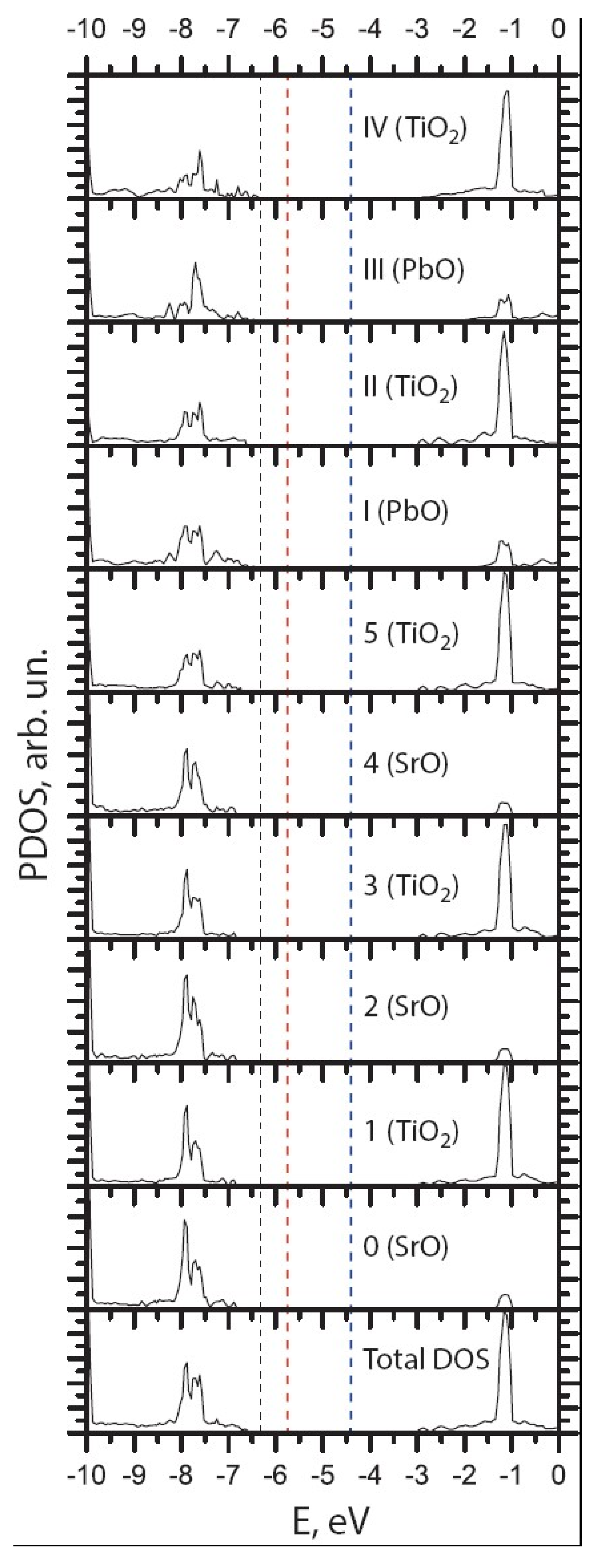
Figure 13.
Ab initio calculated Γ-Γ band gap (in eV) for the STO/PTO (001) heterostructures, as a function of the number of PTO (001) layers, augmented onto the TiO2-terminated STO (001) substrate [77].
Figure 13.
Ab initio calculated Γ-Γ band gap (in eV) for the STO/PTO (001) heterostructures, as a function of the number of PTO (001) layers, augmented onto the TiO2-terminated STO (001) substrate [77].

Figure 14.
Ab initio computed optical band gaps for STO/PTO (001) interfaces, depending on the number of PTO (001) layers (x = 1–10), augmented on the TiO2-terminated STO (001) substrate. Ab initio computed band gaps for STO/BTO and SZO/PZO (001) heterostructures are mentioned for comparative purposes [83].

Figure 15.
Difference electron charge density charts computed for STO/BTO and SZO/PZO (001) interfaces. (a) (110) cross-section for NBaTiO3 = 3. (b) (100) cross-section for NBaTiO3 = 3. (c) (110) cross-section for NBaTiO3 = 4. (d) (100) cross-section for NBaTiO3 = 4. (e) (110) cross-section for NPbZrO3 = 3. (f) (100) cross-section for NPbZrO3 = 3. (g) (110) cross-section for NPbZrO3 = 4. (h) (100) cross-section for NPbZrO3 = 4. Blued dashed, red solid, and black dash-dot isolines describe negative, positive, and zero values of the difference charge density. Isodensity curves are plotted from −0.025 to +0.025e Å−3 with an increase of 0.0005e Å−3. Right-side bar displays the atomic monolayers from which atoms originated [83].

Figure 16.
First-principles-simulated optical band gaps of (a) STO/BTO (001) and (b) SZO/PZO (001) heterostructures. The number of deposited BTO or PZO (001) monolayers varies from 0 (TiO2- or ZrO2-terminated STO or SZO (001) substrate) to 10. Dashed lines serve as a guide for the eyes [83].
Figure 16.
First-principles-simulated optical band gaps of (a) STO/BTO (001) and (b) SZO/PZO (001) heterostructures. The number of deposited BTO or PZO (001) monolayers varies from 0 (TiO2- or ZrO2-terminated STO or SZO (001) substrate) to 10. Dashed lines serve as a guide for the eyes [83].


Table 1.
BaZrO3, MgF2, and CaF2 bulk Γ-Γ band gaps [29,119,120] computed by employing different exchange correlation-functionals. Experimental bulk Γ-Γ band gaps [121,122,123] are listed for illustration.
| Ab initio Method | BZO [29] | MgF2 [119] | CaF2 [120] |
| Experiment | 5.3 [121] | 13.0 [122] | 12.1 [123] |
| B3LYP | 4.79 | 9.42 | 10.85 |
| B3PW | 4.93 | 9.48 | 10.96 |
| HF | 12.96 | 19.65 | 20.77 |
| PWGGA | 3.24 | 6.94 | 8.51 |
Table 2.
Our first-principles B3PW-computed BTO, PTO, STO, SZO, and PZO bulk lattice constants. The experimentally detected respective ABO3 perovskite bulk lattice values are listed for analytical purposes.
Table 2.
Our first-principles B3PW-computed BTO, PTO, STO, SZO, and PZO bulk lattice constants. The experimentally detected respective ABO3 perovskite bulk lattice values are listed for analytical purposes.
| Material | BTO | PTO | STO | SZO | PZO |
|---|---|---|---|---|---|
| Computed | 4.008 | 3.936 | 3.904 | 4.195 | 4.220 |
| Experiment | 4.004 [137] | 3.97 [138] | 3.898 [139] | 4.154 [140] | 4.1614 [141] |
Table 3.
Our ab initio B3PW-computed PTO, BaTiO3, and SrTiO3 perovskite bulk. Γ-Γ band gaps (in eV) and their structures obtained at RT. The experimentally detected Γ-Γ band gaps at RT (in eV) are listed for comparative purposes.
Table 3.
Our ab initio B3PW-computed PTO, BaTiO3, and SrTiO3 perovskite bulk. Γ-Γ band gaps (in eV) and their structures obtained at RT. The experimentally detected Γ-Γ band gaps at RT (in eV) are listed for comparative purposes.
| Perovskite | Structure at Room Temperature | B3PW Γ-Γ Gap | Exp. Γ-Γ Gap |
|---|---|---|---|
| PTO | Tetragonal phase | 4.32 eV | 3.4 eV [121] |
| BTO | Tetragonal ↔ orthorhombic phase at a temperature of 278 K | 3.55 eV | 3.38 eV (// c); 3.27 (⊥ c) [143] |
| STO | Cubic phase | 3.96 eV | 3.75 eV [144] |
Table 4.
Our ab initio B3PW-computed atomic effective charges Q (in e) and bond populations P (in e) in BTO, PTO, STO, SZO, and PZO perovskites.
Table 4.
Our ab initio B3PW-computed atomic effective charges Q (in e) and bond populations P (in e) in BTO, PTO, STO, SZO, and PZO perovskites.
| Ion | Property | BTO | PTO | STO | SZO | PZO |
|---|---|---|---|---|---|---|
| A | Q | 1.79 | 1.35 | 1.87 | 1.88 | 1.30 |
| P | −0.034 | 0.016 | −0.010 | −0.008 | −0.020 | |
| O | Q | −1.39 | −1.23 | −1.41 | −1.33 | −1.12 |
| P | 0.100 | 0.098 | 0.088 | 0.084 | 0.100 | |
| B | Q | 2.36 | 2.34 | 2.35 | 2.13 | 2.07 |
Table 5.
Our ab initio B3PW-computed net atomic charges Qatom (in e), in-plane pure charges Qplane (in e), and degrees of relative in-plane shift Δz (% of a0) regarding the ideal bulk positions of metal atoms and band gaps δ (in eV) of BTO/STO (001) heterostructures [91]. Planes of STO (001) substrate are enumerated using Arabic numerals (Figure 1). In contrast, Roman numerals are employed to enumerate the planes of our deposited BTO (001) film. The numeral zero corresponds to the central plane of the slab (Figure 1).
| Layer | Prop. | STO | BTO1 | BTO2 | BTO3 | BTO4 | BTO5 | BTO6 | BTO7 | BTO8 | BTO9 | BTO10 |
|---|---|---|---|---|---|---|---|---|---|---|---|---|
| X | QTi | 2.30 | ||||||||||
| QO | −1.27 | |||||||||||
| Qplane | −0.23 | |||||||||||
| Δz | −3.92 | |||||||||||
| IX | QBa | 1.75 | 1.76 | |||||||||
| QO | −1.48 | −1.37 | ||||||||||
| Qplane | 0.27 | 0.39 | ||||||||||
| Δz | −2.32 | 4.60 | ||||||||||
| VIII | QTi | 2.30 | 2.37 | 2.36 | ||||||||
| QO | −1.26 | −1.41 | −1.36 | |||||||||
| Qplane | −0.23 | −0.44 | −0.36 | |||||||||
| Δz | −3.84 | 3.65 | 0.65 | |||||||||
| VII | QBa | 1.75 | 1.76 | 1.80 | 1.79 | |||||||
| QO | −1.48 | −1.37 | −1.42 | −1.40 | ||||||||
| Qplane | 0.26 | 0.39 | 0.38 | 0.39 | ||||||||
| Δz | −2.21 | 4.62 | 0.68 | 2.12 | ||||||||
| VI | QTi | 2.30 | 2.37 | 2.36 | 2.36 | 2.36 | ||||||
| QO | −1.26 | −1.40 | −1.36 | −1.38 | −1.37 | |||||||
| Qplane | −0.23 | −0.43 | −0.36 | −0.40 | −0.38 | |||||||
| Δz | −3.70 | 3.69 | 0.74 | 1.88 | 1.50 | |||||||
| V | QBa | 1.75 | 1.76 | 1.80 | 1.79 | 1.79 | 1.79 | |||||
| QO | −1.49 | −1.38 | −1.42 | −1.40 | −1.41 | −1.41 | ||||||
| Qplane | 0.26 | 0.38 | 0.37 | 0.39 | 0.39 | 0.39 | ||||||
| Δz | −2.07 | 4.68 | 0.76 | 2.15 | 1.40 | 1.71 | ||||||
| IV | QTi | 2.30 | 2.37 | 2.36 | 2.36 | 2.36 | 2.36 | 2.36 | ||||
| QO | −1.26 | −1.40 | −1.36 | −1.38 | −1.37 | −1.38 | −1.37 | |||||
| Qplane | −0.22 | −0.43 | −0.36 | −0.40 | −0.38 | −0.39 | −0.39 | |||||
| Δz | −3.55 | 3.73 | 0.83 | 1.92 | 1.57 | 1.57 | 1.63 | |||||
| III | QBa | 1.75 | 1.76 | 1.80 | 1.79 | 1.79 | 1.79 | 1.79 | 1.79 | |||
| QO | −1.49 | −1.39 | −1.43 | −1.41 | −1.41 | −1.41 | −1.40 | −1.41 | ||||
| Qplane | 0.25 | 0.38 | 0.37 | 0.38 | 0.39 | 0.38 | 0.39 | 0.38 | ||||
| Δz | −1.84 | 4.77 | 0.89 | 2.27 | 1.48 | 1.79 | 1.53 | 1.68 | ||||
| II | QTi | 2.29 | 2.37 | 2.35 | 2.36 | 2.36 | 2.36 | 2.36 | 2.36 | 2.36 | ||
| QO | −1.25 | −1.40 | −1.35 | −1.38 | −1.37 | −1.38 | −1.37 | −1.38 | −1.37 | |||
| Qplane | −0.21 | −0.42 | −0.35 | −0.39 | −0.37 | −0.39 | −0.38 | −0.39 | −0.39 | |||
| Δz | −3.20 | 3.83 | 1.03 | 2.04 | 1.72 | 1.69 | 1.75 | 1.60 | 1.71 | |||
| I | QBa | 1.75 | 1.76 | 1.80 | 1.79 | 1.79 | 1.79 | 1.79 | 1.79 | 1.79 | 1.79 | |
| QO | −1.51 | −1.40 | −1.44 | −1.43 | −1.42 | −1.42 | −1.42 | −1.42 | −1.41 | −1.42 | ||
| Qplane | 0.23 | 0.36 | 0.35 | 0.36 | 0.37 | 0.37 | 0.38 | 0.37 | 0.38 | 0.37 | ||
| Δz | −1.54 | 4.87 | 1.02 | 2.35 | 1.53 | 1.84 | 1.55 | 1.70 | 1.51 | 1.64 | ||
| 5 | QTi | 2.29 | 2.37 | 2.35 | 2.36 | 2.36 | 2.36 | 2.36 | 2.36 | 2.36 | 2.36 | 2.36 |
| QO | −1.29 | −1.41 | −1.38 | −1.40 | −1.39 | −1.40 | −1.40 | −1.40 | −1.40 | −1.40 | −1.40 | |
| Qplane | −0.30 | −0.45 | −0.40 | −0.44 | −0.42 | −0.44 | −0.43 | −0.44 | −0.44 | −0.45 | −0.44 | |
| Δz | −5.95 | 1.96 | −1.13 | −0.11 | −0.46 | −0.47 | −0.43 | −0.56 | −0.48 | −0.61 | −0.53 | |
| 4 | QSr | 1.85 | 1.88 | 1.87 | 1.87 | 1.87 | 1.87 | 1.87 | 1.87 | 1.87 | 1.87 | 1.87 |
| QO | −1.37 | −1.41 | −1.39 | −1.38 | −1.38 | −1.37 | −1.38 | −1.37 | −1.37 | −1.36 | −1.37 | |
| Qplane | 0.48 | 0.47 | 0.48 | 0.50 | 0.49 | 0.50 | 0.50 | 0.51 | 0.50 | 0.51 | 0.50 | |
| Δz | 4.13 | −1.32 | 0.60 | −0.43 | −0.10 | −0.39 | −0.26 | −0.43 | −0.33 | −0.47 | −0.37 | |
| 3 | QTi | 2.35 | 2.36 | 2.36 | 2.36 | 2.36 | 2.36 | 2.36 | 2.36 | 2.36 | 2.36 | 2.36 |
| QO | −1.38 | −1.42 | −1.41 | −1.42 | −1.41 | −1.42 | −1.42 | −1.43 | −1.42 | −1.43 | −1.42 | |
| Qplane | −0.42 | −0.48 | −0.45 | −0.48 | −0.47 | −0.49 | −0.48 | −0.49 | −0.48 | −0.49 | −0.49 | |
| Δz | −0.96 | 0.27 | −0.20 | −0.25 | −0.21 | −0.38 | −0.29 | −0.44 | −0.35 | −0.48 | −0.40 | |
| 2 | QSr | 1.87 | 1.87 | 1.87 | 1.87 | 1.87 | 1.87 | 1.87 | 1.87 | 1.87 | 1.87 | 1.87 |
| QO | −1.42 | −1.40 | −1.41 | −1.39 | −1.40 | −1.39 | −1.39 | −1.38 | −1.39 | −1.38 | −1.39 | |
| Qplane | 0.45 | 0.47 | 0.46 | 0.48 | 0.47 | 0.49 | 0.48 | 0.49 | 0.48 | 0.49 | 0.49 | |
| Δz | 0.88 | −0.35 | 0.12 | −0.29 | −0.15 | −0.37 | −0.26 | −0.42 | −0.32 | −0.45 | −0.37 | |
| 1 | QTi | 2.35 | 2.36 | 2.36 | 2.36 | 2.36 | 2.36 | 2.36 | 2.36 | 2.36 | 2.36 | 2.36 |
| QO | −1.40 | −1.42 | −1.41 | −1.42 | −1.42 | −1.42 | −1.42 | −1.43 | −1.42 | −1.43 | −1.42 | |
| Qplane | −0.44 | −0.47 | −0.46 | −0.48 | −0.47 | −0.49 | −0.48 | −0.49 | −0.48 | −0.49 | −0.49 | |
| Δz | 0.14 | −0.09 | −0.01 | −0.27 | −0.17 | −0.36 | −0.26 | −0.42 | −0.33 | −0.46 | −0.37 | |
| 0 | QSr | 1.87 | 1.87 | 1.87 | 1.87 | 1.87 | 1.87 | 1.87 | 1.87 | 1.87 | 1.87 | 1.87 |
| QO | −1.42 | −1.40 | −1.41 | −1.39 | −1.40 | −1.39 | −1.39 | −1.38 | −1.39 | −1.38 | −1.39 | |
| Qplane | 0.45 | 0.47 | 0.46 | 0.48 | 0.47 | 0.49 | 0.48 | 0.49 | 0.48 | 0.49 | 0.49 | |
| Δz | 0.00 | 0.00 | 0.00 | 0.00 | 0.00 | 0.00 | 0.00 | 0.00 | 0.00 | 0.00 | 0.00 | |
| δ | 2.58 | 3.47 | 2.33 | 3.29 | 2.16 | 3.25 | 2.10 | 3.24 | 2.06 | 3.22 | 2.06 |
Disclaimer/Publisher’s Note: The statements, opinions and data contained in all publications are solely those of the individual author(s) and contributor(s) and not of MDPI and/or the editor(s). MDPI and/or the editor(s) disclaim responsibility for any injury to people or property resulting from any ideas, methods, instructions or products referred to in the content. |
© 2023 by the authors. Licensee MDPI, Basel, Switzerland. This article is an open access article distributed under the terms and conditions of the Creative Commons Attribution (CC BY) license (https://creativecommons.org/licenses/by/4.0/).
Share and Cite
MDPI and ACS Style
Eglitis, R.I.; Bocharov, D.; Piskunov, S.; Jia, R. Review of First Principles Simulations of STO/BTO, STO/PTO, and SZO/PZO (001) Heterostructures. Crystals 2023, 13, 799. https://doi.org/10.3390/cryst13050799
AMA Style
Eglitis RI, Bocharov D, Piskunov S, Jia R. Review of First Principles Simulations of STO/BTO, STO/PTO, and SZO/PZO (001) Heterostructures. Crystals. 2023; 13(5):799. https://doi.org/10.3390/cryst13050799
Chicago/Turabian StyleEglitis, Roberts I., Dmitry Bocharov, Sergey Piskunov, and Ran Jia. 2023. "Review of First Principles Simulations of STO/BTO, STO/PTO, and SZO/PZO (001) Heterostructures" Crystals 13, no. 5: 799. https://doi.org/10.3390/cryst13050799
Note that from the first issue of 2016, this journal uses article numbers instead of page numbers. See further details here.