1. Introduction
The microstructure of CdS
1−xSe
x-based films and their most important properties (photoconductivity, luminescence, etc.) depend largely on the type and concentration of precursors, film production technology, and thermal activation of photoconductivity [
1,
2,
3,
4]. During thermal activation, the crystallites of films are oxidized, as a result of which, an oxide phase–semiconductor barrier is formed on their surface, the parameters of which can be controlled by optimizing the processing temperature range and the gas medium composition, as well as the composition of the applied pastes.
Materials based on A
2B
6 compounds are developed as basic materials for photoreceiving and emitting structures designed for devices operating in the visible and near infrared range. The use of solid solutions found between these binary compounds, the doping of binary compounds, and solid solutions based on them having various impurities allow modifying the properties of these materials and significantly expanding the possibility of their use. The interest in establishing the relationships between the composition and the structure of the materials, including their properties, is primarily provoked by the need for a reasonable choice of the composition and technology used for producing materials with an optimal combination of properties. Additionally, the patterns of change in composition and microstructure properties can provide valuable information on the behavior of impurities and defects originating in the materials. Semiconductor materials can be obtained the most easily and cheaply in the form of polycrystalline films, so clarifying the above patterns for polycrystalline films is an urgent task [
2,
3].
Polycrystalline films based on CdS
1−xSe
x (0 ≤ x ≤ 1) under certain conditions of preparation have high photoconductivity at room and close to room temperatures and, thus, attract the attention of material engineers and manufacturers of new devices, in particular, manufacturers of solar panels and photoresistors [
3,
4].
In most cases, ceramic or polycrystalline materials are found in the composition of homo- or heterostructures, obtained by pressing and then by heat treatment; vacuum technologies and gaseous epitaxy are used to make photoconductive devices. One of the disadvantages of these technologies is the high cost of equipment and the labor intensity of technical processes. In this regard, the current scientific and technical task is to create a low-cost technology for obtaining materials without quality losses (functional properties) [
5,
6]. One way to solve this is to obtain polycrystalline films A
2B
6 of high quality using alternative, cheaper technologies, such as the method of spraying a suspension supplemented by additional heat treatment, chemical precipitations from solutions, or using various printing methods (screen, jet, and die stamping). These technologies include the screen-printing method, which has several advantages. In particular, it allows combining the locality of the film deposition and the possibility of varying their composition on the surface and within their thickness (from 30 μm to 5 μm) [
7,
8]. The ability of the method to produce cheap polycrystalline films of almost any required area per cycle makes it potentially suitable for the production of photodetector devices, as well as for the development of new converter designs using large-area films on surfaces of different curvatures [
9]. The developed screen-printing method provides the formation of polycrystalline films of a given area per cycle, allowing to vary their thickness from tens of microns to units, which makes it possible to reduce the solar cell thickness and facilitate the process of its adhesion/contact to the substrate [
10,
11].
According to the literature sources, A
2B
6 compounds are wide-bandgap semiconductors. The boundaries of the homogeneity region of cadmium sulfides and selenide are retrograde. Cadmium sulfides and selenide are capable of forming a continuous series of solid solutions in the CdS–CdSe system [
12,
13]. This is due to the uniformity of the crystal structures of the components (wurtzite), the proximity of the parameters of their elementary cells, and the close iconicity values of CdS and CdSe [
14].
The photovoltaic properties of A
2B
6 compounds, which are structure-sensitive, are determined by both the crystal structure and its imperfections: defects in the crystal lattice. The effect of defects on the structure-sensitive properties of A
2B
6 compounds are studied separately. The predominant majority of studies are devoted to point defects, which make the greatest contribution to the formation of optoelectronic properties of these compounds. The effect of dislocations on the optoelectronic properties of A
2B
6 compounds is studied to a lesser extent. The presented data show that in the scientific literature, there is still no clear understanding of the nature of the predominant defects appearing in CdS and CdSe when the composition deviates from stoichiometric ones [
15,
16].
The chemical state of the surface of semiconductor materials of the A
2B
6 group was studied mainly only by X-ray and thermogravimetric methods. Therefore, the studies conducted so far have revealed the impact of oxygen on the semiconductor properties of A
2B
6 compounds (dark conductivity is especially sharply affected), but the question about the structure of oxygen centers remains controversial [
12,
13].
A small number of works are devoted to the study of the oxidation of A
2B
6 compounds when doping bulk materials and films with oxygen in order to change electro-physical properties, as well as to study the processes occurring while thermally treating materials in air [
17,
18].
According to the literature sources, CdS
1−xSe
x films can be obtained by several methods that can be divided into two groups: (1) traditional ones, involving the condensation from the gas phase, precipitation from solutions, and pulverization method, and (2) nontraditional, such as various printing methods (screening, jet printing, and die stamping) [
19,
20].
Traditional methods producing polycrystalline CdS
1−xSe
x films (MOCVD, vacuum methods, and film-forming solution pulverization) require using expensive equipment and materials; they are energy-intensive, and in some cases, they are characterized by low photovoltaic parameters. The screen-printing method, as reported in the literature, can become an alternative to traditional technologies for producing polycrystalline CdS
1−xSe
x films. However, it is necessary to solve a number of problems aimed at improving the phase composition, microstructure, and photovoltaic characteristics of films by choosing the optimal conditions favorable for preparing and applying pastes, as well as for activating photosensitivity [
21,
22]. It allows combining the coating locality and the possibility of the simultaneous formation of sections having different compositions on films, thus providing high functional characteristics [
23].
One important point in the formation of the photosensitivity in polycrystalline films is the choice of a substrate material [
24,
25]. In the scientific literature, glass, or ceramic or polycrystalline glasses, are known to be the most often used as substrates. According to the combination of dielectric and mechanical properties, surface microrelief, and chemical resistance, the most acceptable material for screen-printing substrates is polycrystalline glass [
2,
3].
Their microstructure and the most important properties (photoconductivity, luminescence, etc.) are known to depend more on the concentration of the precursors, technology, and photoconductivity thermal activation at temperatures of 800–900 K. The photosensitivity of these films depends on the annealing time in air, increasing along with annealing time increase, reaching the maximum value during annealing for 10–20 min, and then decreasing in the course of a longer heat treatment [
26,
27].
However, the advantages of this method can be realized only by solving a number of synthetic and technological problems related, in particular, to providing the final product purity, controlled formation of the films of the required composition and structure, and development of a controlled process for activating the photosensitivity of the polycrystalline films.
In view of this, the aim of this work was to study the morphological peculiarities of the polycrystalline CdS1−xSex films obtained by the optimized screen-printing method and to create a model of the process of their formation.
As a result of the work, based on the obtained experimental data, a model of the film formation process was developed. The model validity was justified by the conformity of the data of the experiment performed on its basis. The developed screen-printing method provides the formation of the polycrystalline films of a specified area per cycle if the variation of their thickness from tens of microns to units is possible, allowing to reduce the solar cell thickness and facilitating the process of its connection with the substrate.
2. Materials and Methods
This work proposes using a set of methods that allow studying the microstructure in detail: the shape and average size of crystallites, states of intergranular boundaries, porosity, relief (by means of optical microscopy and electron microscopy (scanning (SEM)), the chemical and phase composition of films (X-ray photoelectron spectroscopy (XPS)), and X-ray electron probe analysis (EMPA and XRD).
Optical microscopy was used to characterize the microstructure and morphological features of the studied films and to determine their thickness. A binocular microscope “MBS-10” (7–109× magnification) and an interference microscope “MII-4” (490× magnification) were used in the study.
In this work, scanning electron microscopy was performed using SUPRA 50 VP microscopes made by LEO (Carl Zeiss, Oberkochen, Germany) and JEOL JSM 6490 LV (JEOL, Tokyo, Japan). Both microscopes are equipped with an energy dispersion analyzer, conforming to standards and software. To remove the electrostatic charge, and thereby increase the image clarity, carbon conductive adhesive was applied to the film edge.
The local X-ray electron probe analysis (EMPA) was used to determine the composition of films. The analysis was performed on a SUPRA 50 scanning microscope at 5000–50,000× magnification, using a Jeol JSM 6490LV (JEOL, Tokyo, Japan). The samples were attached to the holder using double-sided conductive tape.
The X-ray photoelectron spectra were recorded on the ES-CALABMK-II spectrometer (Thermo Fisher Scientific, Waltham, MA, USA). To analyze the samples, the panoramic spectrum in the 0–1225 eV binding energies was first 0.1 eV steps at 50 eV analyzer energies. After performing the calibration, the energies of photoelectronic and Auger peaks of the standards differed from the reference data by no more than 0.1 eV [
28,
29].
To take into account the possible recharging of the surface, an external standard method was used, which is based on using a layer of hydrocarbon pollutants arising from the evaporation and subsequent condensation on the surface of the diffusion pump oil sample. The electron binding energies in such a surface layer for the C 1s line are sufficiently stable to be 285.0 ± 0.2 eV.
XRD was conducted for both initial powders and films after heat treatment. The molar ratio was determined in both cases. Since cadmium sulfide has a greater vapor elasticity than selenide does, some more CdS is lost during the preliminary synthesis of the solid solution and subsequent heat treatment of the films, as a result of which the composition of the solid solution is changed towards selenide.
Two problems were solved in this work using the X-ray diffraction method: the definition of the phase composition of the samples and the molar composition of the solid solution. X-ray diffractograms of the powders were recorded on a Huber diffract meter, with silicon as an internal standard and a coordinate detector for recording reflected pulses. X-ray diffractograms of the films were recorded on a D8 diffractometer by Bruker. In both cases, Cu K
α1 radiation was used [
30].
The following data collection modes were used: 2Θ ÷10 − 80º for the powders and 2Θ ÷15 − 80º for the films. The maximum intensity of the reflexes for the powders was ÷5000 − 8000 pulses and 8000–12,000 pulses for the films. In this mode, we were able to see impurity phases in the main powder at a level of less than 0.3 wt%. X-ray patterns were processed using the standard X-Power method and the PDF-2 database.
The molar content of the components in the samples was determined by concentration relationships of the parameters of the elementary cells of solid solutions. The accuracy of the radiographic method was up to ±0.002.
The texture of the CdS1−xSex films was also determined by X-ray diffraction method. To this end, line intensities having the same indices (hkl) were compared using X-ray diffraction patterns of the synthesized films, bulk cadmium sulfides, and selenide.
Polycrystalline films CdS1−xSex were made according to the following scheme: a mixture of cadmium sulfide and selenide powders, as well as copper hydrochloride and cadmium, was preliminary sintered; then, the sinter was ground and mixed with the binder. CdS and CdSe powders of the ACS qualification were used to prepare pastes.
One of the main criteria for selecting alloying impurities was the possibility of the flexible and controlled monitoring of the semiconductor material properties. When doping cadmium chalcogenides, Cu is most often used as an acceptor impurity, and Cl is used as a donor impurity. To obtain certain characteristics, complex alloying is often used, i.e., simultaneous doping with a donor and acceptor impurity is carried out.
The form in which the alloying impurity is introduced also plays an important role. The alloying agent must not contain components capable of introducing contamination into the alloyed material. Hence, when alloying the considered compounds with copper, the use of such compounds as CuO, Cu(NO3)2, and CuCO3 can result in the additional alloying or contamination of the films with impurity phases, which is extremely undesirable.
On the contrary, usingCdCl2 as a flux, consisting of atoms of the main component and an alloying impurity when synthesizing the films, eliminates the probability of the formation of any supplementary phases, and thereby contributes to the preservation of the semiconductor material’s “purity”. Considering this fact in this work, Cu(OH)Cl was chosen as an alloying agent, with CdCl2·H2O as a flux. Nitrocellulose was used as an organic binder, and propylene glycol was applied as a solvent. The paste was applied using a stencil (200–500 mesh) on a polycrystalline glass substrate, after which it was dried at 310–340 K and then subjected to heat treatment accompanied by a limited air access at 821–870 K for 30–60 min. The diagnostics of intermediates and films was performed on a SUPRA 50 VP electron microscope and an X-ray Bruker diffractometer; the oxidized surface of CdS1−xSex films was studied by X-ray photoelectron spectroscopy using the ESCALABMK-II spectrometer.
The CdS
1−xSe
x films were applied to the polycrystalline glass substrate by screen printing according to the scheme shown in
Figure 1.
After the paste is applied to the substrate, the freshly printed pattern represents a plurality of separate points, the positions of which correspond to the open cells of the template (
Figure 1). When the substrate is held for several minutes under normal conditions, the paste particles merge, and a solid even film is formed (
Figure 1). The time required for particles to join depends on the paste composition. At this stage of manufacturing the film, the most important printing characteristics are the film thickness and pattern clarity. The film thickness in operation was controlled by sieve density. Synthetic (nylon) or metal (stainless steel) sieves were used. The thicknesses of the finished films was 15 and 7 μm, respectively.
The CdS
1−xSe
x films were applied to a sitall substrate by screen printing according to the scheme shown in
Figure 1 (stage 1–2). After applying the paste onto the substrate, the freshly printed drawing represents a set of individual points whose position corresponds to the open holes of the stencil (
Figure 1, stage 3). When the substrate is held for several minutes under normal conditions, the paste particles merge, and a solid, even film is formed (
Figure 1, stage 4). The time required to connect the particles depends on the paste composition.
At this stage of film production (application and drying of the paste on the substrate), the following parameters were varied: the size of the gap between the stencil and the substrate and the drying conditions of the films after application. The most important characteristics of printing are the film thickness and pattern clarity. At the stage of producing the films, their thickness was controlled by the density of the sieves.
3. Results and Discussion
The experimental studies [
1,
2,
3] showed that the modes of applying the films onto the polycrystalline glass substrates by screen printing, while choosing a particular web to apply the paste to a substrate, require considering the functional purpose of the applied film. The size of the gap between the stencil and the substrate was selected by varying the sizes of the gap (0.5–4 mm) between the stencil and the substrate during the film deposition.
Figure 2 shows the microstructure of the films applied at different spacings between the stencil and the substrate. The figure shows that when the gap between the stencil and the substrate increases to 4–6 mm, there is spreading (A), an uneven edge (B), and an edge plate (C) on the surface of the films, and reducing the gap to 0.5–2 mm allows seeing a grid pattern (D) and punctures from the grid (E). The average interval between these values of 1–3 mm made it possible to obtain films without defects (
Figure 3e).
At the stage of film production, the density of the sieves controlled their thickness. Obtaining the films without printing defects demands providing a sieve tension of 45–50 N/cm and a gap between the stencil and the substrate ranging from 1 to 2 mm. In this work, the profilometry method (profilometer by Taylor-Nobson (Leicester, UK)) was used to quantify the thickness of the film, changes in its microstructure, and relief. Profilometry is a method for determining irregularities on the surface of nanoscale samples. A thin needle was used as a measuring device, moving at a certain distance under the action of a fixed voltage in the measuring unit of the device. During measurements, the voltage increases until the moment when the needle touches the sample surface. The distance the needle moved is determined by the voltage under which the needle reaches the sample surface. The diameter of the measuring needle is 0.1 mcm, and the measurement step is 0.4 mcm. The 2–3 linear profilograms were taken on each film in different parts of the sample. The measurement path in all the cases is 1 mm. According to the conducted research, it was found that the surface of the CdS1−xSexfilms has a developed relief. It can be described as a system of “valleys”, i.e., the film sections have a thickness of 1–4 mcm less than the average film thickness, and “protrusions”, i.e., the film sections protruding above the surface. There is no system in the extension height (depth) of the “protrusions” (“valleys”).
In order to determine the effect of the heat treatment modes on the microstructure and composition of the films, the parameter, such as the composition of the atmosphere in the reactor of the furnace, was varied during the experiment, in addition to the temperature and elongation of annealing.
Three heat treatment methods were used in the study: heat treatment permitting free access of air oxygen, heat treatment in a nitrogen atmosphere, and heat treatment in a titanium container (quasi-closed volume).
To monitor the oxidation process, the heat treatment of the films allowing free air access was conducted for 15 min at a temperature of 835 K.
The studies showed that the heat treatment of the CdS
1−xSe
x films provided with free oxygen access led to complete oxidation of their surface. At the beginning of the heat treatment process, small islands of the rounded form of the oxide phase appear at the defective places of the film (microcracks, pores, and grain boundaries). After that, being oxidation centers, they quickly grow and cover half of the film surface, which is confirmed by the formation of gray spots on the surface of the films (
Figure 3).
Therefore, it was established that obtaining the films without printing defects requires providing a gap between the stencil and the substrate, ranging from 1 to 3 mm.
To clarify the temperature range in which the film will be oxidized, we conducted a study on the oxidation of CdS and CdSe powders and solid solutions of CdS1−xSex (x = 0; 0.2; 0.8) by TGA method. The samples were heated in air to a temperature of 1070 K at a speed of 10 K/min.
According to the TGA data, the oxidation of cadmium sulfide begins at a temperature of 780 (±5) K and cadmium selenide at 680 (±5) K. Along with the oxidation process, decomposition probably proceeds in the samples: sulfate is decomposed at temperatures of 880–1050 (±5) K, and cadmium selenite is broken down at temperatures of 880–990 (±5) K. The decomposition process becomes predominant in the case of cadmium sulfide when heated above 1050 (±5) K, and it is above 990 (±5) K for cadmium selenide. The obtained values of the temperatures of the beginning of the oxidation and decomposition processes confirm the literature data. In the case of a solid solution, the existence area of the oxidized phase is wider. The oxidation of the CdS1−xSex solid solutions, according to TGA data, begins at a temperature of 700 (±5) K, and the decomposition is initiated at a temperature above 900 K. To observe the oxidation process, the films having free air access were thermally treated for 10–30 min at a temperature of 823–867 K in a high-temperature microscope furnace.
As studies have shown, such heat treatment of the films leads to a complete oxidation (degradation) of their surface. First, small islands of a rounded shape of the oxide phase appear in the defective places of the film (microcracks, pores, and grain boundaries). Then, serving as oxidation centers, they grow rapidly and completely cover the film surface, as evidenced by the formation of gray spots on the surface of the films.
When annealing the films, along with recrystallization processes, oxide phases are formed. Such processes proceed intensively in the films at temperatures of 670–870 K, which is confirmed by the results of microscopic and X-ray studies, including X-ray photoelectron spectroscopy (XPES).
The electron microprobe analysis (EMPA) of the films, annealed using a different access of oxygen in the air, showed that the composition of the films is sufficiently uniform in the area. In addition to the main paste elements (Cd, S, and Se), the films contain a significant amount of oxygen, whose concentration in the finished films increases in proportion to the increase in the oxygen concentration in the furnace reactor during heat treatment. The heat treatment of the films by method 2 is shown to reduce the acid content in them by 40–50%.
Studies on the microstructure, composition, and photovoltaic properties of the films after their heat treatment in a nitrogen atmosphere showed that such heat treatment produced samples with a good microstructure and no impurity phases but without photosensitivity.
The XPA of the films showed that the phase composition of the samples annealed in air was complex. The vast majority of the lines are identified. They belong to the hexagonal modification of cadmium sulfide or CdS1−xSex solid solutions; furthermore, the cubic modification of CdS, sulfate, silicate, and cadmium oxide are also found.
Based on this fact, the photoelectric properties of the films are assumed to be influenced by air oxygen, which is confirmed by the literature data [
1,
2,
3]; therefore, in the future, the films will be heat treated in a diffusion furnace SDO-125/4 with limited access to air oxygen (quasi-closed volume). The films were placed in a titanium container and covered with a lid. A gap remained between the container and the lid, permitting the air oxygen supply.
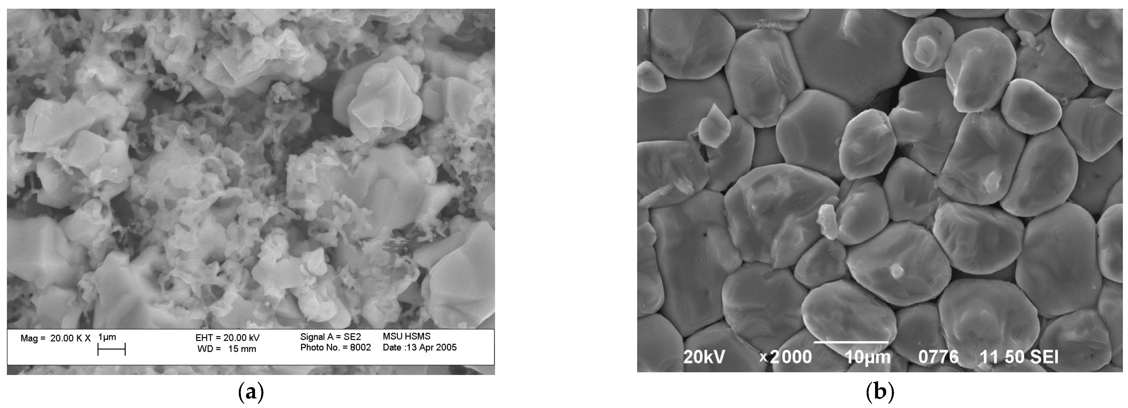
Figure 4 shows the microstructure of the CdS
1−xSe
x films annealed under different air access conditions. The figure shows that the films differ in the shape and size of the grains and voids in the intergranular space.
The crystals with a round polyhedral shape (
Figure 4b) characterize the films that were treated with heat in a quasi-closed volume. The comparison of photos “a” and “b” shows that the air restriction to the furnace reactor leads to the enlargement of crystallites, polygenation (bonding) of individual grains, and a decrease in film damage.
As the selenium content in the solid solution increases, it becomes elongated. In case of such thermal activation, the films with a grain size of 5 to 10 μm and small thickness are obtained. The increase in the structural quality of the films can be explained by the decrease in the negative effect produced on the movement of the intergranular boundaries of the air oxygen crystallites. That is, the process of bonding the crystallites and their coarsening is facilitated with a simultaneous increase in the structural quality of the films, small thickness, and leveling of the relief.
According to XRD, the polycrystalline CdS1−xSex films were single-phase; no impurity phases were found. Under these heat treatment conditions, films with some amount of roughness are obtained. They are characterized by the following parameters: the average height of the protrusions was 3–4 µm, and the average pore depth was 1–5 µm. In the case of the polycrystalline CdS1−xSex films obtained by screen printing, crystallites of the round polyhedral shape are typical; when the selenium content increases in the solid solution, it acquires an elongated shape—it is sufficiently densely packed with well-formed grain boundaries and low porosity.
To establish the influence of cooling modes on the microstructure of the films, two cooling modes were tested: rapid cooling of the film (20 min, υ = 3 K/min) and cooling of the film along with the furnace (180 min, υ = 30 K/min). A decrease in the cooling rate of the films after heat treatment was found to act in the same way as an increase in the temperature of the heat treatment to 823 K or its duration to 15–30 min does. That is, it leads to the formation of crystallographic-cut grains on the surface of the film grains and a decrease in the light resistance value.
When the film is cooled to 673 K, the crystallization process is fully completed. The width of the lines at half-height on the X-ray films decreases from 0.19 to 0.07 degrees (
Table 1).
During the oxidation of the films in air, the surface quality deteriorates due to gas etching. That is, the CdSO
3 formed at the first moment of oxidation decomposes, accompanied by the release of SO
2, which is confirmed by the results of XRD (
Figure 5, line 1). In the case of a quasi-closed volume, during heat treatment, an equilibrium is established in the container between cadmium sulfite and sulfur and cadmium oxides; so, cadmium sulfite is further oxidized to cadmium sulfate, which is more stable at these heat treatment temperatures. This can be confirmed by the data of the XRD (
Figure 5, line 2, 3) and XPS (
Figure 6). The XRD of the films showed that the phase composition of the samples annealed by air was complex. The vast majority of lines are identified (
Figure 5). They belong to the hexagonal modification of cadmium sulfide or solid solutions CdS
1−xSe
x; in addition, sulfate, silicate, and cadmium oxide are also found.
The oxidation processes of solid solutions CdS1−xSex appear to follow a similar mechanism.
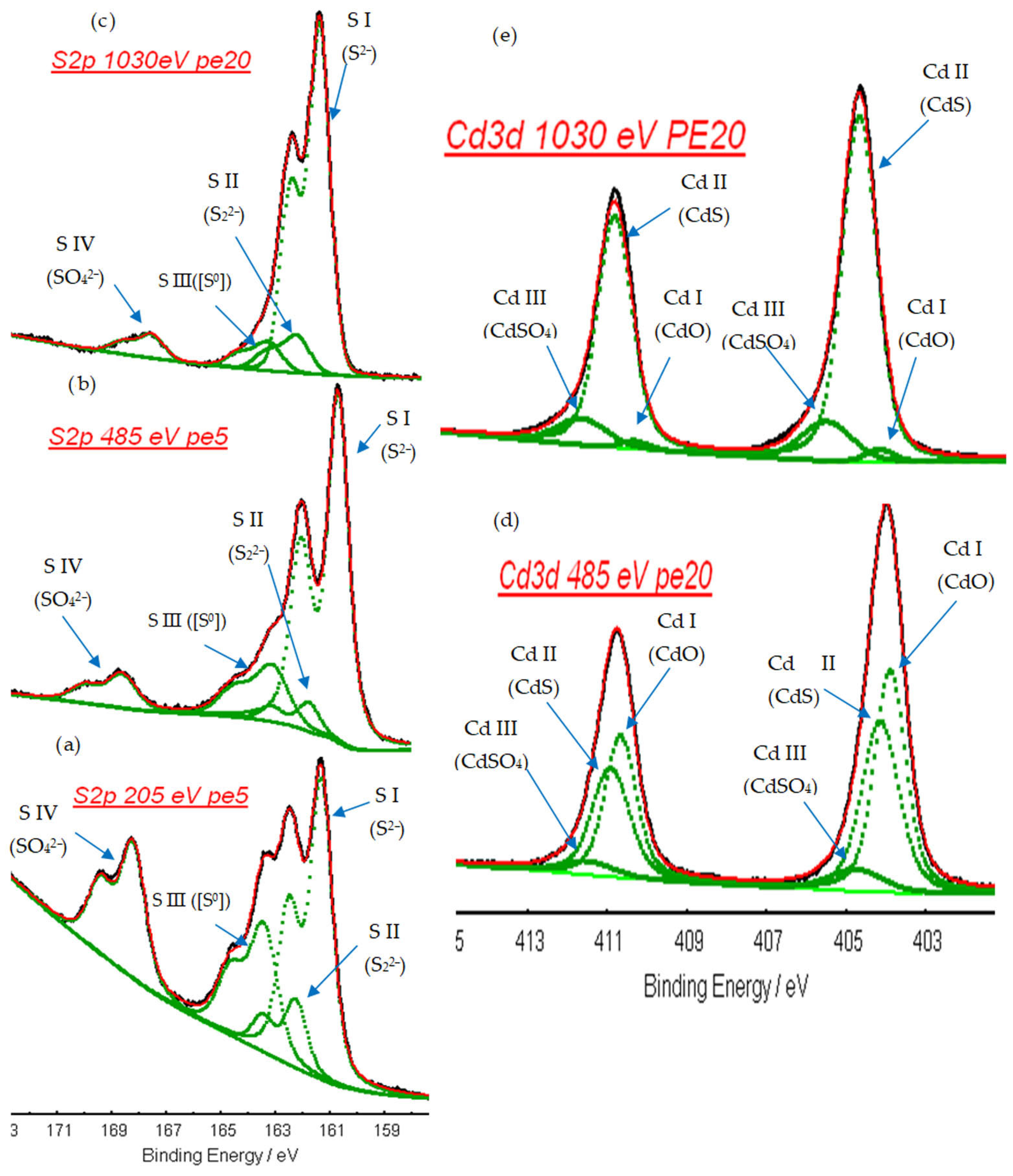
It has been shown that the sulfur spectra contain at least four components: S I, S II (chemical shift relative to S I +0.94 eV), S III (+2.11 eV), and S IV (+6.9 eV), all of them being doublets due to the spin—orbit splitting of the 2p term. The S I component belongs to the initial CdS; the S II component can be assumed to refer to S
22- disulfide ions that may appear on the surface of cadmium sulfide due to its reconstruction and/or oxidation. The S III component (
Figure 7d) is related to elemental sulfur, which is often observed during the oxidation of sulfides of various elements. The S IV component belongs to sulfate ions (SO
42−); the relative intensity of components S II, S III, and S IV, accompanied by an increase in the energy of the exciting radiation (and, therefore, a decrease in the contribution of surface atoms to the recorded signal), decreases. The dependence of the average free travel length of the electrons on the energy of the exciting radiation for Cd 3d and S 2p (data obtained using the TTP-2m,
www.quases.com (accessed on 1 October 2022)) revealed the fact that all of the listed components belong to the surface. The spectra of Cd 3d contain three components: Cd I, Cd II (chemical shift from Cd I +0.37 eV), and Cd III (+1.48 eV) (
Figure 1d,e). It is evident that one of these components, Cd II, corresponds to CdS, and the others can refer to a number of different oxidation products of cadmium in air: Cd I–CdO and/or Cd(OH)
2, or Cd III–CdSO
4. The relative intensity of the components and Cd I decrease along with an increase in the energy of the excitation radiation; therefore, this component belongs to the surface. The approximate thickness of the oxidized nanolayer on the surface of the films is 2–3 monolayers.
The oxidized layer thickness on the surface of the films was estimated approximately based on a regularity: when the thermal treatment duration of the CdS1−xSex films increases, the number of oxidized components in the spectra corresponding to SO42−SeO32− increases.
Consequently, the oxidation products are CdSO4 an CdSeO3, as well as CdCO3 (in an amount of not more than 5–10%). In this case, the CdSiO3 phase is formed on the surface of the polycrystalline CdS1−xSex films applied on a rough sitall substrate (glass ceramics) during their heat treatment in the form of crystallites 1–4 microns in size, located along grain boundaries and film defects.
The oxidized surface of the CdS
1−xSe
x films was studied by XFS method. The CdS powder, exposed to air for a long time, was used as a model sample to study the condition of the film surface. X-ray photoelectron spectra of the powder were recorded using a synchrotron radiation source to accurately determine the spectra parameters (Lorentz component peak width, the chemical shift magnitude between the components, and the number of components, as well as which of them were related to the surface and which referred to the grain volume). The spectrum of the sample in the range of kinetic energies of 100–1040 eV, obtained under an exciting radiation energy of 1030 eV, is shown in
Figure 6.
It is apparent that characteristic photoemission lines of cadmium, sulfur, oxygen, and carbon are present in the spectra.
The spectra of the Cd 3d and S2p regions were recorded under different exciting radiation energies: 1030 and 485 eV (Cd, S) and 205 eV (S). The sulfur spectra (
Figure 7a–c) contain at least four components: S I, S II (chemical shift is relative to S I +0.94 eV), S III (+2.11 eV), and S IV (+6.9 eV). The SI component is related to the initial cadmium sulfide; the nature of the S II component is not completely clear. Based on the literature data, it is assumed to refer to disulfide ions S
22−, which can appear on the surface of cadmium sulfide due to their reconstruction and/or oxidation. The S III component, based on the literature data, belongs to elemental sulfur, which is often observed during the oxidation of sulfides of various elements and is probably formed by the following reaction:
The S IV component refers to sulfate ions (SO
42−), which are formed as a result of the following interaction:
Figure 7a–c shows that the relative intensity of components S II, S III, and S IV decreases along with an increase in the energy of the exciting radiation (and, consequently, a decrease in the contribution of surface atoms to the recorded signal). The dependence of the mean free path of electrons on the energy of exciting radiation for Cd3d and S2p is presented in
Table 2 (data were obtained using the TTP-2m program).
It follows that all the listed components belong to the surface. Since the relative intensity of the S III and S IV components in the spectra is similar, and proportionality is maintained between them when the energy of the exciting radiation changes, the products to which they belong are most likely located in the same surface layer.
The Cd 3d spectra contain three components: Cd I, Cd II (chemical shift relative to Cd I +0.37 eV), and Cd III (+1.48 eV) (
Figure 7d,e).
Obviously, one of these components, Cd II, corresponds to CdS, and the others can be related to a number of different products of oxidizing cadmium in air: Cd I–CdO and/or Cd(OH)
2, or Cd III–CdSO
4.
Figure 7d,e demonstrates that the relative intensity of the components and Cd I decrease when the energy of the exciting radiation increases (and, consequently, the contribution of surface atoms to the recorded signal decreases); therefore, this component belongs to the surface. The ratio of Cd II/Cd III (CdS/CdSO
4) intensities increases when the energy of the exciting radiation increases, which is consistent with a change in the ratio of the intensities of the SI/SIV (S
2−/SO
42−) components.
Hence, the model sample surface of the CdS powder is significantly oxidized. The oxidation products are CdSO4, CdO, and/or Cd(OH)2, as well as elemental sulfur.
Later, the surface of the CdS
1−xSe
x (x = 0; 0.2; 0.8) films, annealed at temperatures of 823–873 K for 5–60 min, was studied using a laboratory X-ray source (MgKα). All the samples of the films were significantly recharged (4–7 eV); therefore, all the below spectra and values of binding energies are given by deducting recharging. The results of determining the position of the lines in the panoramic spectrum of the CdS
0.
8Se
0.
2 film (
Figure 8) are presented in
Table 3. The data obtained in this work are illustrated in
Figure 9.
Figure 9a shows that the carbon on the surface of the films has a different nature. First, carbon from the spectrometer deposited during sample application (the oils are used from diffusion pumps, and organic compounds are obtained from the environment) is 285 eV and 286.5 eV (taking into account charging). Second, the peak corresponding to cadmium carbonate is 288.9 eV (considering charging), the relative content of which does not exceed 3–5%.
The O 1s spectrum (
Figure 9b) is quite wide due to the superposition of a number of peaks corresponding to oxygen-containing ions (SO
42−; SeO
32−; CO
32−; OH
−, etc.), for which the position of the oxygen lines is approximately the same. In the O1s spectrum, there is no peak corresponding to the Cd-O bond (529–530 eV). This is probably a companion of the O 1s peak.
At least two components with a small chemical shift relative to each other are present in the Cd3d spectra (
Figure 9c). However, in this case, the metal spectra are not informative, since the positions of the Cd3d
5/2 lines for various possible oxidation products, containing Cd
2+(CdSO
4, CdSeO
3, CdCO
3, CdS, CdSe, etc.), differ slightly (by less than 1 eV). Therefore, in this work, conclusions about the oxidation products of the surface of the CdS
1−xSe
x films were mainly made based on the spectra of other elements (S, Se, etc.).
Two components were identified in the S2p spectra whose chemical shifts (6.8–7.2 eV towards high binding energies) are consistent with the values typical of sulfide and cadmium sulfate (
Figure 9d and
Table 3). The more intense one corresponds to S
2−, and the less intense one is related to SO
42−. The relative fraction of the oxidized component increases along with the increase in temperature and duration of annealing of films.
Figure 7 demonstrates that weak peaks of Cd3d
5/2 (binding energy of about 173–174 eV) are superimposed on the S2p spectrum that arise due to the design peculiarities of the anode Al Kα (the presence of an aluminum anode in close proximity to a magnesium one).
In the Se3d spectra, two components were successively identified, the chemical shift value between which corresponds to the values typical of selenide (more intense) and cadmium selenite (less intense) (
Figure 9e and
Table 3).
In addition, Cl
− is present in the films, which is part of cadmium chloride used as a flux (
Figure 9f). Obviously, the removal of the flux from the surface of the samples after annealing does not occur completely, while part of the cadmium chloride remains on the surface.
The energy-dispersive X-ray spectroscopy (EDX) of the films annealed with different air oxygen accesses showed that the composition of the films in terms of area was uniform enough. In addition to the main elements of the paste (Cd, S, and Se), the films contain a significant amount of oxygen, the concentration of which in the finished films increases in proportion to the increase in the oxygen concentration in the furnace reactor during heat treatment. The heat treatment of the films by method 2 is shown to reduce the oxygen content in them by 40–50%.
The S/Se data on the surface obtained by the XPS method are well consistent with the results of XRD and X-ray diffraction, which indicates the absence of surface segregation. Since cadmium sulfide has a greater vapor elasticity than selenide does, during the preliminary synthesis of the solid solution and the subsequent heat treatment of the films, it is lost slightly more, leading to a change in the composition of the solid solution. Within the accuracy of ±1–2%, the composition of the films coincides with the initial composition of the pastes.
When activating the photosensitivity of the film, a nanolayer of dielectric phase (CdSO4 and/or CdSeO3) is formed on the surface of each crystallite, leading to the formation of a dielectric–semiconductor transition. The composition and thickness of this layer and the content of foreign impurities (CdCl2, CdSiO3, and CdCO3) determine the electrophysical properties of polycrystalline films. The parameters of this layer can be shown to be controlled by optimizing the temperature range of the treatment, as well as the composition of the applied pastes. This study revealed that the oxidation of the CdS and CdSe powders is a complex heterogeneous process that involves intermediate steps. It is impossible to unambiguously say which of the reactions, oxidation to sulfate (selenite) or their decomposition to CdO, occurs when interacting with oxygen. Depending on the temperature and composition of the gas phase in which the oxidation occurs, one group of reactions will be suppressed, and the other will be most developed, which will affect the final phase composition of the oxidation products.
The grain size of the films can be controlled by temperature and the heat treatment duration. It was found that the average crystallite size in the film linearly depends on the annealing time (
Figure 10).
Consequently, the grain growth rate is limited by the processes occurring on the surface and is independent of the composition x.


 ,
, 


